a new cmos current-mode folding amplifier · posed circuit was confirmed using tanner ... of a...
TRANSCRIPT

892 M. A. AL-ABSI, S. A. MAHEMOOD, M. T. ABUELMA’ATTI, A NEW CMOS CURRENT-MODE FOLDING AMPLIFIER
A New CMOS Current-Mode Folding Amplifier
Munir A. AL-ABSI, Shaker A. MAHEMOOD, Muhammad T. ABUELMA’ATTI
Electrical Engineering Department, King Fahd University of Petroleum & Minerals, Dhahran, Saudi Arabia
Abstract. In this paper, a new CMOS current-mode folding amplifier is proposed. The circuit is designed using MOSFETs operating in strong inversion. The design produces a nearly ideal saw-tooth input-output charac-teristic which is a mandatory requirement in folding analog-to-digital converters. The functionality of the pro-posed circuit was confirmed using Tanner simulation tools in 0.35 μm CMOS technology. Simulation results are in excellent agreement with the theory.
Keywords Current-mode, saw-tooth generator, folding amplifier, Flash analog-to-digital converter.
1. Introduction The analog-to-digital converter (ADC) is one of the
most important building blocks to interface analog world to digital world. ADCs applications are widely used in numerous applications including digital telephone transmission, cell phones, medical imaging and wireless nodes.
ADCs are found in different architectures and each one has a unique set of characteristics and different limitations. Consequently, the most convenient analog-to-digital conversion technique should be chosen based on the application. The most common types of ADCs are flash, successive approximation and sigma-delta. The fastest and conceptually simplest conversion process is the full flash or parallel flash ADC [1], [2]. However, for N-bit resolution, it needs a 2N – 1 comparators, and 2N resistors to generate reference voltages, which leads to higher power con-sumption and larger silicon area.
Folding ADC is used to reduce the complexity of flash ADC while maintaining a relatively good conversion speed. For example, for (N = m + l) bits resolution, with m most significant bits and l least significant bits, the number of comparators required for folding ADC is 2m
– 1 comparators (for MSB) and 2l – 1 comparators (for LSB). The total number of comparators used is (2m – 1) + (2l – 1) which can be as low as less than half of the number of comparators used in flash ADC which is 2N – 1.
On the other hand, the applications of CMOS current-mode circuits have increased dramatically. Current-mode
circuits have some recognized advantages over voltage-mode counterparts. The current-mode circuits are more suitable for low voltage design compared to voltage mode circuits.
A key element in the design of the folding ADC is the folding amplifier having a saw-tooth input-output characteristic. A conventional voltage-mode folding ampli-fier is built around a differential pair [3], [4]. It is well known, however, that the differential pair is not suitable for low voltage design because of nonlinearity problems [5]. Moreover, the input-output characteristic of a differential amplifier-based folding amplifier is sine-wave shaped. This would result in digitization error. A current-mode folding amplifier based on current mirror was proposed in [6]. In reference [7], the authors presented a current-mode folding amplifier controlled by coarse ADCs for the design of a current-mode folding ADC. The input-output charac-teristic of the amplifiers proposed in [6], [7] is a triangular-wave which will degrade the conversion accuracy. Recently, some pure linear analog preprocessing voltage-mode folding circuits have been presented to generate saw-tooth input-output characteristic [8], [9].However, in the open literature, there are no current-mode folding circuits that generate saw-tooth input-output characteristic.
In this paper, a new CMOS current-mode folding amplifier that generates a saw-tooth input-output characteristic is presented. The paper is organized as follows. Section 2 presents a brief description of the folding concept. The proposed design is presented in Section 3. Simulation results are presented in Section 4. Mismatch analysis study is described in Section 5. The paper conclusion is presented in Section 6.
2. Folding ADC Folding is a type of analog preprocessing that is used
to produce more than one zero-crossing point. Folding is used to reduce the number of comparators, and thus, the power consumption and the silicon area of a flash ADC. The block diagram of a current-mode folding ADC is shown in Fig 1. The input signal is applied to an analog preprocessing circuit called folding amplifier, and the output of this folding circuit is connected to a fine quantizer. Also, the input signal is directly connected to a coarse quantizer. The coarse digital output represents the most significant bits (MSB) and the fine digital output will produce the least significant bits (LSB).

RADIOENGINEERING, VOL. 22, NO. 3, SEPTEMBER 2013 893
Fig. 1. Block diagram of current-mode folding flash ADC.
The output of the folding amplifier could be saw-tooth, triangular or sinusoidal-shaped based on the architecture. Folding the input to a triangular or sinusoidal-shaped output will lead to errors in the digitized output and compensation would be required. As an example a 5-bits folding ADC and errors produced from triangular-shaped output folding amplifier is shown in Fig 2. It is clear from Fig. 2 that the digital output, 01010, is the same for the two different analog inputs, 0.36IFS and 0.46IFS. Thus, one digital output represents two analog inputs.
001
010
011
100
101
110
111
Iin = 0.36IFS
(01010)Iin = 0.46IFS
( 01010 )
000 IinxIFS
0 1/4 1/2 3/4 1
010 010
01
01
00
01
10
11
Iin
xIFS
1/4 1/2 3/4 0 1
Fine
Bits
Coar
seBi
ts
Fig. 2. 5-bit folding ADC using triangular-shaped folding
amplifier.
It is well known that saw-tooth input-output charac-teristic is the best that will eliminate, or minimize, the digitization error as depicted in Fig. 3. Here it is clear that only one digital output represents one analog input.
3. Proposed Current-Mode Folding Amplifier A current-mode folding amplifier has been developed
to generate saw-tooth-shaped input-output characteristic. Fig. 4 shows the concept used to develop the proposed folding amplifier. It consists of two blocks each block produces the shape of the signal shown in Fig. 4 and the two signals are summed together to produce the required saw-tooth input-output characteristic.
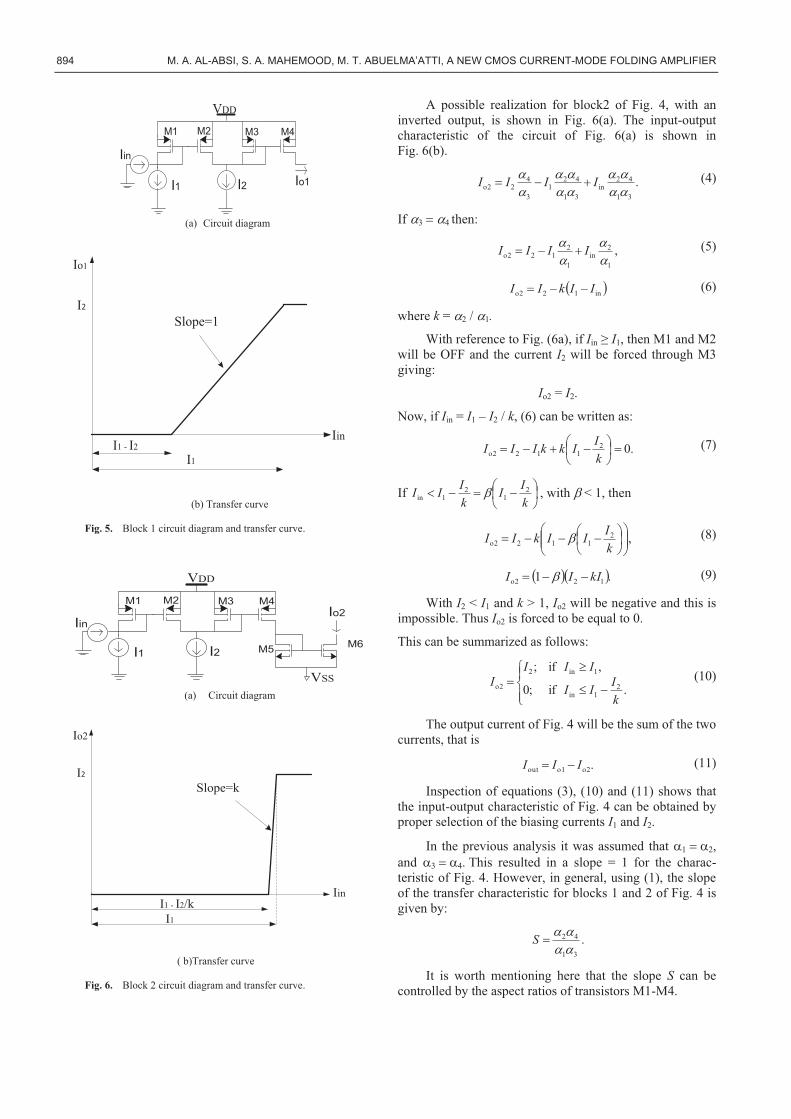
A possible realization for block1 of Fig. 4 is shown in Fig. 5(a). It consists of two current mirrors connected in
11
01
00
01
10
11
Iin
xIFS
1/4 1/2 3/4 0 1
011
101
000
001
010
011
100
101
110
111
Iin
xIFS
0 1/4 1/2 3/4 1
Iin = 0.36IFS
(01011)Iin = 0.92IFS
( 11101)
FineB
itsCo
arseB
its
Fig. 3. 5-bit folding ADC using saw-tooth-shaped of folding
amplifier.
Block 1
Block 2
+
IinI1
IoutI2
Io1
Iin
I1
I2
I1 - I2
Slope=1
Io2
Iin
I2
I1 - I2/kI1
Slope=k
Fig. 4. The concept used in developing the proposed folding amplifier.
cascade. The circuit is designed so that for small input current, the output is zero, while for large input current the output current is constant and equal to �I2 where I2 is the bias current and � is the aspect ratio of transistors M1 and M2. The output current as a function of the input current for the block1 is shown in Fig. 5(b).
With reference to Fig. 5(a), the output current is given by:
31
42in
31
421
3
42o1 ��
������
�� IIII ��� (1)
where ai = Wi / Li is the aspect ratio of transistor Mi.
If �������, and ������then:
.in12o1 IIII ��� (2)
With reference to Fig. 5a, if Iin > I1, then M1 and M2 will be OFF, current I2 will be forced to go through M3 giving Io1 = I2. If Iin < I1 – I2 then the output current will be forced to be negative, which is impossible. Thus, Io1 will be equal to zero. This is summarized in (3).
��
���
�. if0
, if
21in
1in2o1 III
IIII (3)
MSB
LSB
Coarse Flash ADC
Fine Flash ADC Folding
Amplifier
894 M. A. AL-ABSI, S. A. MAHEMOOD, M. T. ABUELMA’ATTI, A NEW CMOS CURRENT-MODE FOLDING AMPLIFIER
VDD
Iin
M1 M3M2 M4
I2I1 Io1
(a) Circuit diagram
Iin
I1
I2
I1 - I2
Io1
Slope=1
(b) Transfer curve
Fig. 5. Block 1 circuit diagram and transfer curve.
M6
Iin
M1 M3M2 M4
I2I1
Io2
M5
VDD
VSS (a) Circuit diagram
Io2
Iin
I1
I2
I1 - I2/k
Slope=k
( b)Transfer curve
Fig. 6. Block 2 circuit diagram and transfer curve.
A possible realization for block2 of Fig. 4, with an inverted output, is shown in Fig. 6(a). The input-output characteristic of the circuit of Fig. 6(a) is shown in Fig. 6(b).
.31
42in
31
421
3
42o2 ��
������
�� IIII ��� (4)
If ������then:
,1
2in
1
212o2 �
��� IIII ��� (5)
� �in12o2 IIkII ��� (6)
where k = �2 / �1.
With reference to Fig. (6a), if Iin ≥ I1, then M1 and M2 will be OFF and the current I2 will be forced through M3 giving:
Io2 = I2.
Now, if Iin = I1 – I2 / k, (6) can be written as:
.02112o2 ��
��
��� ����
kIIkkIII (7)
If ���
��� ����
kII
kIII 2
12
1in � , with � < 1, then
,2112o2 ��
�
����
����
��� ����
kIIIkII � (8)
� �� �.1 12o2 kIII ��� � (9)
With I2 < I1 and k > 1, Io2 will be negative and this is impossible. Thus Io2 is forced to be equal to 0.
This can be summarized as follows:
��
��
��
�� . if;0
, if;2
1in
1in2
o2
kIII
IIII (10)
The output current of Fig. 4 will be the sum of the two currents, that is
.o2o1out III �� (11)
Inspection of equations (3), (10) and (11) shows that the input-output characteristic of Fig. 4 can be obtained by proper selection of the biasing currents I1 and I2.
In the previous analysis it was assumed that �������, and �������This resulted in a slope = 1 for the charac-teristic of Fig. 4. However, in general, using (1), the slope of the transfer characteristic for blocks 1 and 2 of Fig. 4 is given by:
.31
42
����
�S
It is worth mentioning here that the slope S can be controlled by the aspect ratios of transistors M1-M4.

RADIOENGINEERING, VOL. 22, NO. 3, SEPTEMBER 2013 895
The complete circuit diagram of the proposed current mode folding amplifier with a folding factor of 4 is shown in Fig. 7 with all MOSFETs substrates connected to the respected sources.
Current Copier
Rload
Mn8
M1 M3M2 M4
I2I1
M5 M7M6 M8
I4I3
M9 M11M10 M12
I6I5
M13 M15M14 M16
I8I7
M29 M31M30 M32
I88I77 Mn7
M25 M27M26 M28
I66I55 Mn5 Mn6
M21 M23M22 M24
I44I33 Mn3 Mn4
M17 M19M18 M20
I22I11 Mn1 Mn2
VDD
VDD
VDD
VDD
VDD
VDD
VDD
VDD
VSS
VSS
VSS
VSS
Mp1 Mp2
VDD
Iin
VSS
Mp3 Mp4
VSS
VDD
VDD
Mp5 Mp6
VSSVDD
Mp7 Mp8
VSS
VDD
Mp9 Mp10
VSS
VDD
Mp11 Mp12
VSS
VDD
Mp13 Mp14
VSS
VSS
Mi1
VDD
Mp15 Mp16
VSS
Mi2
Mi3
Mi4
Mi5
Mi6
Mi7
Mi8
Mi9
Fig. 7. Current-mode folding amplifier with a folding factor of 4.
4. Simulation Results and Discussion The proposed circuit of Fig. 7 was simulated using
Tanner simulation tools in 0.35 μm CMOS process technology with DC supply voltage VDD = − VSS = 1 V and bias currents as follows;
I1 = I11 = 9 �A,
I2 = I22 = I4 = I44 = I6 = I66 = I8 = I88 = 9 �A,
I7 = I77 = 4I1,
I5 = I55 = 3I1,
and I3 = I33 = 2I1.
The output current was measured by forcing it through a grounded resistive load of 1 k�. All transistors aspect ratios are given in Tab. 1.
Transistor Aspect ratio
M1,M2,M5,M6 M9,M10,M13,M14 M17,M21,M25,M29
2 μm /2 μm
M3,M4,M7,M8M11,M12,M15,M16,M19,M20,M23,M24M27,M28,M31,M32
4 μm/ 2μm
M18,M22,M26,M30 50 μm/2 μm Mi1-Mi9 &Mp1-Mp16 20 μm/4 μm
Mn1,Mn2,Mn3,Mn4Mn5,Mn6,Mn7,Mn8 2.4 μm/2 μm
Tab. 1. Transistors aspect ratios.
4.1 DC Simulation Results The DC simulation results of the proposed folding
amplifier are shown in Fig. 8. It appears from Fig. 8 that the simulated result is a saw-tooth-shape which confirms the functionality of the developed design.
Fig. 8. Input and output characteristics of current-mode
amplifier.
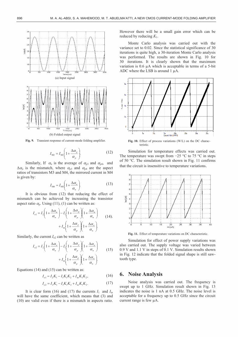
4.2 Transient Simulation Results The proposed circuit was simulated for transient
analysis. The input is a sine wave signal as shown in Fig. 9(a). It is evident from Fig. 9(b) that simulation result confirms the functionality of the circuit.
5. Mismatch Analysis Since the design is based on current mirrors, the
accuracy of the folding amplifier will be affected by the mirror performance. Consequently, it is important to study the effect of mismatch in device dimension that may result during fabrication process [10]. With reference to the core circuits in Fig. 5(a) and Fig. 6(a) assuming a mismatch in the threshold voltages between M1 and M2 such that �p is the average of �p1 and �p2, and ��p is the mismatch, where �p1 and �p2 are the aspect ratios of transistors M1 and M2 forming the mirror respectively and assuming all other parameters are matched, the mirrored current in M2 is given by:
896 M. A. AL-ABSI, S. A. MAHEMOOD, M. T. ABUELMA’ATTI, A NEW CMOS CURRENT-MODE FOLDING AMPLIFIER
(a) Input signal
(b) Folded output signal
Fig. 9. Transient response of current-mode folding amplifier.
.1M2M2 ���
����
� ���
p
pII�� (12)
Similarly, If ��n is the average of �p3 and �p4, and ��n is the mismatch, where �p3 and �p4 are the aspect ratios of transistors M3 and M4, the mirrored current in M4 is given by:
.1M3M4 ���
����
� ���
n
nII�� (13)
It is obvious from (12) that reducing the effect of mismatch can be achieved by increasing the transistor aspect ratio �p. Using (11), (1) can be written as:
.11
111
in
12o1
���
����
� ���
��
����
� ���
���
����
� ���
��
����
� �����
�
����
� ���
n
n
p
p
n
n
p
p
n
n
I
III
��
��
��
��
��
(14).
Similarly, the current Io2 can be written as
.11
111
in
12o2
���
����
� ���
��
����
� ���
���
����
� ���
��
����
� �����
�
����
� ���
n
n
p
p
n
n
p
p
n
n
I
III
��
��
��
��
��
(15)
Equations (14) and (15) can be written as: ,21in21112o1 KKIKKIKII ��� (16)
.21in21112o2 KKIKKIKII ��� (17)
It is clear form (16) and (17) the currents I1 and Iin will have the same coefficient, which means that (3) and (10) are valid even if there is a mismatch in aspects ratio.
However there will be a small gain error which can be reduced by reducing K1.
Monte Carlo analysis was carried out with the variance set to 0.02. Since the statistical significance of 30 iterations is quite high, a 30-iteration Monte Carlo analysis was performed. The results are shown in Fig. 10 for 30 iterations. It is clearly shown that the maximum variation is 0.6 μA which is acceptable in terms of a 5-bit ADC where the LSB is around 1 μA.
Fig. 10. Effect of process variations (W/L) on the DC charac-
teristic.
Simulation for temperature effects was carried out. The temperature was swept from −25 °C to 75 °C in steps of 50 °C. The simulation result shown in Fig. 11 confirms that the circuit is insensitive to temperature variations.
Fig. 11. Effect of temperature variations on DC characteristic.
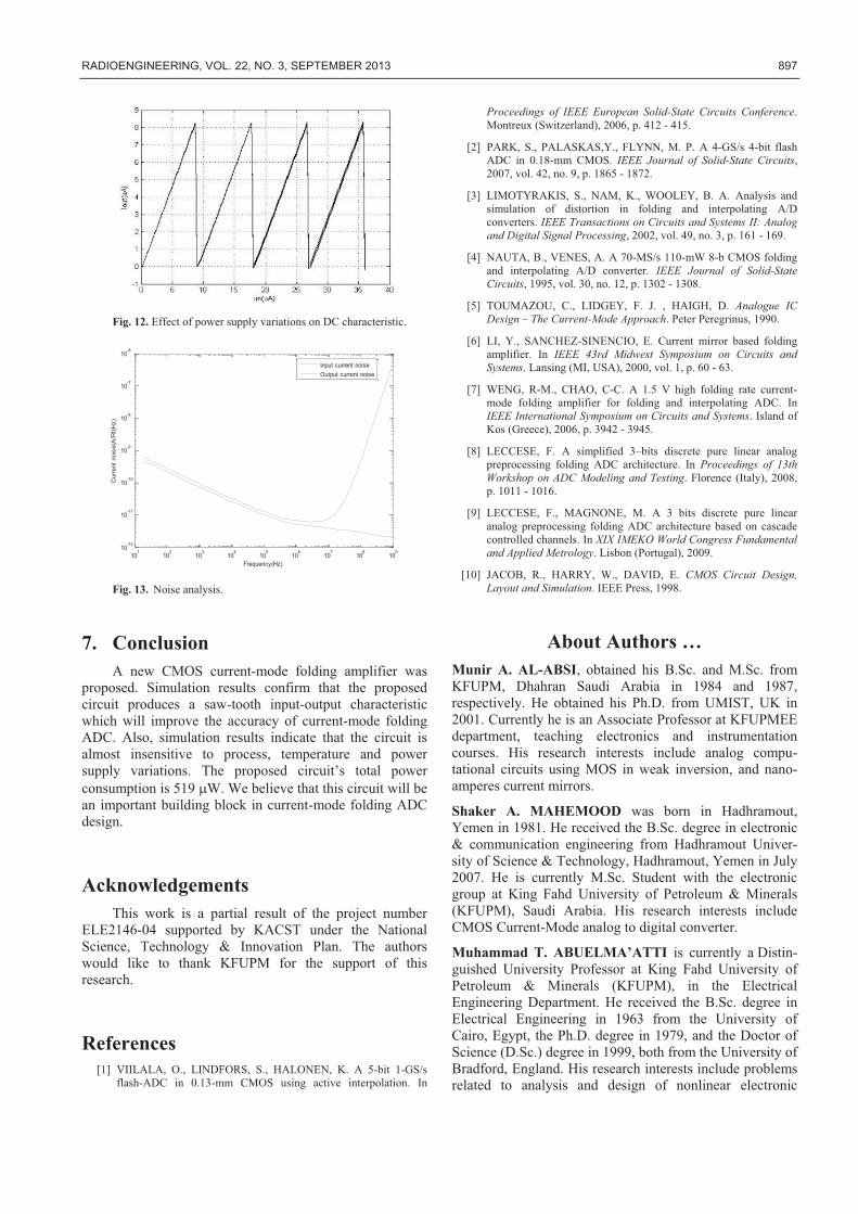
Simulation for effect of power supply variations was also carried out. The supply voltage was varied between 0.9 V and 1.1 V in steps of 0.1 V. Simulation results shown in Fig. 12 indicate that the folded signal shape is still saw-tooth type.
6. Noise Analysis Noise analysis was carried out. The frequency is
swept up to 1 GHz. Simulation result shown in Fig. 13 indicates the noise is 1 nA at 0.5 GHz. The noise level is acceptable for a frequency up to 0.5 GHz since the circuit current range is few μA.
RADIOENGINEERING, VOL. 22, NO. 3, SEPTEMBER 2013 897
Fig. 12. Effect of power supply variations on DC characteristic.
Fig. 13. Noise analysis.
7. Conclusion A new CMOS current-mode folding amplifier was
proposed. Simulation results confirm that the proposed circuit produces a saw-tooth input-output characteristic which will improve the accuracy of current-mode folding ADC. Also, simulation results indicate that the circuit is almost insensitive to process, temperature and power supply variations. The proposed circuit’s total power consumption is 519 �W. We believe that this circuit will be an important building block in current-mode folding ADC design.
Acknowledgements This work is a partial result of the project number
ELE2146-04 supported by KACST under the National Science, Technology & Innovation Plan. The authors would like to thank KFUPM for the support of this research.
References [1] VIILALA, O., LINDFORS, S., HALONEN, K. A 5-bit 1-GS/s
flash-ADC in 0.13-mm CMOS using active interpolation. In
Proceedings of IEEE European Solid-State Circuits Conference. Montreux (Switzerland), 2006, p. 412 - 415.
[2] PARK, S., PALASKAS,Y., FLYNN, M. P. A 4-GS/s 4-bit flash ADC in 0.18-mm CMOS. IEEE Journal of Solid-State Circuits, 2007, vol. 42, no. 9, p. 1865 - 1872.
[3] LIMOTYRAKIS, S., NAM, K., WOOLEY, B. A. Analysis and simulation of distortion in folding and interpolating A/D converters. IEEE Transactions on Circuits and Systems II: Analog and Digital Signal Processing, 2002, vol. 49, no. 3, p. 161 - 169.
[4] NAUTA, B., VENES, A. A 70-MS/s 110-mW 8-b CMOS folding and interpolating A/D converter. IEEE Journal of Solid-State Circuits, 1995, vol. 30, no. 12, p. 1302 - 1308.
[5] TOUMAZOU, C., LIDGEY, F. J. , HAIGH, D. Analogue IC Design – The Current-Mode Approach. Peter Peregrinus, 1990.
[6] LI, Y., SANCHEZ-SINENCIO, E. Current mirror based folding amplifier. In IEEE 43rd Midwest Symposium on Circuits and Systems. Lansing (MI, USA), 2000, vol. 1, p. 60 - 63.
[7] WENG, R-M., CHAO, C-C. A 1.5 V high folding rate current-mode folding amplifier for folding and interpolating ADC. In IEEE International Symposium on Circuits and Systems. Island of Kos (Greece), 2006, p. 3942 - 3945.
[8] LECCESE, F. A simplified 3–bits discrete pure linear analog preprocessing folding ADC architecture. In Proceedings of 13th Workshop on ADC Modeling and Testing. Florence (Italy), 2008, p. 1011 - 1016.
[9] LECCESE, F., MAGNONE, M. A 3 bits discrete pure linear analog preprocessing folding ADC architecture based on cascade controlled channels. In XIX IMEKO World Congress Fundamental and Applied Metrology. Lisbon (Portugal), 2009.
[10] JACOB, R., HARRY, W., DAVID, E. CMOS Circuit Design, Layout and Simulation. IEEE Press, 1998.
About Authors … Munir A. AL-ABSI, obtained his B.Sc. and M.Sc. from KFUPM, Dhahran Saudi Arabia in 1984 and 1987, respectively. He obtained his Ph.D. from UMIST, UK in 2001. Currently he is an Associate Professor at KFUPMEE department, teaching electronics and instrumentation courses. His research interests include analog compu-tational circuits using MOS in weak inversion, and nano-amperes current mirrors.
Shaker A. MAHEMOOD was born in Hadhramout, Yemen in 1981. He received the B.Sc. degree in electronic & communication engineering from Hadhramout Univer-sity of Science & Technology, Hadhramout, Yemen in July 2007. He is currently M.Sc. Student with the electronic group at King Fahd University of Petroleum & Minerals (KFUPM), Saudi Arabia. His research interests include CMOS Current-Mode analog to digital converter.
Muhammad T. ABUELMA’ATTI is currently a Distin-guished University Professor at King Fahd University of Petroleum & Minerals (KFUPM), in the Electrical Engineering Department. He received the B.Sc. degree in Electrical Engineering in 1963 from the University of Cairo, Egypt, the Ph.D. degree in 1979, and the Doctor of Science (D.Sc.) degree in 1999, both from the University of Bradford, England. His research interests include problems related to analysis and design of nonlinear electronic
101
102
103
104
105
106
107
108
109
10-12
10-11
10-10
10-9
10-8
10-7
10-6
Frequency(Hz)
Cur
rent
noi
se(A
/Rt(H
z)
Input current noiseOutput current noise

898 M. A. AL-ABSI, S. A. MAHEMOOD, M. T. ABUELMA’ATTI, A NEW CMOS CURRENT-MODE FOLDING AMPLIFIER
circuits and systems, analog integrated circuits and active networks design. He is the author or co-author of over 600 journal articles and technical presentations. He was the recipient of the excellence in teaching award in 1995, the
excellence in research award in 1996, 2001 and 2006 (with distinction), and the Distinguished University Professor award in 2008 and 2011, all from King Fahd University of Petroleum & Minerals, Dhahran Saudi Arabia.