a low power cmos analog circuit design for acquiring multichannel eeg signals
TRANSCRIPT
International Journal of VLSI design & Communication Systems (VLSICS) Vol.6, No.1, February 2015
DOI : 10.5121/vlsic.2015.6103 25
A LOW POWER CMOS ANALOG CIRCUIT
DESIGN FOR ACQUIRING MULTICHANNEL
EEG SIGNALS
G. Deepika1 and Dr. K.S.Rao
2
1Department of Electronics and Communication Engineering,
RRS College of Engineering & Technology, Hyderabad, India 2Department of Electronics and Communication Engineering,
ANURAG Group of Institutions, Hyderabad, India
ABSTRACT
EEG signals are the signatures of neural activities and are captured by multiple-electrodes and the signals
are recorded from pairs of electrodes. To acquire these multichannel signals a low power CMOS circuit
was designed and implemented. The design operates in weak inversion region employing sub threshold
source coupled logic. A 16 channel differential multiplexer is designed by utilizing a transmission gate with
dynamic threshold logic and a 4 to 16 decoder is used to select the individual channels. The ON and OFF
resistance of the transmission gate obtained is 27 ohms and 10 M ohms respectively. The power dissipation
achieved is around 337nW for a dynamic range of 1µV to 0.4 V.
KEYWORDS
EEG, Subthreshold , Differential MUX, Low Power
1. INTRODUCTION
The billions of neurons present in the cerebral cortex and any number of them may be active at a
particular moment of time produces brains electrical activity as seen the scalp EEG, which is a
continuum of electrical discharges that may vary from moment to moment. This electrical
activity is different in frequency and amplitude over different areas of brain. To obtain a complete
and valid picture of the brains electrical activity, it is necessary to simultaneously record samples
of activity from different areas of the scalp.
The sophistication of EEG recording systems has closely followed technological developments in
electronics. In late 1940’s when the technology was limited EEG recordings were made on
machines having only two or four channels which limited the simultaneous recording of samples
from pairs of electrodes, and such recording is inadequate for describing the function of entire
brain. This placed the demand for multichannel machines that can record the samples from pairs
of electrodes placed over the entire scalp simultaneously.
International Journal of VLSI design & Communication Systems (VLSICS) Vol.6, No.1, February 2015
26
The placement of electrodes in this system depends upon the measurements made from standard
land marks on the skull. In general, the EEG signals are the projection of neural activities that are
attenuated by the scalp. However, on the scalp the amplitudes commonly lie within 10–100 µV.
The International Federation of Societies for Electroencephalography and Clinical
Neurophysiology has recommended the conventional electrode setting (also called 10–20) for 21
electrodes (excluding the earlobe electrodes) [17]. The recordings of EEG from various pairs of
electrodes can be made as mentioned in the Table 1.
Table -1: Electrode combination for recording EEG
S.NO Longitudinal
Bipolar
Transverse
Bipolar
Referential
Earlobes
1 Fp1 - F7 F7 - Fp1 F7- A1
2 F7 - T3 Fp2 - F8 T3 - A1
3 T3 - T5 F7 - F3 T5 - A1
4 T5 - O1 F3 - Fz F8 - A2
5 Fp2 - F8 Fz - F4 T4 - A2
6 F8 - T4 F4 - F8 T6 - A2
7 T4 - T6 T3 - C3 Fp1 - A1
8 T6 - O2 C3 - Cz F3 - A1
9 Fp1 - F3 Cz - C4 C3 - A1
10 F3 - C3 C4 - T4 P3 - A1
11 C3 - P3 T5 - P3 O1 - A1
12 P3 - O1 P3 - Pz Fp2 - A2
13 Fp2 - F4 Pz - P4 F4 - A2
14 F4 - C4 P4 - T6 C4 - A2
15 C4 - P4 T5 - O1 P4 - A2
16 P4 - O2 O2 - T6 O2 - A2
In Real time system design the major important task is the implementation of high performance
signal processing and conditioning block. Many signal processing applications like from
switching of weak signals to complex processing of audio and video signals requires an essential
component and one such is Analog switch. The building blocks designed with these switches
implemented in CMOS technology proved superior to its counter parts. Implementation of these
blocks depends upon process variations and mismatching of various components and devices[1].
For low power applications, designing of these switches with reduced channel lengths creates
new challenges. The recent advances through new techniques and technologies, provides several
alternatives in implementation.
Several applications in integrated circuit design such as multiplexing, modulation etc, requires a
switch used as a transmission gate. Many modern applications in several areas like mobile
systems [1],[2] sensor networks [3],[4] and implantable biomedical applications[5]. In present
day electronics the necessity for low power has created a major shift in which power dissipation
became an important consideration in performance and area.
International Journal of VLSI design & Communication Systems (VLSICS) Vol.6, No.1, February 2015
This work proposes a new technique utilizing source coupled logic (SCL) circuit biased in sub
threshold region for implementing analog switch achieving low power consumption. The
and threshold voltages of the device will not influence the speed of operation.
In this work sub threshold (STSCL) gates were implemented where the bias current of each cell
can be set as low as 10pA. A brief introduction of SCL circuits, the prop
implementing the low power analog switch ( Transmission Gate) using sub STSCL gates, power
consumption and experimental results are described in the following sections.
2. SUBTHRESHOLD SOURCE
In STSCL circuits the logic operation mainly takes place in current domain and hence the speed
of operation is high. The tail current I
switch will steered to one of the output that depends on the input logic. This c
converted to output voltage by the load resistor R
voltage swing should be adequately high in order to switch the input differential pair (R
The input pair drain source over drive voltage sh
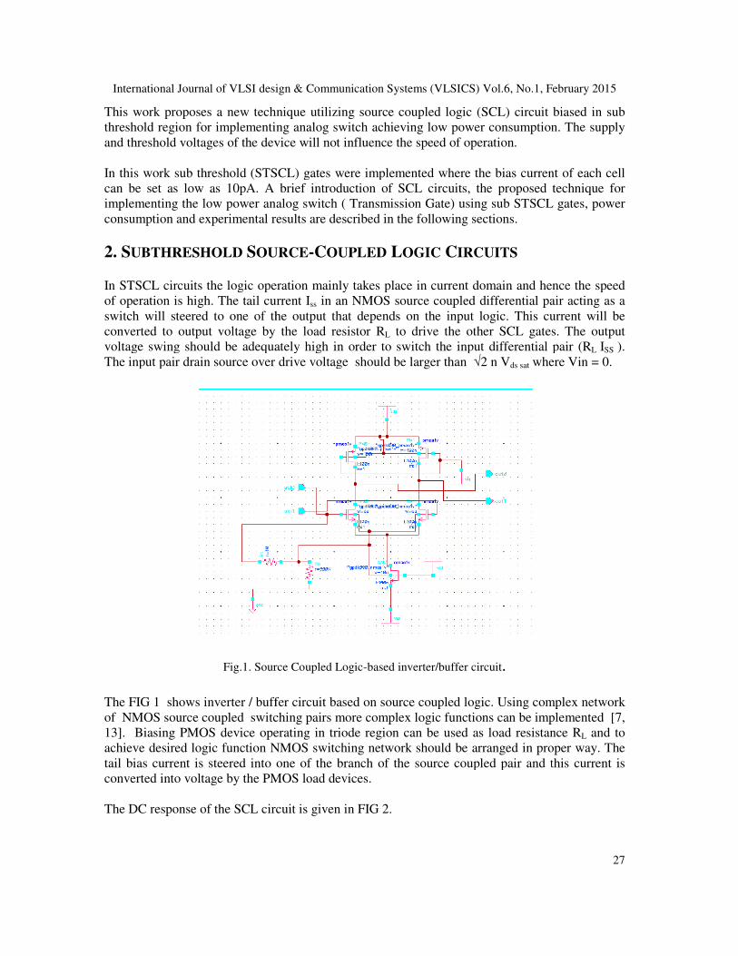
Fig.1. Source Coupled Logic
The FIG 1 shows inverter / buffer circuit based on source coupled logic. Using complex network
of NMOS source coupled switching pairs more
13]. Biasing PMOS device operating in triode region can be used as load resistance R
achieve desired logic function NMOS switching network should be arranged in proper way. The
tail bias current is steered into one of the branch of the source coupled pair and this current is
converted into voltage by the PMOS load devices.
The DC response of the SCL circuit is given in FIG 2.
International Journal of VLSI design & Communication Systems (VLSICS) Vol.6, No.1, February 2015
This work proposes a new technique utilizing source coupled logic (SCL) circuit biased in sub
threshold region for implementing analog switch achieving low power consumption. The
and threshold voltages of the device will not influence the speed of operation.
In this work sub threshold (STSCL) gates were implemented where the bias current of each cell
can be set as low as 10pA. A brief introduction of SCL circuits, the proposed technique for
implementing the low power analog switch ( Transmission Gate) using sub STSCL gates, power
consumption and experimental results are described in the following sections.
OURCE-COUPLED LOGIC CIRCUITS
the logic operation mainly takes place in current domain and hence the speed
of operation is high. The tail current Iss in an NMOS source coupled differential pair acting as a
switch will steered to one of the output that depends on the input logic. This current will be
converted to output voltage by the load resistor RL to drive the other SCL gates. The output
voltage swing should be adequately high in order to switch the input differential pair (R
The input pair drain source over drive voltage should be larger than √2 n Vds sat where Vin = 0.
Fig.1. Source Coupled Logic-based inverter/buffer circuit.
The FIG 1 shows inverter / buffer circuit based on source coupled logic. Using complex network
of NMOS source coupled switching pairs more complex logic functions can be implemented [7,
13]. Biasing PMOS device operating in triode region can be used as load resistance R
achieve desired logic function NMOS switching network should be arranged in proper way. The
teered into one of the branch of the source coupled pair and this current is
converted into voltage by the PMOS load devices.
The DC response of the SCL circuit is given in FIG 2.
International Journal of VLSI design & Communication Systems (VLSICS) Vol.6, No.1, February 2015
27
This work proposes a new technique utilizing source coupled logic (SCL) circuit biased in sub
threshold region for implementing analog switch achieving low power consumption. The supply
In this work sub threshold (STSCL) gates were implemented where the bias current of each cell
osed technique for
implementing the low power analog switch ( Transmission Gate) using sub STSCL gates, power
the logic operation mainly takes place in current domain and hence the speed
in an NMOS source coupled differential pair acting as a
urrent will be
to drive the other SCL gates. The output
voltage swing should be adequately high in order to switch the input differential pair (RL ISS ).
where Vin = 0.
The FIG 1 shows inverter / buffer circuit based on source coupled logic. Using complex network
complex logic functions can be implemented [7,
13]. Biasing PMOS device operating in triode region can be used as load resistance RL and to
achieve desired logic function NMOS switching network should be arranged in proper way. The
teered into one of the branch of the source coupled pair and this current is
International Journal of VLSI design & Communication Systems (VLSICS) Vol.6, No.1, February 2015
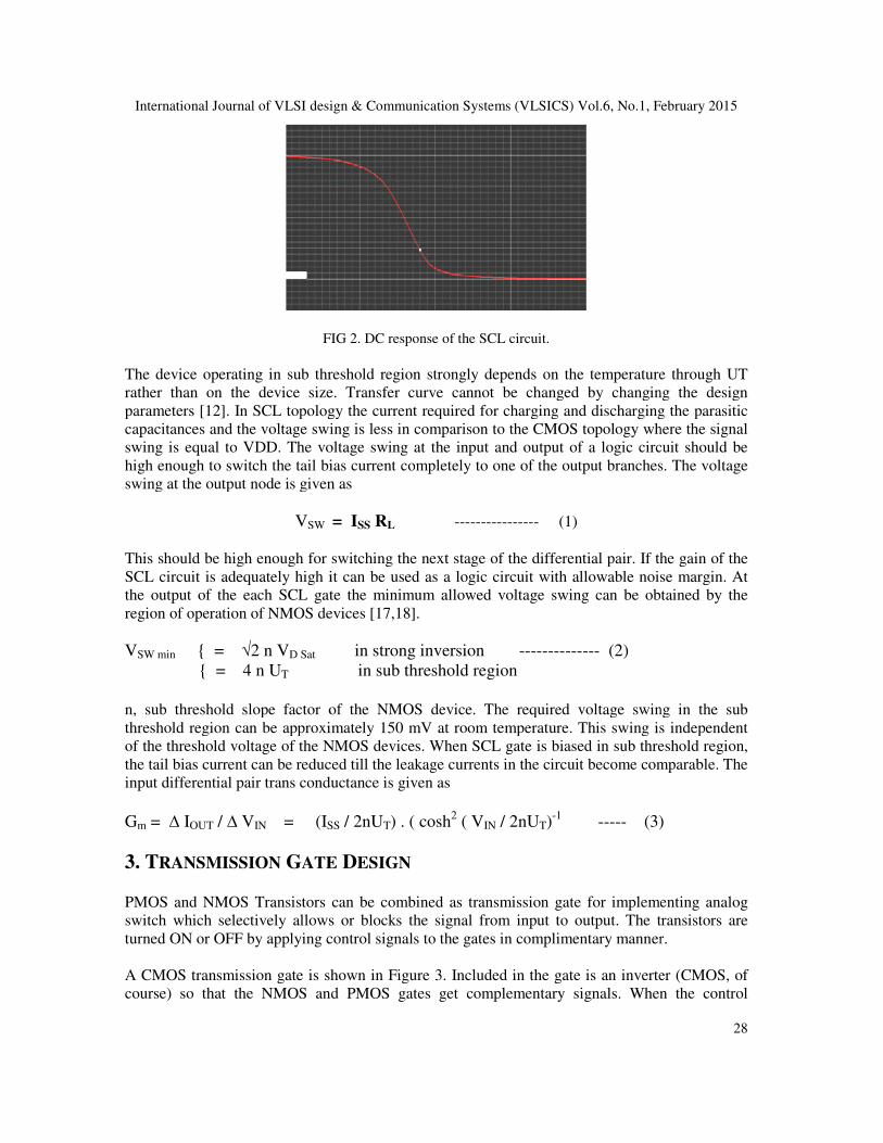
FIG 2. DC response of the SCL circuit.
The device operating in sub threshold region strongly depends on the temperature through UT
rather than on the device size. Transfer curve cannot be changed by changing the design
parameters [12]. In SCL topology the current required for charging and disch
capacitances and the voltage swing is less in comparison to the CMOS topology where the signal
swing is equal to VDD. The voltage swing at the input and output of a logic circuit should be
high enough to switch the tail bias current co
swing at the output node is given as
VSW
This should be high enough for switching the next stage of the differential pair. If the gain of the
SCL circuit is adequately high it can be used as a logic circuit with allowable noise margin. At
the output of the each SCL gate the minimum allowed voltage swing can be obtained by the
region of operation of NMOS devices [17,18].
VSW min { = √2 n VD Sat
{ = 4 n UT
n, sub threshold slope factor of the NMOS device. The required voltage swing in the sub
threshold region can be approximately 150
of the threshold voltage of the NMOS devices.
the tail bias current can be reduced till the leakage currents in the circuit become comparable. The
input differential pair trans conductance is given as
Gm = ∆ IOUT / ∆ VIN = (ISS
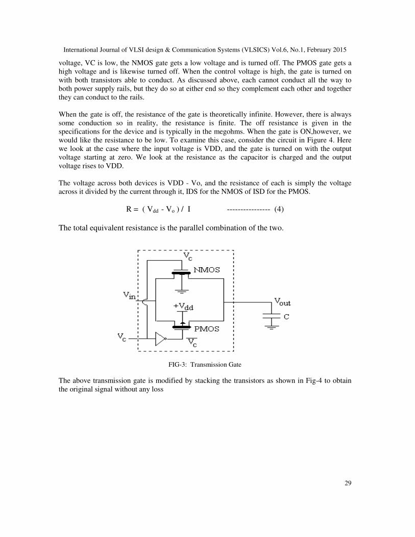
3. TRANSMISSION GATE
PMOS and NMOS Transistors can be combined as transmission gate for implementing analog
switch which selectively allows or blocks the signal from input to output. The transistors are
turned ON or OFF by applying control signals to the gates in complimentary manner.
A CMOS transmission gate is shown in Figure 3. Included in the gate is an inv
course) so that the NMOS and PMOS gates get complementary signals. When the control
International Journal of VLSI design & Communication Systems (VLSICS) Vol.6, No.1, February 2015
FIG 2. DC response of the SCL circuit.
The device operating in sub threshold region strongly depends on the temperature through UT
rather than on the device size. Transfer curve cannot be changed by changing the design
parameters [12]. In SCL topology the current required for charging and discharging the parasitic
capacitances and the voltage swing is less in comparison to the CMOS topology where the signal
swing is equal to VDD. The voltage swing at the input and output of a logic circuit should be
high enough to switch the tail bias current completely to one of the output branches. The voltage
swing at the output node is given as
= ISS RL ---------------- (1)
This should be high enough for switching the next stage of the differential pair. If the gain of the
t is adequately high it can be used as a logic circuit with allowable noise margin. At
the output of the each SCL gate the minimum allowed voltage swing can be obtained by the
region of operation of NMOS devices [17,18].
in strong inversion -------------- (2)
in sub threshold region
n, sub threshold slope factor of the NMOS device. The required voltage swing in the sub
threshold region can be approximately 150 mV at room temperature. This swing is independent
of the threshold voltage of the NMOS devices. When SCL gate is biased in sub threshold region,
the tail bias current can be reduced till the leakage currents in the circuit become comparable. The
erential pair trans conductance is given as
SS / 2nUT) . ( cosh2 ( VIN / 2nUT)
-1 ----- (3)
ATE DESIGN
PMOS and NMOS Transistors can be combined as transmission gate for implementing analog
switch which selectively allows or blocks the signal from input to output. The transistors are
turned ON or OFF by applying control signals to the gates in complimentary manner.
A CMOS transmission gate is shown in Figure 3. Included in the gate is an inverter (CMOS, of
course) so that the NMOS and PMOS gates get complementary signals. When the control
International Journal of VLSI design & Communication Systems (VLSICS) Vol.6, No.1, February 2015
28
The device operating in sub threshold region strongly depends on the temperature through UT
rather than on the device size. Transfer curve cannot be changed by changing the design
arging the parasitic
capacitances and the voltage swing is less in comparison to the CMOS topology where the signal
swing is equal to VDD. The voltage swing at the input and output of a logic circuit should be
mpletely to one of the output branches. The voltage
This should be high enough for switching the next stage of the differential pair. If the gain of the
t is adequately high it can be used as a logic circuit with allowable noise margin. At
the output of the each SCL gate the minimum allowed voltage swing can be obtained by the
n, sub threshold slope factor of the NMOS device. The required voltage swing in the sub
mV at room temperature. This swing is independent
When SCL gate is biased in sub threshold region,
the tail bias current can be reduced till the leakage currents in the circuit become comparable. The
(3)
PMOS and NMOS Transistors can be combined as transmission gate for implementing analog
switch which selectively allows or blocks the signal from input to output. The transistors are
turned ON or OFF by applying control signals to the gates in complimentary manner.
erter (CMOS, of
course) so that the NMOS and PMOS gates get complementary signals. When the control
International Journal of VLSI design & Communication Systems (VLSICS) Vol.6, No.1, February 2015
29
voltage, VC is low, the NMOS gate gets a low voltage and is turned off. The PMOS gate gets a
high voltage and is likewise turned off. When the control voltage is high, the gate is turned on
with both transistors able to conduct. As discussed above, each cannot conduct all the way to
both power supply rails, but they do so at either end so they complement each other and together
they can conduct to the rails.
When the gate is off, the resistance of the gate is theoretically infinite. However, there is always
some conduction so in reality, the resistance is finite. The off resistance is given in the
specifications for the device and is typically in the megohms. When the gate is ON,however, we
would like the resistance to be low. To examine this case, consider the circuit in Figure 4. Here
we look at the case where the input voltage is VDD, and the gate is turned on with the output
voltage starting at zero. We look at the resistance as the capacitor is charged and the output
voltage rises to VDD.
The voltage across both devices is VDD - Vo, and the resistance of each is simply the voltage
across it divided by the current through it, IDS for the NMOS of ISD for the PMOS.
R = ( Vdd - Vo ) / I ---------------- (4)
The total equivalent resistance is the parallel combination of the two.
FIG-3: Transmission Gate
The above transmission gate is modified by stacking the transistors as shown in Fig-4 to obtain
the original signal without any loss
International Journal of VLSI design & Communication Systems (VLSICS) Vol.6, No.1, February 2015
30
Fig: 4. Modified Transmission gate
The stacking of transistors improves the aspect ratio, performance and ON resistance. The
transistor widths are maintained in the ratio 1:2 for NMOS to PMOS. The performance varies
largely because of stacking as the variation almost doubles with two fingers than that of a single
transistor.
4. DYNAMIC THRESHOLD TRANSMISSION GATE
Body bias effect is normally studied in the reverse bias regime, where threshold voltage increases
as body-to-source reverse bias is made larger. DTMOS operates in the exact opposite regime.
Namely, the body-source junction is “forward biased” (at less than 0.6 V), forcing the threshold
voltage to drop.
Vth = 2ΦB + VFB + ( 2εSqNa(2ΦB )1/2
-------------------- ----------------- (5)
COX
The transistor threshold voltage Vt changes with the difference of voltage between Source and
bulk VSB. The bulk is treated as a second gate because VSB effects threshold voltage Vt which
helps in identifying the switching behavior of the transistor. The body effect is measured in terms
of body coefficient γγγγ(gamma). The threshold voltage of the Transistor is given as
Vth = VTh0 + γB ( |2ΦF + VSB|)1/2
- |2 ΦF| )1/2
----------------- (6)
where φF is the bulk Fermi- potential ,VTh0 is the threshold voltage when VSB=0 and γB is the
body-effect coefficient. Therefore the threshold voltage can be varied by dynamically by varying
VSB which forms DTMOS transistor. Typically, the source and body is either zero biased or
reverse biased. The performance of the circuits can be improved by lowering the threshold
voltage by applying forward body bias [10]. The transmission gate is designed using this concept
and is shown in FIG 5.
International Journal of VLSI design & Communication Systems (VLSICS) Vol.6, No.1, February 2015
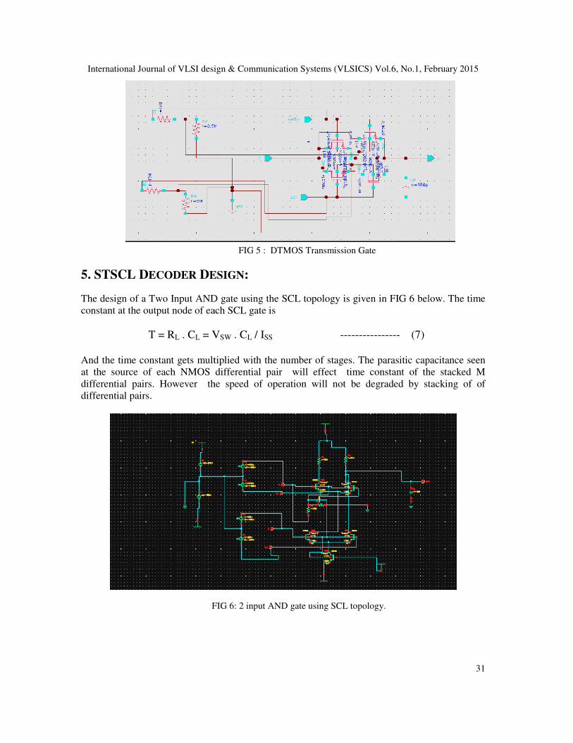
5. STSCL DECODER DESIGN
The design of a Two Input AND gate using the SCL topology is given in FIG 6 below. The time
constant at the output node of each SCL gate is
T = RL . CL = V
And the time constant gets multiplied with the number of stages. The parasitic capacitance seen
at the source of each NMOS differential pair will effect time constant of the sta
differential pairs. However the speed of operation will not be degraded by stacking of of
differential pairs.
FIG 6: 2 input AND gate using SCL topology.
International Journal of VLSI design & Communication Systems (VLSICS) Vol.6, No.1, February 2015
FIG 5 : DTMOS Transmission Gate
ESIGN:
The design of a Two Input AND gate using the SCL topology is given in FIG 6 below. The time
constant at the output node of each SCL gate is
= VSW . CL / ISS ---------------- (7)
And the time constant gets multiplied with the number of stages. The parasitic capacitance seen
at the source of each NMOS differential pair will effect time constant of the sta
differential pairs. However the speed of operation will not be degraded by stacking of of
FIG 6: 2 input AND gate using SCL topology.
International Journal of VLSI design & Communication Systems (VLSICS) Vol.6, No.1, February 2015
31
The design of a Two Input AND gate using the SCL topology is given in FIG 6 below. The time
And the time constant gets multiplied with the number of stages. The parasitic capacitance seen
at the source of each NMOS differential pair will effect time constant of the stacked M
differential pairs. However the speed of operation will not be degraded by stacking of of
International Journal of VLSI design & Communication Systems (VLSICS) Vol.6, No.1, February 2015
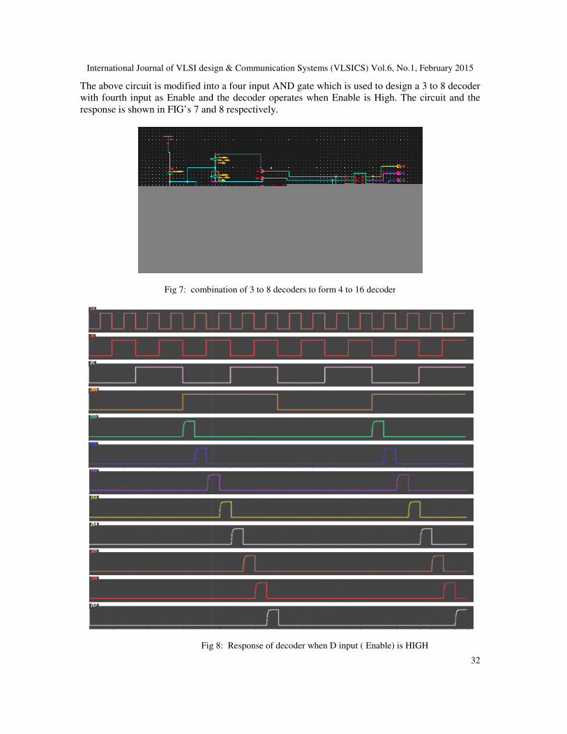
The above circuit is modified into a four input AND gate which is used to design a
with fourth input as Enable and the decoder operates when Enable is High. The circuit and the
response is shown in FIG’s 7 and 8 respectively.
Fig 7: combination of 3 to 8 decoders to form 4 to 16 decoder
Fig 8: Response of decod
International Journal of VLSI design & Communication Systems (VLSICS) Vol.6, No.1, February 2015
The above circuit is modified into a four input AND gate which is used to design a 3 to 8 decoder
with fourth input as Enable and the decoder operates when Enable is High. The circuit and the
response is shown in FIG’s 7 and 8 respectively.
Fig 7: combination of 3 to 8 decoders to form 4 to 16 decoder
Fig 8: Response of decoder when D input ( Enable) is HIGH
International Journal of VLSI design & Communication Systems (VLSICS) Vol.6, No.1, February 2015
32
3 to 8 decoder
with fourth input as Enable and the decoder operates when Enable is High. The circuit and the
er when D input ( Enable) is HIGH
International Journal of VLSI design & Communication Systems (VLSICS) Vol.6, No.1, February 2015
33
6. MULTIPLEXER DESIGN
In the past the multiplexers are designed using the concept of shift registers which are built by
synchronously triggered D flip flops with external clock. The major disadvantage of this circuit is
the clock feed through to the output line and moreover glitches occur for every positive and
negative clock edge. This problem has been reduced in the proposed multiplexer design.
In place of the static body bias used once either during design or at production the dynamic body
bias can be utilized which changes many times and also reduces the temperature and aging
effects. The DBB minimizes the temperature and aging effects and also for optimizing very low
power operation the power management modes are utilized effectively [7, 8]
In FIG 4 the NMOS and PMOS transistors will turn ON by the SEL and the complimentary
SELBR signal and the input signal will be allowed to pass to the output. Complimentarily both
the transistors will turn OFF when SEL is at logic ‘0’ and the input signal will be blocked. During
the transition period the output will be forced to high impedance state from ON to OFF and
during this state small dc voltage will appear at the output due to charging of the junction
capacitance. This is reduced by connecting a PMOS transistor between the output and ground
which turns ON when all transistors are OFF forcing the output to ground.
The NMOS and PMOS transistor widths are maintained in the ratio of 1:2 and the ON resistance
Ron of the transmission gate is given as
…….. (8)
The overdrive voltage, Vov = Vgs – Vth and the aspect ratio W/L decide the value of Ron. The ON
resistance of 27 ohms and OFF resistance of 10Mohms were obtained with very low leakage
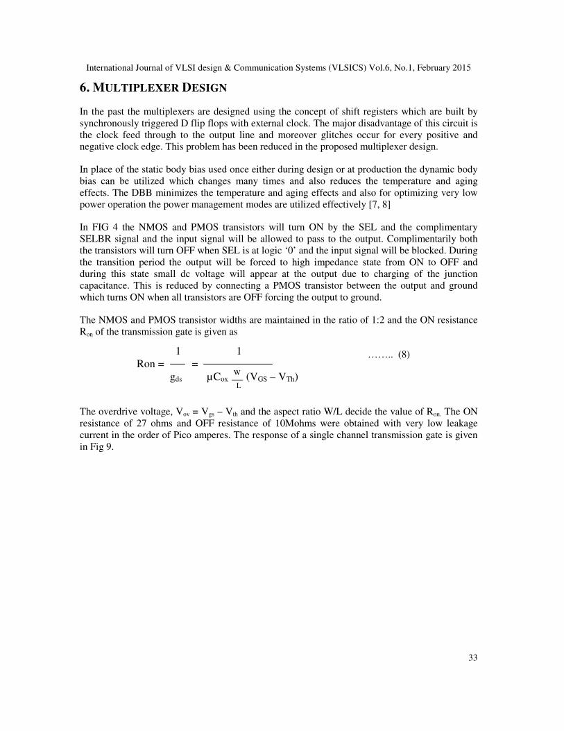
current in the order of Pico amperes. The response of a single channel transmission gate is given
in Fig 9.
1 1
Ron = =
gds µCox W
(VGS – VTh)
L
International Journal of VLSI design & Communication Systems (VLSICS) Vol.6, No.1, February 2015
Fig 9: Response of single channel Transmission gate
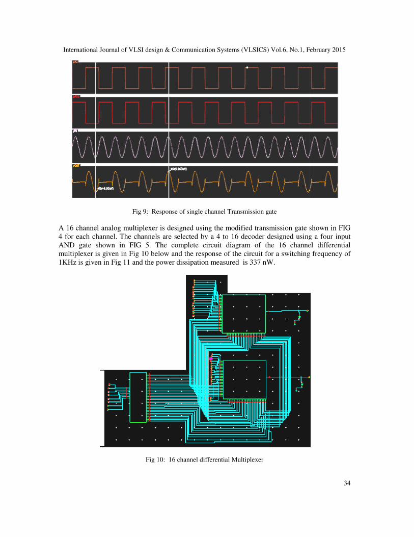
A 16 channel analog multiplexer is designed using the modified transmission gate shown in FIG
4 for each channel. The channels are selected by a 4 to 16 decoder designed using a four input
AND gate shown in FIG 5. The complete circuit diagram of the 16 channel differential
multiplexer is given in Fig 10 below and the response of the circuit for a switching frequency of
1KHz is given in Fig 11 and the power dissipation measured is 337 nW.
Fig 10: 16 channel differential Multiplexer
International Journal of VLSI design & Communication Systems (VLSICS) Vol.6, No.1, February 2015
Fig 9: Response of single channel Transmission gate
multiplexer is designed using the modified transmission gate shown in FIG
4 for each channel. The channels are selected by a 4 to 16 decoder designed using a four input
AND gate shown in FIG 5. The complete circuit diagram of the 16 channel differential
ltiplexer is given in Fig 10 below and the response of the circuit for a switching frequency of
1KHz is given in Fig 11 and the power dissipation measured is 337 nW.
Fig 10: 16 channel differential Multiplexer
International Journal of VLSI design & Communication Systems (VLSICS) Vol.6, No.1, February 2015
34
multiplexer is designed using the modified transmission gate shown in FIG
4 for each channel. The channels are selected by a 4 to 16 decoder designed using a four input
AND gate shown in FIG 5. The complete circuit diagram of the 16 channel differential
ltiplexer is given in Fig 10 below and the response of the circuit for a switching frequency of
International Journal of VLSI design & Communication Systems (VLSICS) Vol.6, No.1, February 2015
35
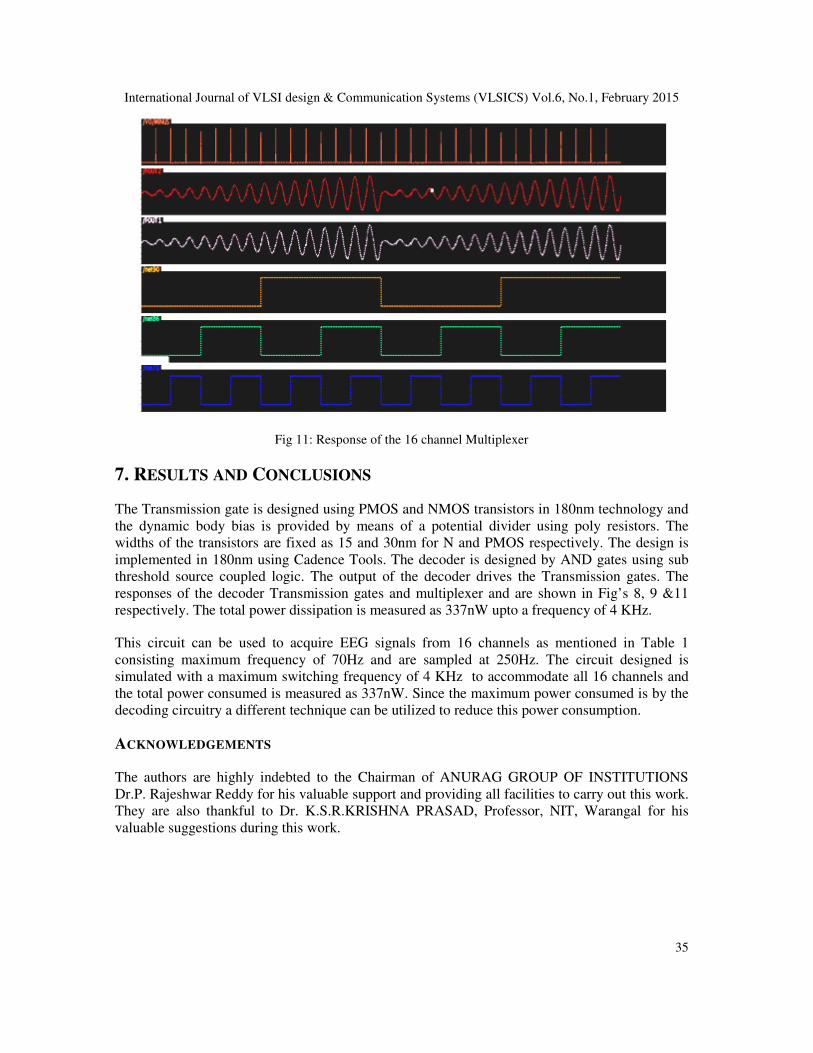
Fig 11: Response of the 16 channel Multiplexer
7. RESULTS AND CONCLUSIONS
The Transmission gate is designed using PMOS and NMOS transistors in 180nm technology and
the dynamic body bias is provided by means of a potential divider using poly resistors. The
widths of the transistors are fixed as 15 and 30nm for N and PMOS respectively. The design is
implemented in 180nm using Cadence Tools. The decoder is designed by AND gates using sub
threshold source coupled logic. The output of the decoder drives the Transmission gates. The
responses of the decoder Transmission gates and multiplexer and are shown in Fig’s 8, 9 &11
respectively. The total power dissipation is measured as 337nW upto a frequency of 4 KHz.
This circuit can be used to acquire EEG signals from 16 channels as mentioned in Table 1
consisting maximum frequency of 70Hz and are sampled at 250Hz. The circuit designed is
simulated with a maximum switching frequency of 4 KHz to accommodate all 16 channels and
the total power consumed is measured as 337nW. Since the maximum power consumed is by the
decoding circuitry a different technique can be utilized to reduce this power consumption.
ACKNOWLEDGEMENTS
The authors are highly indebted to the Chairman of ANURAG GROUP OF INSTITUTIONS
Dr.P. Rajeshwar Reddy for his valuable support and providing all facilities to carry out this work.
They are also thankful to Dr. K.S.R.KRISHNA PRASAD, Professor, NIT, Warangal for his
valuable suggestions during this work.
International Journal of VLSI design & Communication Systems (VLSICS) Vol.6, No.1, February 2015
36
REFERENCES
[1] M. Horowitz et al., “Low-power digital design,” in Proc. IEEE Int.Symp. Low Power Electronics and
Design (ISLPED), 1994, pp. 8–11.
[2] D. Suvakovic and C. A. T. Salama, “A low Vt CMOS implantation of an LPLV digital filter core for
portable audio applications,” IEEE Trans. Circuits Syst. II, Analog Digit. Signal process., vol. 47, no.
11,pp. 1297–1300, Nov. 2000.
[3] G. Gielen, “Ultra-low-power sensor networks in nanometer CMOS,” in Int. Symp. Signals, Circuits
and Systems (ISSCS), Jul. 2007, vol. 1,pp. 1–2.
[4] B. A.Warneke and K. S. J. Pister, “An ultra-low energy microcontroller for smart dust wireless sensor
networks,” in IEEE Int. Solid-State Circuits Conf. (ISSCC) Dig. Tech. Papers, 2004, pp. 316–317.
[5] L. S. Wong et al., “A very low-power CMOS mixed-signal IC for implantable pacemaker
applications,” IEEE J. Solid-State Circuits, vol.39, no. 12, pp. 2446–2456, Dec. 2004.
[6] C. Enz and E. Vittoz, Charge-Based MOS Transistor Modeling: TheEKV Model for Low-Power and
RF IC Design. New York: Wiley,2006.
[7] C. Enz, F. Krummenacher, and E. Vittoz, “An analytical MOS transistor model valid in all regions of
operation and dedicated to lowvoltage and low-current applications,” Analog Integr. Circuits Signal
Process. J., vol. 8, pp. 83–114, Jun. 1995.
[8] C. Enz, M. Punzenberger, and D. Python, “Low-voltage log-domain signal processing in CMOS and
BiCMOS,” IEEE Trans. Circuits Syst. II, Analog Digit. Signal Process., vol. 46, no. 3, pp. 279–289,
Mar.1999.
[9] B. H. Calhoun, A. Wang, and A. Chandrakasan, “Modeling and sizing for minimum energy operation
in subthreshold circuits,” IEEE J. Solid-State Circuits, vol. 40, no. 9, pp. 1778–1786, Sep. 2005.
[10] B. H. Calhoun and A. Chandrakasan, “Ultra-dynamic voltage scaling (UDVS) using subthreshold
operation and local voltage dithering,”IEEE J. Solid-State Circuits, vol. 41, no. 1, pp. 238–245, Jan.
2006.
[11] R. Amirtharajah and A. Chandrakasan, “A micropower programmable DSP using approximate signal
processing based on distributed arithmetic,”IEEE J. Solid-State Circuits, vol. 39, no. 2, pp. 337–347,
Feb.2004.
[12] H. Soeleman, K. Roy, and B. C. Paul, “Robust subthreshold logic for ultra-low-power operation,”
IEEE Trans. Very Large Scale Integr.(VLSI) Syst., vol. 9, no. 1, pp. 90–99, Sep. 2001.
[13] A. Chandrakasan and R. Brodersen, “Minimizing power consumption in digital CMOS circuits,”
Proc. IEEE, vol. 83, no. 4, pp. 498–523,Apr. 1995.
[14] A. Chandrakasan and R. Brodersen, “Minimizing power consumption in digital CMOS circuits,”
Proc. IEEE, vol. 83, no. 4, pp. 498–523,Apr. 1995.
[15] Hari Priya, Dr.K.S.Rao et al “Design of ultra low power 8-channel analog multiplexer using dynamic
threshold for biosignals” International Journal of VLSI design & Communication Systems (VLSICS)
Vol.4, No.5, October 2013.
[16] Hari Priya, Dr.K.S.Rao et al “A low power front end analog multiplexing unit for 12 lead ecg signal
acquisition” International Journal of VLSI design & Communication Systems (VLSICS) Vol.5, No.3,
June 2014.
[17] P.R.Gray, P. J.Hurst, S.H. Lewis, and R.G.Meyer, Analysis and Design of Analog Integrated Circuits,
Wiely, Fourth Ed., 2000
[18] C. C. Enz and E. A. Vittoz, Charge-based MOS Transistor Modeling, Wiley, 2006
International Journal of VLSI design & Communication Systems (VLSICS) Vol.6, No.1, February 2015
37
AUTHORS
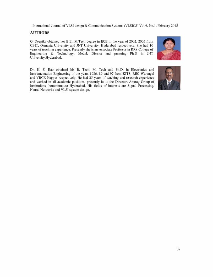
G. Deepika obtained her B.E., M.Tech degree in ECE in the year of 2002, 2005 from
CBIT, Osmania University and JNT University, Hyderabad respectively. She had 10
years of teaching experience. Presently she is an Associate Professor in RRS College of
Engineering & Technology, Medak District and pursuing Ph.D in JNT
University,Hyderabad.
Dr. K. S. Rao obtained his B. Tech, M. Tech and Ph.D. in Electronics and
Instrumentation Engineering in the years 1986, 89 and 97 from KITS, REC Warangal
and VRCE Nagpur respectively. He had 25 years of teaching and research experience
and worked in all academic positions, presently he is the Director, Anurag Group of
Institutions (Autonomous) Hyderabad. His fields of interests are Signal Processing,
Neural Networks and VLSI system design.