a 45 nm cmos-soi monolithic photonics platform with bit ...plab.colorado.edu/pub/j44.pdf · ieee...
TRANSCRIPT
IEEE JOURNAL OF SOLID-STATE CIRCUITS, VOL. 51, NO. 4, APRIL 2016 893
A 45 nm CMOS-SOI Monolithic Photonics PlatformWith Bit-Statistics-Based Resonant Microring
Thermal TuningChen Sun, Member, IEEE, Mark Wade, Michael Georgas, Sen Lin, Luca Alloatti, Benjamin Moss, Rajesh Kumar,
Amir H. Atabaki, Fabio Pavanello, Jeffrey M. Shainline, Jason S. Orcutt, Rajeev J. Ram, Fellow, IEEE,Miloš Popovic, Member, IEEE, and Vladimir Stojanovic, Member, IEEE
Abstract—The microring resonator is critical for dense wave-length division multiplexed (DWDM) chip-to-chip optical I/O,enabling modulation and channel selection at the µm-scale suit-able for a VLSI chip. Microring-based links, however, requireactive tuning to counteract process and thermo-optic variations.Here, we present a bit-statistical tuner that decouples trackingof optical one- and zero-levels to realize non-dc-balanced datatransmission, an “eye-max”-locking controller, and self-heatingcancellation without need for a high-speed sensing frontend. Weimplement the tuner on a 45 nm CMOS-SOI process with mono-lithically integrated photonic devices and circuits. The tuner con-sumes 0.74 mW in the logic while achieving a record 524 GHz(> 50 K temperature) tuning range at 3.8 µW/GHz heater effi-ciency. To our knowledge, this is the highest range and heater effi-ciency reported by an on-chip closed-loop thermal tuner to date.The tuner integrates with a 5 Gb/s 30 fJ/bit monolithic micror-ing transmitter, achieving wavelength-lock and immunity to bothtracking failures and self-heating events caused by arbitrary, non-dc-balanced bitstreams. In addition, the tuner provides criticalfunctionality for an 11-λ DWDM transmitter macro capable of11 × 8 Gb/s bandwidth on a fiber. Together with the transmit-ter, a 10 Gb/s on-chip monolithic optical receiver with 10−12 BERsensitivity of 9 µA at 10 Gb/s enables a sub-pJ/bit 5 Gb/s opticalchip-to-chip link, with the bit-statistical tuner providing thermallyrobust microring operation.
Index Terms—Microring resonator, monolithic, receiver, siliconphotonics, transceiver, thermal tuning.
Manuscript received September 09, 2015; revised November 18, 2015;accepted January 04, 2016. Date of publication March 04, 2016; date of currentversion March 29, 2016. This paper was approved by Guest Editor AndreiaCathelin. This work was supported in part by the DARPA POEM AwardHR0011-11-C-0100 and contract HR0011-11-9-0009, led by Dr. J. Shah, andin part by the NSF, Trusted Foundry, MIT CICS, Berkeley Wireless ResearchCenter, Santec, and NSERC.
C. Sun is with the Department of Electrical Engineering and ComputerScience, University of California, Berkeley, CA 94709 USA, and alsowith the Department of Electrical Engineering and Computer Science,Massachusetts Institute of Technology, Cambridge, MA 02139 USA (e-mail:[email protected]).
M. Wade, R. Kumar, F. Pavanello, J. M. Shainline, and M. Popovic are withthe Department of Electrical, Computer, and Energy Engineering, University ofColorado, Boulder, CO 80309 USA.
M. Georgas, L. Alloatti, B. Moss, A. H. Atabaki, J. S. Orcutt, and R. J.Ram are with the Department of Electrical Engineering and Computer Science,Massachusetts Institute of Technology, Cambridge, MA 02139 USA.
S. Lin and V. Stojanovic are with the Department of Electrical Engineeringand Computer Science, University of California, Berkeley, CA 94709 USA.
Color versions of one or more of the figures in this paper are available onlineat http://ieeexplore.ieee.org.
Digital Object Identifier 10.1109/JSSC.2016.2519390
I. INTRODUCTION
S ILICON photonics-enabled optical interconnect can over-come the traditional bandwidth- and power-density
tradeoffs faced by high-speed chip-to-chip electrical links [1].The ability to integrate with VLSI electronics, either mono-lithically on the same chip [2]–[4] or heterogeneously onseparate chips via three-dimensional (3-D) stacking [5], [6]or system-in-package integration [7], [8], allows silicon pho-tonics to provide a scalable interconnect for future memorysystems [9], [10], [42], high-radix network switch chips [11],and core-to-core crossbars [12], [13].
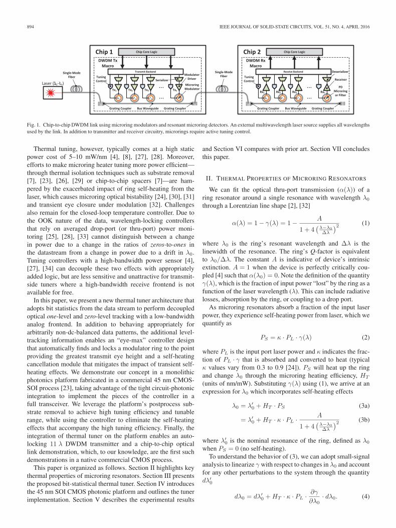
Key to the realization of bandwidth densities and energyefficiencies promised by silicon photonics is the silicon micror-ing resonator. Microrings act as µm-scale optical notch filters,rejecting wavelengths that resonate in the ring while passingwavelengths that do not. Voltages applied across microringsdoped with a p–n or p–i–n junction modulate the ring’s freecarrier concentration and shift the microring’s stop band viathe free carrier plasma dispersion effect [14], [15]. This canbe used to ON–OFF key (OOK) a carrier wavelength closeto resonance, creating a compact, CMOS-compatible [15],and channel-selective electro-optic modulator. In a receiver, amicroring performs channel selection for a broadband photode-tector (PD) or acts directly as a resonant PD [4], [16]. Theseproperties allow microrings to enable dense wavelength divi-sion multiplexing (DWDM), where multiple streams of data arecarried by closely spaced carrier wavelengths sharing a singlewaveguide or fiber (Fig. 1), on silicon chips.
Despite all these advantages, microring-based DWDM hasyet to be widely adopted due to inadequate progress on themitigation of thermal and process variations on a microring’sresonant wavelength (λ0). A typical silicon microring with Q =10, 000 and a nominal λ0 in the 1180–1550 nm (254–193 THz)band suffers > 3 dB of signal loss for a λ0 offset of just 0.1 nm.Silicon microrings experience 0.15–1.8 nm [17] of ring-to-ringλ0 variations from process variations and 0.05–0.1 nm/K [18],[19] of thermo-optic λ0 shifts (−10 GHz/K [20]), indicatingthat a microring-based link cannot tolerate even a 1 K changein temperature without active λ0 stabilization. Fortunately, thestrong thermo-optic effect enables process variations to becompensated through a temperature change of a few Kelvin,popularizing thermal tuning of λ0 through microring-embeddedresistive heaters [8], [18], [21]–[26].
0018-9200 © 2016 IEEE. Personal use is permitted, but republication/redistribution requires IEEE permission.See http://www.ieee.org/publications_standards/publications/rights/index.html for more information.
894 IEEE JOURNAL OF SOLID-STATE CIRCUITS, VOL. 51, NO. 4, APRIL 2016
Fig. 1. Chip-to-chip DWDM link using microring modulators and resonant microring detectors. An external multiwavelength laser source supplies all wavelengthsused by the link. In addition to transmitter and receiver circuitry, microrings require active tuning control.
Thermal tuning, however, typically comes at a high staticpower cost of 5–10 mW/nm [4], [8], [27], [28]. Moreover,efforts to make microring heater tuning more power efficient—through thermal isolation techniques such as substrate removal[7], [23], [26], [29] or chip-to-chip spacers [7]—are ham-pered by the exacerbated impact of ring self-heating from thelaser, which causes microring optical bistability [24], [30], [31]and transient eye closure under modulation [32]. Challengesalso remain for the closed-loop temperature controller. Due tothe OOK nature of the data, wavelength-locking controllersthat rely on averaged drop-port (or thru-port) power moni-toring [25], [28], [33] cannot distinguish between a changein power due to a change in the ratios of zeros-to-ones inthe datastream from a change in power due to a drift in λ0.Tuning controllers with a high-bandwidth power sensor [4],[27], [34] can decouple these two effects with appropriatelyadded logic, but are less sensitive and unattractive for transmit-side tuners where a high-bandwidth receive frontend is notavailable for free.
In this paper, we present a new thermal tuner architecture thatadopts bit statistics from the data stream to perform decoupledoptical one-level and zero-level tracking with a low-bandwidthanalog frontend. In addition to behaving appropriately forarbitrarily non-dc-balanced data patterns, the additional level-tracking information enables an “eye-max” controller designthat automatically finds and locks a modulator ring to the pointproviding the greatest transmit eye height and a self-heatingcancellation module that mitigates the impact of transient self-heating effects. We demonstrate our concept in a monolithicphotonics platform fabricated in a commercial 45 nm CMOS-SOI process [23], taking advantage of the tight circuit-photonicintegration to implement the pieces of the controller in afull transceiver. We leverage the platform’s postprocess sub-strate removal to achieve high tuning efficiency and tunablerange, while using the controller to eliminate the self-heatingeffects that accompany the high tuning efficiency. Finally, theintegration of thermal tuner on the platform enables an auto-locking 11 λ DWDM transmitter and a chip-to-chip opticallink demonstration, which, to our knowledge, are the first suchdemonstrations in a native commercial CMOS process.
This paper is organized as follows. Section II highlights keythermal properties of microring resonators. Section III presentsthe proposed bit-statistical thermal tuner. Section IV introducesthe 45 nm SOI CMOS photonic platform and outlines the tunerimplementation. Section V describes the experimental results
and Section VI compares with prior art. Section VII concludesthis paper.
II. THERMAL PROPERTIES OF MICRORING RESONATORS
We can fit the optical thru-port transmission (α(λ)) of aring resonator around a single resonance with wavelength λ0
through a Lorentzian line shape [2], [32]
α(λ) = 1− γ(λ) = 1− A
1 + 4(λ−λ0
Δλ
)2 (1)
where λ0 is the ring’s resonant wavelength and Δλ is thelinewidth of the resonance. The ring’s Q-factor is equivalentto λ0/Δλ. The constant A is indicative of device’s intrinsicextinction. A = 1 when the device is perfectly critically cou-pled [4] such that α(λ0) = 0. Note the definition of the quantityγ(λ), which is the fraction of input power “lost” by the ring as afunction of the laser wavelength (λ). This can include radiativelosses, absorption by the ring, or coupling to a drop port.
As microring resonators absorb a fraction of the input laserpower, they experience self-heating power from laser, which wequantify as
PS = κ · PL · γ(λ) (2)
where PL is the input port laser power and κ indicates the frac-tion of PL · γ that is absorbed and converted to heat (typicalκ values vary from 0.3 to 0.9 [24]). PS will heat up the ringand change λ0 through the microring heating efficiency, HT
(units of nm/mW). Substituting γ(λ) using (1), we arrive at anexpression for λ0 which incorporates self-heating effects
λ0 = λ′0 +HT · PS (3a)
= λ′0 +HT · κ · PL · A
1 + 4(λ−λ0
Δλ
)2 (3b)
where λ′0 is the nominal resonance of the ring, defined as λ0
when PS = 0 (no self-heating).To understand the behavior of (3), we can adopt small-signal
analysis to linearize γ with respect to changes in λ0 and accountfor any other perturbations to the system through the quantitydλ′
0
dλ0 = dλ′0 +HT · κ · PL · ∂γ
∂λ0· dλ0. (4)
SUN et al.: 45 NM CMOS-SOI MONOLITHIC PHOTONICS PLATFORM 895
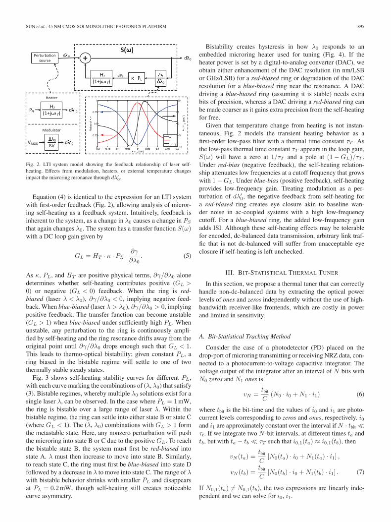
Fig. 2. LTI system model showing the feedback relationship of laser self-heating. Effects from modulation, heaters, or external temperature changesimpact the microring resonance through dλ′
0.
Equation (4) is identical to the expression for an LTI systemwith first-order feedback (Fig. 2), allowing analysis of micror-ing self-heating as a feedback system. Intuitively, feedback isinherent to the system, as a change in λ0 causes a change in PS
that again changes λ0. The system has a transfer function S(ω)with a DC loop gain given by
GL = HT · κ · PL · ∂γ
∂λ0. (5)
As κ, PL, and HT are positive physical terms, ∂γ/∂λ0 alonedetermines whether self-heating contributes positive (GL >0) or negative (GL < 0) feedback. When the ring is red-biased (laser λ < λ0), ∂γ/∂λ0 < 0, implying negative feed-back. When blue-biased (laser λ > λ0), ∂γ/∂λ0 > 0, implyingpositive feedback. The transfer function can become unstable(GL > 1) when blue-biased under sufficiently high PL. Whenunstable, any perturbation to the ring is continuously ampli-fied by self-heating and the ring resonance drifts away from theoriginal point until ∂γ/∂λ0 drops enough such that GL < 1.This leads to thermo-optical bistability; given constant PL, aring biased in the bistable regime will settle to one of twothermally stable steady states.
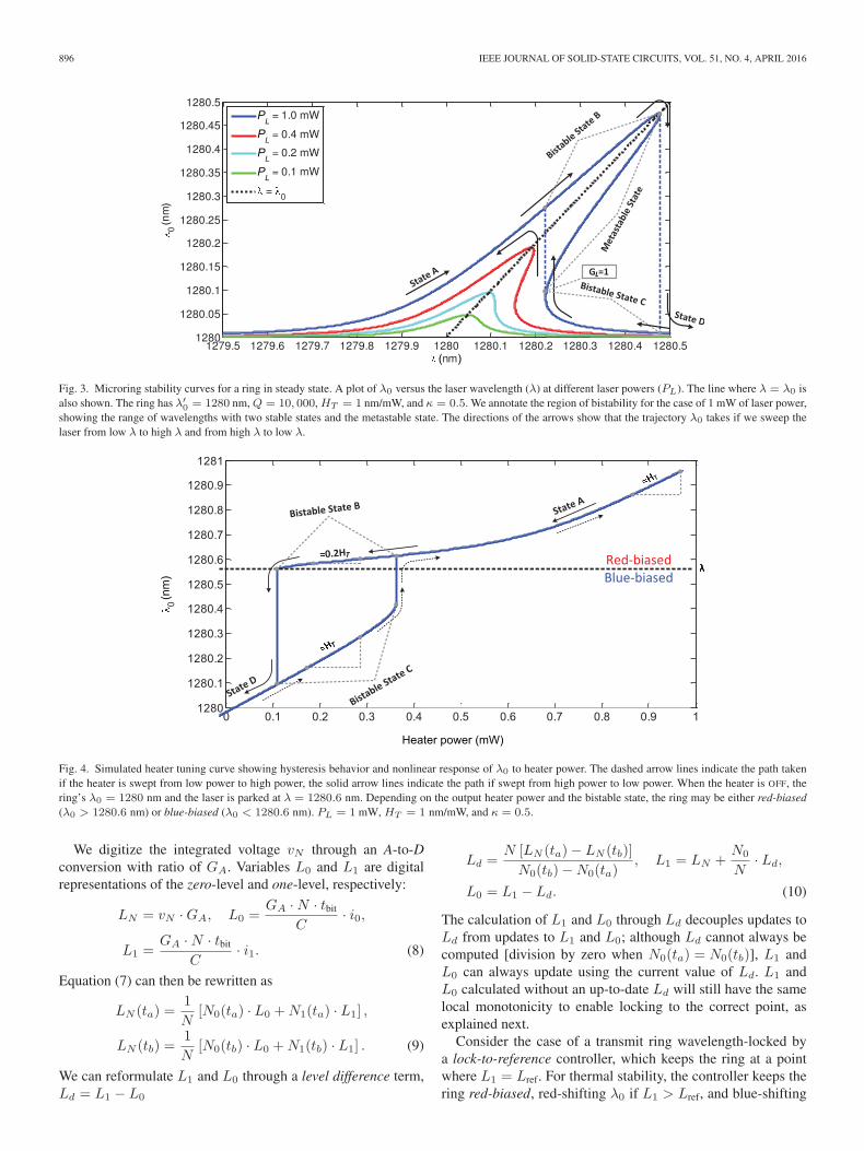
Fig. 3 shows self-heating stability curves for different PL,with each curve marking the combinations of (λ, λ0) that satisfy(3). Bistable regimes, whereby multiple λ0 solutions exist for asingle laser λ, can be observed. In the case where PL = 1mW,the ring is bistable over a large range of laser λ. Within thebistable regime, the ring can settle into either state B or state C(where GL < 1). The (λ, λ0) combinations with GL > 1 formthe metastable state. Here, any nonzero perturbation will pushthe microring into state B or C due to the positive GL. To reachthe bistable state B, the system must first be red-biased intostate A. λ must then increase to move into state B. Similarly,to reach state C, the ring must first be blue-biased into state Dfollowed by a decrease in λ to move into state C. The range of λwith bistable behavior shrinks with smaller PL and disappearsat PL = 0.2mW, though self-heating still creates noticeablecurve asymmetry.
Bistability creates hysteresis in how λ0 responds to anembedded microring heater used for tuning (Fig. 4). If theheater power is set by a digital-to-analog converter (DAC), weobtain either enhancement of the DAC resolution (in nm/LSBor GHz/LSB) for a red-biased ring or degradation of the DACresolution for a blue-biased ring near the resonance. A DACdriving a blue-biased ring (assuming it is stable) needs extrabits of precision, whereas a DAC driving a red-biased ring canbe made coarser as it gains extra precision from the self-heatingfor free.
Given that temperature change from heating is not instan-taneous, Fig. 2 models the transient heating behavior as afirst-order low-pass filter with a thermal time constant τT . Asthe low-pass thermal time constant τT appears in the loop gain,S(ω) will have a zero at 1/τT and a pole at (1−GL)/τT .Under red-bias (negative feedback), the self-heating relation-ship attenuates low frequencies at a cutoff frequency that growswith 1−GL. Under blue-bias (positive feedback), self-heatingprovides low-frequency gain. Treating modulation as a per-turbation of dλ′
0, the negative feedback from self-heating fora red-biased ring creates eye closure akin to baseline wan-der noise in ac-coupled systems with a high low-frequencycutoff. For a blue-biased ring, the added low-frequency gainadds ISI. Although these self-heating effects may be tolerablefor encoded, dc-balanced data transmission, arbitrary link traf-fic that is not dc-balanced will suffer from unacceptable eyeclosure if self-heating is left unchecked.
III. BIT-STATISTICAL THERMAL TUNER
In this section, we propose a thermal tuner that can correctlyhandle non-dc-balanced data by extracting the optical powerlevels of ones and zeros independently without the use of high-bandwidth receiver-like frontends, which are costly in powerand limited in sensitivity.
A. Bit-Statistical Tracking Method
Consider the case of a photodetector (PD) placed on thedrop-port of microring transmitting or receiving NRZ data, con-nected to a photocurrent-to-voltage capacitive integrator. Thevoltage output of the integrator after an interval of N bits withN0 zeros and N1 ones is
vN =tbit
C(N0 · i0 +N1 · i1) (6)
where tbit is the bit-time and the values of i0 and i1 are photo-current levels corresponding to zeros and ones, respectively. i0and i1 are approximately constant over the interval if N · tbit �τt. If we integrate two N -bit intervals, at different times ta andtb, but with ta − tb � τT such that i0,1(ta) ≈ i0,1(tb), then
vN (ta) =tbit
C[N0(ta) · i0 +N1(ta) · i1] ,
vN (tb) =tbit
C[N0(tb) · i0 +N1(tb) · i1] . (7)
If N0,1(ta) �= N0,1(tb), the two expressions are linearly inde-pendent and we can solve for i0, i1.
896 IEEE JOURNAL OF SOLID-STATE CIRCUITS, VOL. 51, NO. 4, APRIL 2016
()
)(
PL
PL
PL
PL
L
Fig. 3. Microring stability curves for a ring in steady state. A plot of λ0 versus the laser wavelength (λ) at different laser powers (PL). The line where λ = λ0 isalso shown. The ring has λ′
0 = 1280 nm, Q = 10, 000, HT = 1 nm/mW, and κ = 0.5. We annotate the region of bistability for the case of 1 mW of laser power,showing the range of wavelengths with two stable states and the metastable state. The directions of the arrows show that the trajectory λ0 takes if we sweep thelaser from low λ to high λ and from high λ to low λ.
Fig. 4. Simulated heater tuning curve showing hysteresis behavior and nonlinear response of λ0 to heater power. The dashed arrow lines indicate the path takenif the heater is swept from low power to high power, the solid arrow lines indicate the path if swept from high power to low power. When the heater is OFF, thering’s λ0 = 1280 nm and the laser is parked at λ = 1280.6 nm. Depending on the output heater power and the bistable state, the ring may be either red-biased(λ0 > 1280.6 nm) or blue-biased (λ0 < 1280.6 nm). PL = 1 mW, HT = 1 nm/mW, and κ = 0.5.
We digitize the integrated voltage vN through an A-to-Dconversion with ratio of GA. Variables L0 and L1 are digitalrepresentations of the zero-level and one-level, respectively:
LN = vN ·GA, L0 =GA ·N · tbit
C· i0,
L1 =GA ·N · tbit
C· i1. (8)
Equation (7) can then be rewritten as
LN (ta) =1
N[N0(ta) · L0 +N1(ta) · L1] ,
LN (tb) =1
N[N0(tb) · L0 +N1(tb) · L1] . (9)
We can reformulate L1 and L0 through a level difference term,Ld = L1 − L0
Ld =N [LN (ta)− LN (tb)]
N0(tb)−N0(ta), L1 = LN +
N0
N· Ld,
L0 = L1 − Ld. (10)
The calculation of L1 and L0 through Ld decouples updates toLd from updates to L1 and L0; although Ld cannot always becomputed [division by zero when N0(ta) = N0(tb)], L1 andL0 can always update using the current value of Ld. L1 andL0 calculated without an up-to-date Ld will still have the samelocal monotonicity to enable locking to the correct point, asexplained next.
Consider the case of a transmit ring wavelength-locked bya lock-to-reference controller, which keeps the ring at a pointwhere L1 = Lref. For thermal stability, the controller keeps thering red-biased, red-shifting λ0 if L1 > Lref, and blue-shifting
SUN et al.: 45 NM CMOS-SOI MONOLITHIC PHOTONICS PLATFORM 897
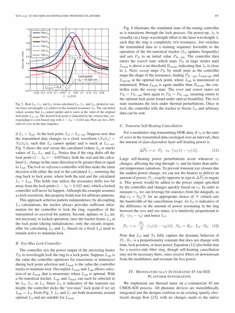
Fig. 5. Real L0, L1, and Ld versus calculated L0, L1, and Ld, plotted at vari-ous laser wavelengths (λ) relative to the nominal resonance λ0. The calculatedvalues assume that Ld cannot update and is stuck at the value of the originallock point Ld−ref. The desired lock point is indicated by the vertical line, cor-responding to a red-biased ring with λ− λ0 = 0.025 nm. Plots are for a 50%ratio of zeros in the data sequence.
if L1 < Lref. At the lock point, Ld = Ld−ref. Suppose now thatthe transmitted data changes to a clock waveform (N0(ta) =N0(tb)), such that Ld cannot update and is stuck at Ld−ref.Fig. 5 shows the real versus the calculated (where Ld is stuck)values of L0, L1, and Ld. Notice that if the ring drifts off thelock point (λ− λ0 = − 0.025nm), both the real and the calcu-lated L1 change in the same direction to be greater than or equalto Lref. The lock-to-reference controller will thus make the samedecision with either the real or the calculated L1, returning thering back to lock point, where both the real and the calculatedL1 = Lref. This holds true unless the resonance drifts too faraway from the lock point (λ− λ0 > 0.025 nm), which a lockedcontroller will never let happen. Although the example assumesa clock waveform, this property holds true for arbitrary patterns.
This approach achieves pattern independence; by decouplingLd calculations, the tracker always provides sufficient infor-mation for the controller to lock the ring, regardless of thetransmitted or received bit pattern. Second, updates to Ld arenot necessary in locked operation; once the tracker learns Ld atthe lock point (during initialization), only the circuits respon-sible for calculating L0 and L1 (based on a fixed Ld) need toremain active to maintain lock.
B. Eye-Max Lock Controller
The controller sets the power output of the microring heaterPH to wavelength-lock the ring to a lock point. Suppose Lopt isthe value the controller optimizes for (maximize or minimize)during lock point selection and Ltrack is the value the controllertracks to maintain lock. Decoupled Ltrack and Lopt allows selec-tion of an Ltrack that is monotonic where Lopt is optimal. Witha bit-statistical tracker, Lopt and Ltrack can each be selected tobe L0, L1, or Ld. Since Ld is indicative of the transmit eyeheight, the controller picks the “eye-max” lock point if we setLopt = Ld. From Fig. 5, L0 and L1 are both monotonic aroundoptimal Ld and are suitable for Ltrack.
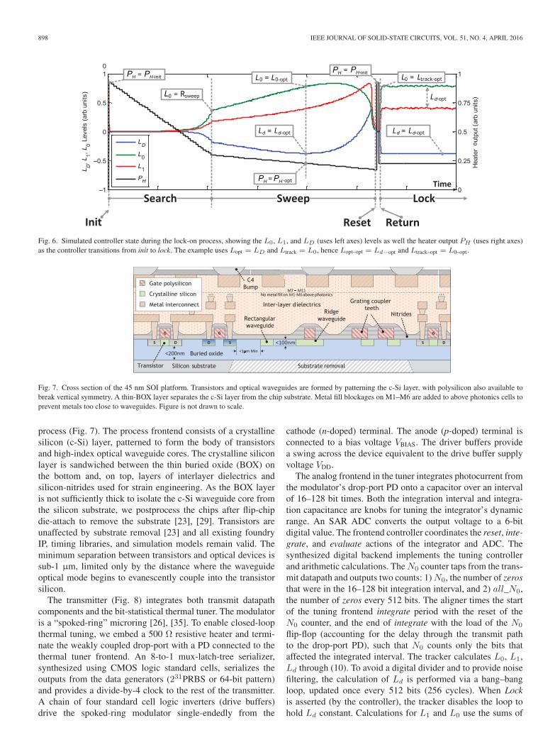
Fig. 6 illustrates the simulated state of the tuning controlleras it transitions through the lock process. On power-up, λ0 is(usually) at a large wavelength offset to the laser wavelength λ,such that the ring is completely OFF-resonance. Init switchesthe transmitted data to a training sequence favorable to theoperation of the bit-statistical tracker (Ld updates frequently)and sets PH to an initial value PH−init. The controller thenenters the search state which steps PH in large strides untilLtrack is above a set threshold Rsweep, indicating that λ0 is closeto λ. Next, sweep steps PH by small steps as the controllermaps the shape of the resonance, finding PH−opt, Ltrack-opt, andLopt-opt at the optimal lock point, where Lopt is maximized orminimized. When Ltrack is again smaller than Rsweep, the con-troller exits the sweep state. The reset and return states setPH = PH−init then again to PH = PH−opt, ensuring return tothe optimal lock point found under optical bistability. The lockstate maintains the lock under thermal perturbations. Once inlock, the controller tells the tracker to freeze Ld and arbitrarydata can be sent.
C. Transient Self-Heating Cancellation
For a modulator ring transmitting OOK data, if r0 is the ratioof zeros in the transmitted data (averaged over an interval), thenthe amount of data-dependent laser self-heating power is
ΔPS = κ · PL · r0 · [γ0(λ)− γ1(λ)] . (11)
Large self-heating power perturbations occur whenever r0changes, affecting the ring through τT and far faster than ambi-ent temperature variations. To prevent transient eye closure duethe sudden power change, we can use the heaters to deliver anamount of power, PC , exactly opposite in sign to ΔPS to negateit. This power would be added to the power output specifiedby the controller and changes quickly based on r0. In order tomeasure r0, we can leverage bit-statistics from the datapath, sothat r0 = N0/N for an appropriate choice of N (which setsthe bandwidth of the cancellation loop). As Ld is indicative ofthe difference in the amount of power resonating in the ringbetween the zero and one states, it is intuitively proportional toPL · (γ1 − γ0) and hence LD
PC = κ · PL
N· [γ1(λ)− γ0(λ)] ·N0. = KC · Ld ·N0. (12)
Note that LD and N0 fully capture the dynamic behavior ofPC .KC is a proportionality constant that does not change withtime, lock position, or laser power. Equation (12) also holds truefor a receive-side filter ring, though self-heating cancellationmay not be necessary there, since receive filters sit downstreamfrom the modulators and resonate far less power.
IV. MONOLITHICALLY INTEGRATED 45 NM SOIPLATFORM INTEGRATION
We implement our thermal tuner on a commercial 45 nmCMOS-SOI process. All photonic devices are monolithicallyintegrated and the designs conform to an existing (purely elec-trical) design flow [23], with no changes made to the native
898 IEEE JOURNAL OF SOLID-STATE CIRCUITS, VOL. 51, NO. 4, APRIL 2016
Fig. 6. Simulated controller state during the lock-on process, showing the L0, L1, and LD (uses left axes) levels as well the heater output PH (uses right axes)as the controller transitions from init to lock. The example uses Lopt = LD and Ltrack = L0, hence Lopt–opt = Ld−opt and Ltrack–opt = L0–opt.
Fig. 7. Cross section of the 45 nm SOI platform. Transistors and optical waveguides are formed by patterning the c-Si layer, with polysilicon also available tobreak vertical symmetry. A thin-BOX layer separates the c-Si layer from the chip substrate. Metal fill blockages on M1–M6 are added to above photonics cells toprevent metals too close to waveguides. Figure is not drawn to scale.
process (Fig. 7). The process frontend consists of a crystallinesilicon (c-Si) layer, patterned to form the body of transistorsand high-index optical waveguide cores. The crystalline siliconlayer is sandwiched between the thin buried oxide (BOX) onthe bottom and, on top, layers of interlayer dielectrics andsilicon-nitrides used for strain engineering. As the BOX layeris not sufficiently thick to isolate the c-Si waveguide core fromthe silicon substrate, we postprocess the chips after flip-chipdie-attach to remove the substrate [23], [29]. Transistors areunaffected by substrate removal [23] and all existing foundryIP, timing libraries, and simulation models remain valid. Theminimum separation between transistors and optical devices issub-1 µm, limited only by the distance where the waveguideoptical mode begins to evanescently couple into the transistorsilicon.
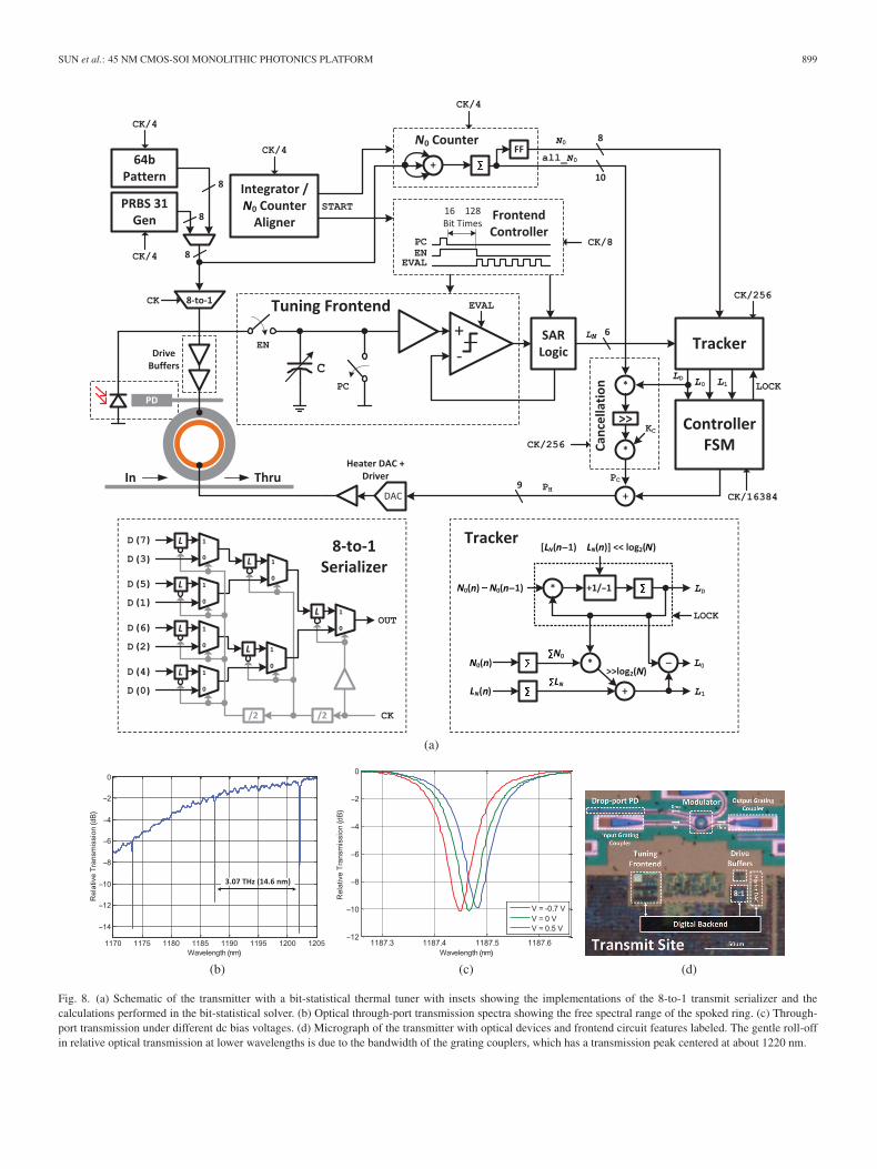
The transmitter (Fig. 8) integrates both transmit datapathcomponents and the bit-statistical thermal tuner. The modulatoris a “spoked-ring” microring [26], [35]. To enable closed-loopthermal tuning, we embed a 500 Ω resistive heater and termi-nate the weakly coupled drop-port with a PD connected to thethermal tuner frontend. An 8-to-1 mux-latch-tree serializer,synthesized using CMOS logic standard cells, serializes theoutputs from the data generators (231PRBS or 64-bit pattern)and provides a divide-by-4 clock to the rest of the transmitter.A chain of four standard cell logic inverters (drive buffers)drive the spoked-ring modulator single-endedly from the
cathode (n-doped) terminal. The anode (p-doped) terminal isconnected to a bias voltage VBIAS. The driver buffers providea swing across the device equivalent to the drive buffer supplyvoltage VDD.
The analog frontend in the tuner integrates photocurrent fromthe modulator’s drop-port PD onto a capacitor over an intervalof 16–128 bit times. Both the integration interval and integra-tion capacitance are knobs for tuning the integrator’s dynamicrange. An SAR ADC converts the output voltage to a 6-bitdigital value. The frontend controller coordinates the reset, inte-grate, and evaluate actions of the integrator and ADC. Thesynthesized digital backend implements the tuning controllerand arithmetic calculations. The N0 counter taps from the trans-mit datapath and outputs two counts: 1) N0, the number of zerosthat were in the 16–128 bit integration interval, and 2) all_N0,the number of zeros every 512 bits. The aligner times the startof the tuning frontend integrate period with the reset of theN0 counter, and the end of integrate with the load of the N0
flip-flop (accounting for the delay through the transmit pathto the drop-port PD), such that N0 counts only the bits thataffected the integrated interval. The tracker calculates L0, L1,Ld through (10). To avoid a digital divider and to provide noisefiltering, the calculation of Ld is performed via a bang–bangloop, updated once every 512 bits (256 cycles). When Lockis asserted (by the controller), the tracker disables the loop tohold Ld constant. Calculations for L1 and L0 use the sums of
SUN et al.: 45 NM CMOS-SOI MONOLITHIC PHOTONICS PLATFORM 899
Fig. 8. (a) Schematic of the transmitter with a bit-statistical thermal tuner with insets showing the implementations of the 8-to-1 transmit serializer and thecalculations performed in the bit-statistical solver. (b) Optical through-port transmission spectra showing the free spectral range of the spoked ring. (c) Through-port transmission under different dc bias voltages. (d) Micrograph of the transmitter with optical devices and frontend circuit features labeled. The gentle roll-offin relative optical transmission at lower wavelengths is due to the bandwidth of the grating couplers, which has a transmission peak centered at about 1220 nm.
900 IEEE JOURNAL OF SOLID-STATE CIRCUITS, VOL. 51, NO. 4, APRIL 2016
Fig. 9. (a) Schematic of the receiver frontend and deserializer. (b) Structure of the SiGe PD. (c) Micrograph of the receiver receiver site.
LN and N0 over 64 integration intervals in place of individualLN and N0 samples. The “eye-max” controller makes heatingchoices at a decision rate of once every 215 to 231 bits. Logicfor heating cancellation follows (12) and produces cancellationpower offsets, PC , which is added to the heater output of thecontroller to form the 9 bit digital heating code PH . The heaterdriver DAC converts PH to power dissipated by the embeddedmicroring heater.
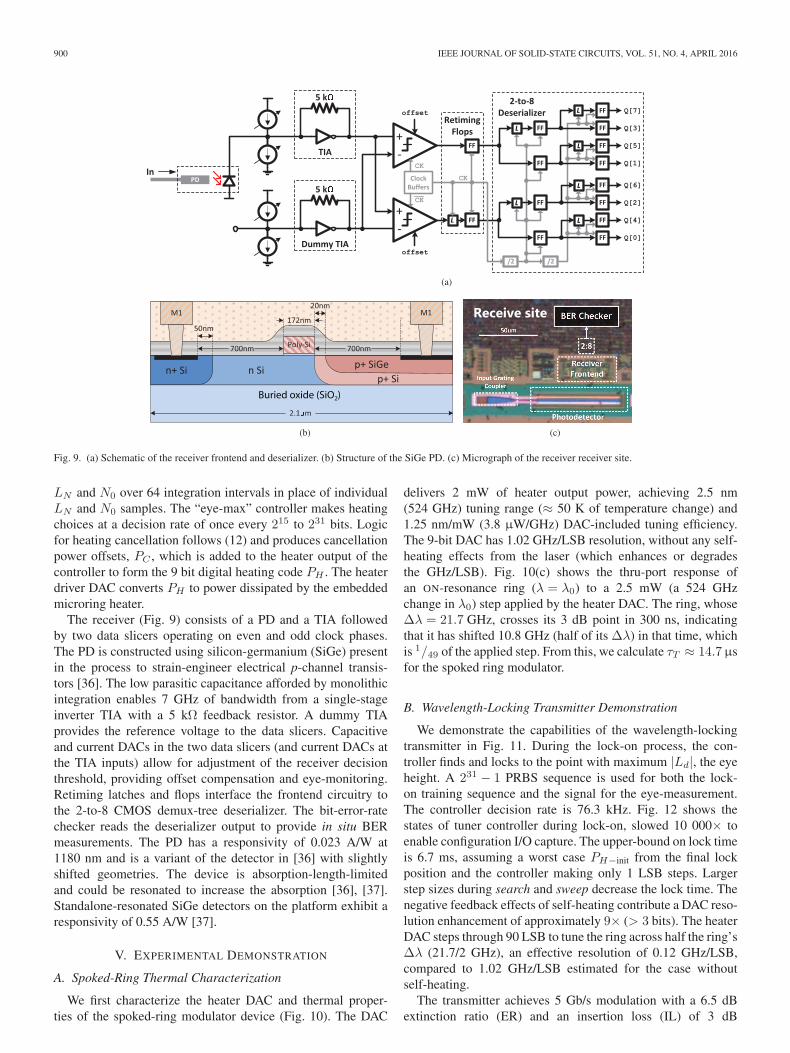
The receiver (Fig. 9) consists of a PD and a TIA followedby two data slicers operating on even and odd clock phases.The PD is constructed using silicon-germanium (SiGe) presentin the process to strain-engineer electrical p-channel transis-tors [36]. The low parasitic capacitance afforded by monolithicintegration enables 7 GHz of bandwidth from a single-stageinverter TIA with a 5 kΩ feedback resistor. A dummy TIAprovides the reference voltage to the data slicers. Capacitiveand current DACs in the two data slicers (and current DACs atthe TIA inputs) allow for adjustment of the receiver decisionthreshold, providing offset compensation and eye-monitoring.Retiming latches and flops interface the frontend circuitry tothe 2-to-8 CMOS demux-tree deserializer. The bit-error-ratechecker reads the deserializer output to provide in situ BERmeasurements. The PD has a responsivity of 0.023 A/W at1180 nm and is a variant of the detector in [36] with slightlyshifted geometries. The device is absorption-length-limitedand could be resonated to increase the absorption [36], [37].Standalone-resonated SiGe detectors on the platform exhibit aresponsivity of 0.55 A/W [37].
V. EXPERIMENTAL DEMONSTRATION
A. Spoked-Ring Thermal Characterization
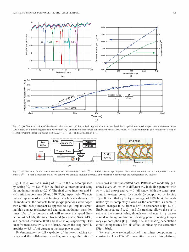
We first characterize the heater DAC and thermal proper-ties of the spoked-ring modulator device (Fig. 10). The DAC
delivers 2 mW of heater output power, achieving 2.5 nm(524 GHz) tuning range (≈ 50 K of temperature change) and1.25 nm/mW (3.8 µW/GHz) DAC-included tuning efficiency.The 9-bit DAC has 1.02 GHz/LSB resolution, without any self-heating effects from the laser (which enhances or degradesthe GHz/LSB). Fig. 10(c) shows the thru-port response ofan ON-resonance ring (λ = λ0) to a 2.5 mW (a 524 GHzchange in λ0) step applied by the heater DAC. The ring, whoseΔλ = 21.7 GHz, crosses its 3 dB point in 300 ns, indicatingthat it has shifted 10.8 GHz (half of its Δλ) in that time, whichis 1/49 of the applied step. From this, we calculate τT ≈ 14.7µsfor the spoked ring modulator.
B. Wavelength-Locking Transmitter Demonstration
We demonstrate the capabilities of the wavelength-lockingtransmitter in Fig. 11. During the lock-on process, the con-troller finds and locks to the point with maximum |Ld|, the eyeheight. A 231 − 1 PRBS sequence is used for both the lock-on training sequence and the signal for the eye-measurement.The controller decision rate is 76.3 kHz. Fig. 12 shows thestates of tuner controller during lock-on, slowed 10 000× toenable configuration I/O capture. The upper-bound on lock timeis 6.7 ms, assuming a worst case PH−init from the final lockposition and the controller making only 1 LSB steps. Largerstep sizes during search and sweep decrease the lock time. Thenegative feedback effects of self-heating contribute a DAC reso-lution enhancement of approximately 9× (> 3 bits). The heaterDAC steps through 90 LSB to tune the ring across half the ring’sΔλ (21.7/2 GHz), an effective resolution of 0.12 GHz/LSB,compared to 1.02 GHz/LSB estimated for the case withoutself-heating.
The transmitter achieves 5 Gb/s modulation with a 6.5 dBextinction ratio (ER) and an insertion loss (IL) of 3 dB
SUN et al.: 45 NM CMOS-SOI MONOLITHIC PHOTONICS PLATFORM 901
Fig. 10. (a) Characterization of the thermal characteristics of the spoked-ring modulator device. Modulator optical transmission spectrum at different heaterDAC codes. (b) Spoked-ring resonant wavelength (λ0) and heater driver power consumption versus DAC codes. (c) Transient through-port response of a ring onresonance with the laser to a heater step (DAC = 0 → 511) and calculation of τT .
Fig. 11. (a) Test setup for the transmitter characterization and (b) 5 Gb/s 231 − 1 PRBS transmit eye diagram. The transmitter block can be configured to transmiteither a 231 − 1 PRBS sequence or a 64-bit pattern. We can also monitor the status of the thermal tuner through the configuration I/O module.
[Fig. 11(b)]. We use a swing of −0.7 to 0.5 V, accomplishedby setting VDD = 1.2 V for the final drive inverters and tyingthe modulator anode to 0.5 V. The final drive inverters and 8-to-1 serializer consume 30 and 140 fJ/bit, respectively. We notethat an implant mask error is limiting the achievable data rate ofthe modulator; the contacts to the p-type junctions were dopedwith a mid-level p-implant as opposed to a p+ implant, creat-ing high contact resistance and degrading modulator transitiontimes. Use of the correct mask will remove this speed limi-tation. At 5 Gb/s, the tuner frontend (integrator, SAR ADC)and backend consume 0.20 and 0.52 mW, respectively. Thetuner frontend sensitivity is < 500 nA, though the drop-port PDprovides ≈ 3.5 µA of current at the laser power used.
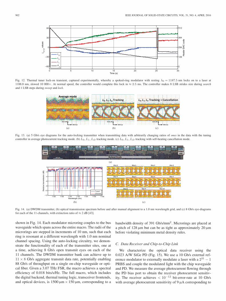
To demonstrate the full capability of the level-tracking cir-cuitry and the self-heating canceller, we change the ratio of
zeros (r0) in the transmitted data. Patterns are randomly gen-erated every 25 ms with different r0, including patterns withr0 = 1 (all zeros) and r0 = 0 (all ones). With the tuner oper-ating in average power lock mode (accomplished by forcingLd = 0, such that L0 = L1 = average of 8192 bits), the mod-ulator eye is completely closed as the controller is unable todiscern changes in r0 from a drift in resonance [Fig. 13(a)].Enabling separate L0, L1, and Ld tracking allows the eye tosettle at the correct value, though each change in r0 causesa sudden change in laser self-heating power, creating tempo-rary eye corruption [Fig. 13(b)]. The self-heating cancellationcircuit compensates for this effect, eliminating the corruption[Fig. 13(b)].
We use the wavelength-locked transmitter components toconstruct a 11-λ DWDM transmitter macro in this platform,
902 IEEE JOURNAL OF SOLID-STATE CIRCUITS, VOL. 51, NO. 4, APRIL 2016
Fig. 12. Thermal tuner lock-on transient, captured experimentally, whereby a spoked-ring modulator with resting λ0 = 1187.5 nm locks on to a laser at1188.8 nm, slowed 10 000×. At normal speed, the controller would complete this lock in ≈ 2.5 ms. The controller makes 8 LSB strides size during searchand 1 LSB steps during sweep and lock.
Fig. 13. (a) 5 Gb/s eye diagrams for the auto-locking transmitter when transmitting data with arbitrarily changing ratios of ones in the data with the tuningcontroller in average photocurrent tracking mode. (b) L0, L1, LD tracking mode. (c) L0, L1, LD tracking with self-heating cancellation mode.
Fig. 14. (a) DWDM transmitter, (b) optical transmission spectrum before and after manual alignment to a 1.0 nm wavelength grid, and (c) 8 Gb/s eye-diagramsfor each of the 11-channels, with extinction ratio of ≈ 2 dB [43].
shown in Fig. 14. Each modulator microring couples to the buswaveguide which spans across the entire macro. The radii of themicrorings are stepped in increments of 10 nm, such that eachring is resonant at a different wavelength with 1.0 nm nominalchannel spacing. Using the auto-locking circuitry, we demon-strate the functionality of each of the transmitter sites, one ata time, achieving 8 Gb/s open transmit eyes on each of the11 channels. The DWDM transmitter bank can achieve up to11× 8 Gb/s aggregate transmit data rate, potentially enabling88 Gb/s of throughput on a single on-chip waveguide or opti-cal fiber. Given a 3.07 THz FSR, the macro achieves a spectralefficiency of 0.018 bits/s/Hz. The full macro, which includesthe digital backend, thermal tuning logic, transceiver frontends,and optical devices, is 1500µm× 150µm, corresponding to a
bandwidth density of 391 Gb/s/mm2. Microrings are placed ata pitch of 128µm but can be as tight as approximately 20µmbefore violating minimum metal density rules.
C. Data Receiver and Chip-to-Chip Link
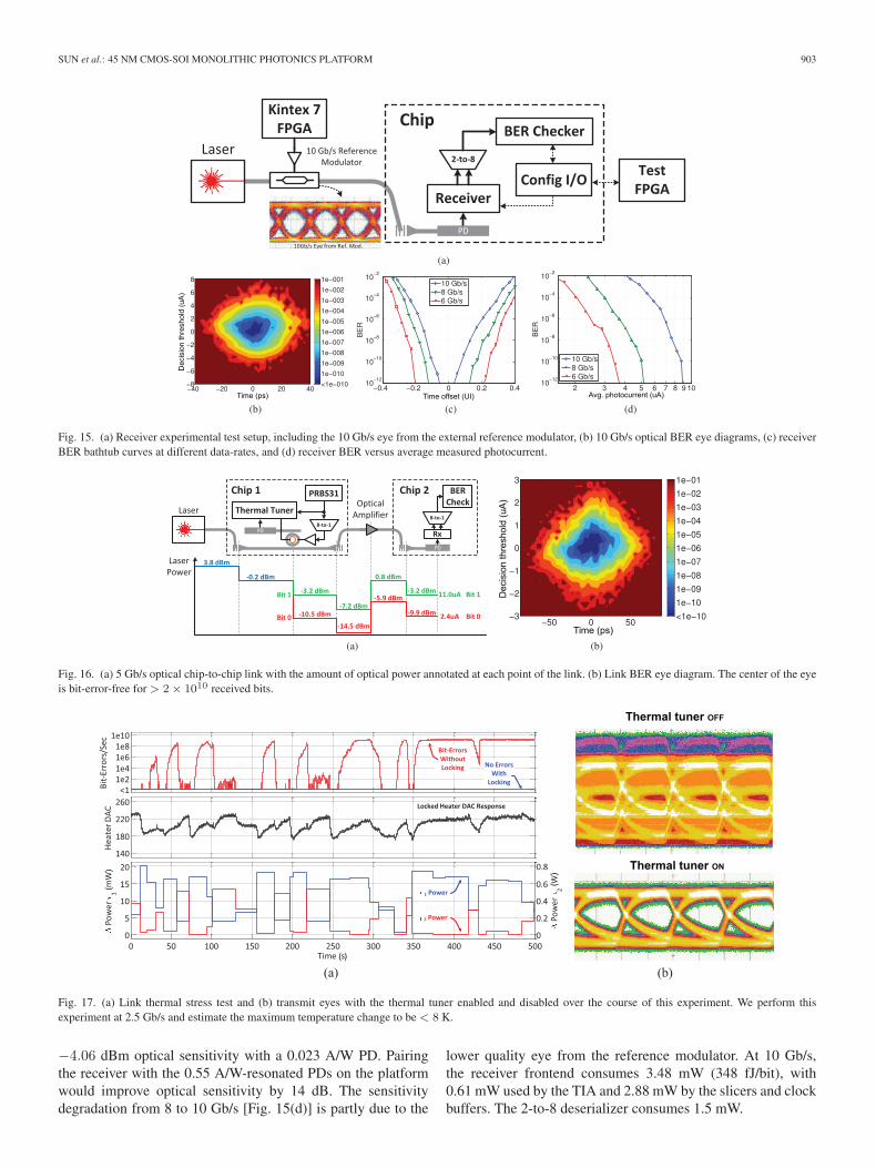
We characterize the optical data receiver using the0.023 A/W SiGe PD (Fig. 15). We use a 10 Gb/s external ref-erence modulator to externally modulate a laser with a 231 − 1PRBS and couple the modulated light with the chip waveguideand PD. We measure the average photocurrent flowing throughthe PD bias port to obtain the receiver photocurrent sensitiv-ity. The receiver achieves < 10−12 bit-error-rate at 10 Gb/swith average photocurrent sensitivity of 9µA corresponding to
SUN et al.: 45 NM CMOS-SOI MONOLITHIC PHOTONICS PLATFORM 903
Fig. 15. (a) Receiver experimental test setup, including the 10 Gb/s eye from the external reference modulator, (b) 10 Gb/s optical BER eye diagrams, (c) receiverBER bathtub curves at different data-rates, and (d) receiver BER versus average measured photocurrent.
Fig. 16. (a) 5 Gb/s optical chip-to-chip link with the amount of optical power annotated at each point of the link. (b) Link BER eye diagram. The center of the eyeis bit-error-free for > 2× 10¹⁰ received bits.
Fig. 17. (a) Link thermal stress test and (b) transmit eyes with the thermal tuner enabled and disabled over the course of this experiment. We perform thisexperiment at 2.5 Gb/s and estimate the maximum temperature change to be < 8 K.
−4.06 dBm optical sensitivity with a 0.023 A/W PD. Pairingthe receiver with the 0.55 A/W-resonated PDs on the platformwould improve optical sensitivity by 14 dB. The sensitivitydegradation from 8 to 10 Gb/s [Fig. 15(d)] is partly due to the
lower quality eye from the reference modulator. At 10 Gb/s,the receiver frontend consumes 3.48 mW (348 fJ/bit), with0.61 mW used by the TIA and 2.88 mW by the slicers and clockbuffers. The 2-to-8 deserializer consumes 1.5 mW.
904 IEEE JOURNAL OF SOLID-STATE CIRCUITS, VOL. 51, NO. 4, APRIL 2016
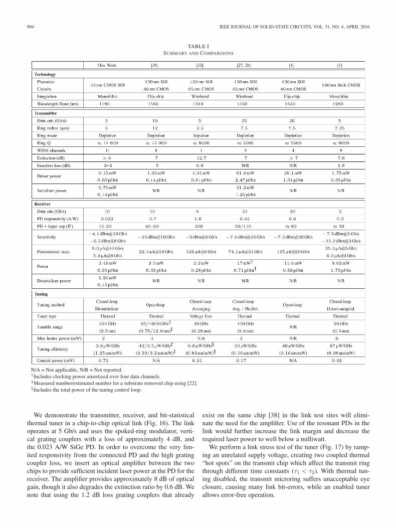
TABLE ISUMMARY AND COMPARISONS
N/A = Not applicable, N/R = Not reported.†Includes clocking power amortized over four data channels.‡Measured number/estimated number for a substrate removed chip using [22].§Includes the total power of the tuning control loop.
We demonstrate the transmitter, receiver, and bit-statisticalthermal tuner in a chip-to-chip optical link (Fig. 16). The linkoperates at 5 Gb/s and uses the spoked-ring modulator, verti-cal grating couplers with a loss of approximately 4 dB, andthe 0.023 A/W SiGe PD. In order to overcome the very lim-ited responsivity from the connected PD and the high gratingcoupler loss, we insert an optical amplifier between the twochips to provide sufficient incident laser power at the PD for thereceiver. The amplifier provides approximately 8 dB of opticalgain, though it also degrades the extinction ratio by 0.6 dB. Wenote that using the 1.2 dB loss grating couplers that already
exist on the same chip [38] in the link test sites will elimi-nate the need for the amplifier. Use of the resonant PDs in thelink would further increase the link margin and decrease therequired laser power to well below a milliwatt.
We perform a link stress test of the tuner (Fig. 17) by ramp-ing an unrelated supply voltage, creating two coupled thermal“hot spots” on the transmit chip which affect the transmit ringthrough different time constants (τ1 < τ2). With thermal tun-ing disabled, the transmit microring suffers unacceptable eyeclosure, causing many link bit-errors, while an enabled tunerallows error-free operation.
SUN et al.: 45 NM CMOS-SOI MONOLITHIC PHOTONICS PLATFORM 905
VI. COMPARISON
We summarize the performance of the platform and com-pare against other works in Table I. The transmitter comparesfavorably in energy efficiency. This is helped, in part, by thelow 1.2 Vpp swing requirement of the modulator device. Amask revision with the proper p-contact implant should improvespeed beyond 5 Gb/s. Compared to other works, the receivercircuit demonstrates a superior 9µA photocurrent sensitiv-ity at 10 Gb/s, benefiting tremendously from its low inputcapacitance. This allows the receiver to achieve comparableoptical sensitivity, despite the crippling 0.023 A/W responsiv-ity of the connected PD. We expect the optical sensitivity toimprove significantly using the 0.55 A/W-resonant PD avail-able in the platform [37], to substitute in on the next chiprevision.
Aided by the thermal isolation of the substrate removed chip,this work achieves the highest measured tuning range and tun-ing efficiency of any on-chip closed-loop tuner reported to date.The extra fidelity provided by the bit-statistical tuner has amodest control power overhead, which could further improvewith properly set timing constraints. Interestingly, of all chip-driven tuners shown here, only this work and [39] (if substrateremoved) have sufficient tuning range to cover the WDMchannel spacing, which is a requirement for dynamic ring-to-channel assignment permutations for reducing tuning costs andachieving virtually unlimited temperature range tolerance [40],[41]. If not satisfied, the thermal tuner must compensate for theentire range of temperature changes, a situation where a temper-ature delta of just 10 K would exceed the tunable range of [4],[27], [28], [33] (and [39] if without substrate removal). Theseresults highlight the importance of providing proper thermalisolation for silicon microring-based photonics.
VII. CONCLUSION
In order for silicon-photonics to be adopted as a next-generation interconnect technology, we must demonstrateelectronic–photonic integration and robust DWDM. The ringresonator is the key device toward achieving these goals, butfaces a number of challenges due to its sensitivity to process,laser power, and temperature variations. This work investi-gated the thermal properties of microring resonators, includingself-heating. To overcome these challenges, we proposed a bit-statistical microring thermal tuner, which can handle arbitrarydata sequences, enable an “eye-max” optimal controller design,and provide self-heating cancellation. The proposed tuner is acritical building block of a “zero-change” electronic–photonicplatform in a commercial 45 nm CMOS-SOI process, enablinga 11 λ DWDM transmitter and a thermally-resilient chip-to-chip optical link. Together with substrate removal and othercomponents on the platform, this work is a key enabler of robustDWDM operation in VLSI electronic–photonic systems [42].
ACKNOWLEDGMENT
The authors gratefully acknowledge the help and supportfrom all POEM team members at MIT, CU Boulder, and UC
Berkeley. The views expressed are those of the authors and donot reflect the official policy or position of the DoD or the U.S.Government.
REFERENCES
[1] I. Young et al., “Optical I/O technology for tera-scale computing,” IEEEJ. Solid-State Circuits, vol. 45, no. 1, pp. 235–248, Jan. 2010.
[2] J. Buckwalter, X. Zheng, G. Li, K. Raj, and A. Krishnamoorthy,“A monolithic 25-Gb/s transceiver with photonic ring modulators and Gedetectors in a 130-nm CMOS SOI process,” IEEE J. Solid-State Circuits,vol. 47, no. 6, pp. 1309–1322, Jun. 2012.
[3] S. Assefa et al., “A 90 nm CMOS integrated nano-photonics technologyfor 25 Gbps WDM optical communications applications,” in Proc. IEEEInt. Electron Devices Meeting (IEDM), Dec. 2012, pp. 33.8.1–33.8.3.
[4] C. Sun et al., “A monolithically-integrated chip-to-chip optical link inbulk CMOS,” IEEE J. Solid-State Circuits, vol. 50, no. 4, pp. 828–844,Apr. 2015.
[5] K. T. Settaluri et al., “Demonstration of an optical chip-to-chip link ina 3D integrated electronic-photonic platform,” in Proc. 41st Eur. Solid-State Circuits Conf. (ESSCIRC), Sep. 2015, pp. 156–159.
[6] E. Timurdogan et al., “An ultra low power 3D integrated intra-chip sili-con electronic-photonic link,” in Proc. Opt. Fiber Commun. Conf., 2015,p. Th5B-8.
[7] I. Shubin et al., “All solid-state multi-chip multi-channel WDM photonicmodule,” in Proc. IEEE 65th Electron. Compon. Technol. Conf. (ECTC),2015, pp. 1293–1298.
[8] M. Rakowski et al., “A 4× 20 Gb/s WDM ring-based hybrid CMOS sil-icon photonics transceiver,” in Proc. IEEE Int. Solid-State Circuits Conf.(ISSCC), 2015, pp. 1–3.
[9] S. Beamer et al., “Re-architecting DRAM memory systems with mono-lithically integrated silicon photonics,” in Proc. Int. Symp. Comput.Archit., 2010, pp. 129–140.
[10] A. N. Udipi, N. Muralimanohar, R. Balasubramonian, A. Davis, andN. P. Jouppi, “Combining memory and a controller with photonicsthrough 3D-stacking to enable scalable and energy-efficient systems,”ACM SIGARCH Comput. Architect. News, vol. 39, no. 3, pp. 425–436,2011.
[11] N. Binkert et al., “The role of optics in future high radix switchdesign,” in Proc. 38th Annu. Int. Symp. Comput. Archit. (ISCA’11), 2011,pp. 437–448.
[12] D. Vantrease et al., “Corona: System implications of emerging nanopho-tonic technology,” in Proc. 35th Annu. Int. Symp. Comput. Architect.(ISCA’08), 2008, pp. 153–164.
[13] A. Joshi et al., “Silicon-photonic clos networks for global on-chip com-munication,” in Proc. 3rd ACM/IEEE Int. Symp. Netw. Chip (NOCS’09),2009, pp. 124–133.
[14] R. A. Soref and B. Bennett, “Electrooptical effects in silicon,” IEEE J.Quantum Electron., vol. QE-23, no. 1, pp. 123–129, Jan. 1987.
[15] Q. Xu, B. Schmidt, S. Pradhan, and M. Lipson, “Micrometre-scale siliconelectro-optic modulator,” Nature, vol. 435, no. 7040, pp. 325–327, 2005.
[16] M. Georgas, J. Orcutt, R. Ram, and V. Stojanovic, “A monolithically-integrated optical receiver in standard 45-nm SOI,” IEEE J. Solid-StateCircuits, vol. 47, no. 7, pp. 1693–1702, Jul. 2012.
[17] S. K. Selvaraja, W. Bogaerts, P. Dumon, D. Van Thourhout, and R. Baets,“Subnanometer linewidth uniformity in silicon nanophotonic waveg-uide devices using CMOS fabrication technology,” IEEE J. Sel. TopicsQuantum Electron., vol. 16, no. 1, pp. 316–324, Jan./Feb. 2010.
[18] M. S. Nawrocka, T. Liu, X. Wang, and R. R. Panepucci, “Tunable sili-con microring resonator with wide free spectral range,” Appl. Phys. Lett.,vol. 89, no. 7, p. 071110, 2006.
[19] P. Dong et al., “Wavelength-tunable silicon microring modulator,” Opt.Express, vol. 18, no. 11, pp. 10941–10946, 2010.
[20] J. S. Orcutt et al., “Nanophotonic integration in state-of-the-art CMOSfoundries,” Opt. Express, vol. 19, no. 3, pp. 2335–2346, Jan. 2011.
[21] G. Li et al., “25 Gb/s 1V-driving CMOS ring modulator with integratedthermal tuning,” Opt. Express, vol. 19, no. 21, pp. 20435–20443, Oct.2011.
[22] P. Dong et al., “Thermally tunable silicon racetrack resonators withultralow tuning power,” Opt. Express, vol. 18, no. 19, pp. 20298–20304,Sep. 2010.
[23] J. S. Orcutt et al., “Open foundry platform for high-performanceelectronic-photonic integration,” Opt. Express, vol. 20, no. 11, pp. 12222–12232, May 2012.
906 IEEE JOURNAL OF SOLID-STATE CIRCUITS, VOL. 51, NO. 4, APRIL 2016
[24] X. Zheng et al., “Enhanced optical bistability from self-heating due tofree carrier absorption in substrate removed silicon ring modulators,” Opt.Express, vol. 20, no. 10, pp. 11478–11486, 2012.
[25] K. Padmaraju, J. Chan, L. Chen, M. Lipson, and K. Bergman, “Thermalstabilization of a microring modulator using feedback control,” Opt.Express, vol. 20, no. 27, pp. 27999–28008, Dec. 2012.
[26] M. T. Wade et al., “Energy-efficient active photonics in a zero-change,state-of-the-art CMOS process,” in Proc. Opt. Fiber Commun. Conf.,2014, p. Tu2E.7.
[27] K. Yu et al., “A 24 Gb/s 0.71 pJ/b Si-photonic source-synchronousreceiver with adaptive equalization and microring wavelength stabiliza-tion,” in Proc. IEEE Int. Solid-State Circuits Conf. (ISSCC), 2015,pp. 1–3.
[28] H. Li et al., “A 25 Gb/s 4.4 V-swing AC-coupled Si-photonic microringtransmitter with 2-tap asymmetric FFE and dynamic thermal tuning in65 nm CMOS,” in Proc. IEEE Int. Solid-State Circuits Conf. (ISSCC),2015, pp. 1–3.
[29] C. Holzwarth et al., “Localized substrate removal technique enablingstrong-confinement microphotonics in bulk Si CMOS processes,”in Proc. Conf. Lasers Electro-Opt./Quantum Electron. Laser Sci.(CLEO/QELS), May 2008, pp. 1–2.
[30] G. Priem, P. Dumon, W. Bogaerts, D. Van Thourhout, G. Morthier,and R. Baets, “Optical bistability and pulsating behaviour in silicon-on-insulator ring resonator structures,” Opt. Express, vol. 13, no. 23,pp. 9623–9628, 2005.
[31] Q. Xu and M. Lipson, “Carrier-induced optical bistability in silicon ringresonators,” Opt. Lett., vol. 31, no. 3, pp. 341–343, 2006.
[32] P. Amberg et al., “A sub-400 fj/bit thermal tuner for optical resonant ringmodulators in 40 nm CMOS,” in Proc. IEEE Asian Solid State CircuitsConf. (A-SSCC), Nov. 2012, pp. 29–32.
[33] C. Li et al., “Silicon photonic transceiver circuits with microring res-onator bias-based wavelength stabilization in 65 nm CMOS,” IEEE J.Solid-State Circuits, vol. 49, no. 6, pp. 1419–1436, Jun. 2014.
[34] W. A. Zortman, A. L. Lentine, D. C. Trotter, and M. R. Watts, “Bit-error-rate monitoring for active wavelength control of resonant modulators,”IEEE Micro, vol. 33, no. 1, pp. 42–52, Jan./Feb. 2013.
[35] J. M. Shainline et al., “Depletion-mode carrier-plasma optical modulatorin zero-change advanced CMOS,” Opt. Lett., vol. 38, no. 15, pp. 2657–2659, 2013.
[36] L. Alloatti, S. Srinivasan, J. Orcutt, and R. Ram, “Waveguide-coupleddetector in zero-change complementary metal-oxide-semiconductor,”Appl. Phys. Lett., vol. 107, no. 4, p. 041104, 2015.
[37] L. Alloatti and R. J. Ram, “Resonance-enhanced waveguide-coupledsilicon-germanium detector,” arXiv preprint, arXiv:1601.00542, 2016
[38] M. Wade et al., “75% efficient wide bandwidth grating couplers in a45 nm microelectronics CMOS process,” in Proc. Opt. InterconnectsConf., Apr. 2015, pp. 46–47.
[39] F. Y. Liu et al., “10-Gbps, 5.3-mW optical transmitter and receiver circuitsin 40-nm CMOS,” IEEE J. Solid-State Circuits, vol. 47, no. 9, pp. 2049–2067, Sep. 2012.
[40] A. V. Krishnamoorthy et al., “Exploiting CMOS manufacturing to reducetuning requirements for resonant optical devices,” IEEE Photonics J.,vol. 3, no. 3, pp. 567–579, Jun. 2011.
[41] M. Georgas, J. Leu, B. Moss, C. Sun, and V. Stojanovic, “Addressinglink-level design tradeoffs for integrated photonic interconnects,” in Proc.IEEE Custom Integr. Circuits Conf. (CICC), Sep. 2011, pp. 1–8.
[42] C. Sun et al., “Single-chip microprocessor that communicates directlyusing light,” Nature, vol. 528, no. 7583, pp. 534–538, 2015.
[43] C. Sun et al., “A 45 nm SOI monolithic photonics chip-to-chip link withbit-statistics-based resonant microring thermal tuning,” in Symp. VLSICircuits Dig. Tech. Papers, Jun. 2015, pp. C122–C123.
Chen Sun (M’16) received the B.S. degree in elec-trical engineering and computer science from theUniversity of California, Berkeley, CA, USA, in2009, and the S.M. and Ph.D. degrees in electri-cal engineering from the Massachusetts Institute ofTechnology, Cambridge, MA, USA, in 2011 and2015, respectively.
Since 2013, he has been a Visiting StudentResearcher at Berkeley Wireless Research Center,University of California, Berkeley. He was thecofounder of Ayar Labs, Inc., Cambridge, MA, USA,
in 2015. Previously, he held internships with Nvidia, Santa Clara, CA, USA,and Rambus, Sunnyvale, CA, USA. His research interests include the design ofenergy-efficient interconnects, modeling and implementation of electro-opticdevices and systems, and techniques for DWDM optical transceivers.
Mark Wade received the B.S. degrees in electri-cal engineering and physics from Louisiana TechUniversity, Ruston, LA, USA, in 2010, and the M.S.and Ph.D. degrees in electrical engineering from theUniversity of Colorado, Boulder, CO, USA, in 2013and 2015, respectively.
He was the cofounder of Ayar Labs, Inc.,Cambridge, MA, USA, in 2015. His research interestsinclude integrated photonic devices for electronic–photonic WDM communication systems.
Dr. Wade was a NIST Measurement, Science, andEngineering Fellow and a National Science Foundation Graduate ResearchFellow.
Michael Georgas received the B.A.Sc. degree inengineering science from the University of Toronto,Toronto, ON, Canada, in 2007, the Master’s degreefrom the Massachusetts Institute of Technology(MIT), Cambridge, MA, USA, in 2009, and the Ph.D.degree in electrical engineering and computer sciencefrom MIT in 2013.
He is a Postdoctoral Associate with the ResearchLaboratory of Electronics Translational FellowsProgram, MIT. His research interests include inte-grated photonics and high-speed links, and more
recently the application and commercialization of integrated photonics indata-centers.
Sen Lin received the B.S. degree in microelectron-ics from Tsinghua University, Beijing, China, in2012. He is currently pursuing the Ph.D. degree inProf. Vladimir Stojanovic’s group at the Universityof California, Berkeley, CA, USA. He is a memberof Berkeley Wireless Research Center. His researchinterests include design and modeling of silicon pho-tonic systems and high-speed communication links.He held an internship with Xilinx, San Jose, CA,USA, in 2015.
Luca Alloatti received the M.Sc. degree in physicsfrom the University of Pisa, Pisa, Italy, in 2004,the “Diploma di Licenza” from Scuola NormaleSuperiore di Pisa, Pisa, Italy, in 2006, and thePh.D. degree in electrical engineering from KarlsruheInstitute of Technology (KIT), Karlsruhe, Germany,with a thesis entitled “High-Speed, Low-Power andMid-IR Silicon Photonics Applications,” in 2012.
In December 2013, he joined the MassachusettsInstitute of Technology, Cambridge, MA, USA,where he demonstrated “zero-change CMOS” high-
speed detectors and modulators as well as a photonic design automation(PDA) infrastructure based on Cadence. Since December 2015, he has beena Research Scientist with ETH-Zurich, Switzerland.
Benjamin Moss received the B.S. degree from theMissouri University of Science and Technology,Rolla, MO, USA, in 2006, the M.S. degree inelectrical engineering and computer science fromthe Massachusetts Institute of Technology (MIT),Cambridge, MA, USA, in 2009, and the Ph.D. degreein electrical engineering and computer science fromMIT.
His research interests include applications of high-speed photonic interconnects in industry applications.
SUN et al.: 45 NM CMOS-SOI MONOLITHIC PHOTONICS PLATFORM 907
Rajesh Kumar was born in India, in 1984. Hereceived the M.Tech. degree in optoelectronics andoptical communication from the Indian Institute ofTechnology (IIT) Delhi, New Delhi, India, in 2008,and the Ph.D. degree in photonics engineering fromIMEC, Ghent University, Ghent, Belgium, in 2012.
He investigated InP-on-SOI microdisks for var-ious optical signal processing applications whileworking with IMEC, Ghent University. After com-pleting the Ph.D. degree, he worked with theOptoelectronics Research Center, University of
Southampton, Southampton, U.K., from 2012 to 2013, and with the Universityof Colorado, Boulder, CO, USA, from 2013 to 2015. He has authored or coau-thored more than 40 peer-reviewed papers in different journals and conferenceproceedings. His research interests include optical interconnects, optical logicand optical signal processing.
Dr. Kumar is a member of OSA and serves as a Reviewer for various opticsand photonics journals.
Amir H. Atabaki received the B.S. and M.S. degreesin electrical engineering from Sharif University ofTechnology, Tehran, Iran, in 2003 and 2005, respec-tively, and the Ph.D. degree in electrical and computerengineering from Georgia Institute of Technology,Atlanta, GA, USA, in 2011.
Currently, he is a Senior Postdoctoral Associatewith the Research Laboratory of Electronics,Massachusetts Institute of Technology, Cambridge,MA, USA. His research interests include photonicdevice and material development in CMOS plat-
forms for applications in optical interconnects, spectroscopy, imaging, andRF-photonics.
Fabio Pavanello received the M.Sc. degree in phys-ical engineering from the Polytechnic University ofTurin, Turin, Italy in 2010, and the Ph.D. degree inelectrical engineering from the University of Lille I,Lille, France, in 2013.
During the Ph.D. degree, he worked on the devel-opment of high-speed photodiodes based on III-Vmaterials as efficient THz sources. Since 2014, hehas been working as a Research Associate withthe University of Colorado, Boulder, CO, USA. Hisresearch interests include the development of a wide
range of photonic devices in advanced CMOS platforms for monolithicelectronics–photonics integration.
Jeffrey M. Shainline received the B.S. degree inphysics from the University of Colorado Boulder,Boulder, CO, USA, in 2005, and the Ph.D. degreefrom Brown University, Providence, RI, USA, in2010.
From 2010 to 2013, he was a PostdoctoralResearcher with the Laboratory of Dr. Milos Popovic,University of Colorado Boulder, Boulder, CO, USA.In 2013, he joined the Division of Optoelectronicsand Photonics, National Institute of Standards andTechnology, Boulder, CO, USA, as a National
Research Council Postdoctoral Fellow. His research interests include theintegration of chip-scale quantum photonic devices with superconductingsingle-photon detectors.
Jason S. Orcutt received the B.S. degree in elec-trical engineering from Columbia University, NewYork, NY, USA, in 2005, and the M.S. and Ph.D.degrees in electrical engineering and computer sci-ence from the Massachusetts Institute of Technology(MIT), Cambridge, MA, USA, in 2008 and 2012,respectively.
From 2012 to 2013, he worked as a ResearchScientist with MIT. Since 2013, he has been aResearch Staff Member with the Department ofPhysical Sciences, IBM T. J. Watson Research
Center, Yorktown Heights, NY, USA. His research interests include ultrafastand integrated optics to bioelectronics and stochastic systems.
Dr. Orcutt was the recipient of the National Sciences Foundation GraduateResearch Fellowship from 2005 to 2008.
Rajeev J. Ram (F’16) received the B.S. degreein applied physics from the California Institute ofTechnology, Pasadena, CA, USA, in 1991, and thePh.D. degree in electrical engineering from theUniversity of California, Santa Barbara, CA, USA, in1997.
He is currently a Professor with the MassachusettsInstitute of Technology, Cambridge, MA, USA. Hisresearch interests include physical optics and elec-tronics, the development of novel components andsystems for communications and sensing, and studies
of fundamental interactions between electronic materials and light.
Miloš Popovic (M’05) was born in Zajear, Serbia,formerly Yugoslavia, in 1977. He received theB.Sc.E. degree in electrical engineering fromQueen’s University, Kingston, ON, Canada, in 1999,and the M.S. and Ph.D. degrees in electrical engineer-ing from the Massachusetts Institute of Technology,Cambridge, MA, USA, in 2002 and 2008, respec-tively.
Since 2010, he has been an Assistant Professorwith the Department of Electrical, Computer,and Energy Engineering, University of Colorado,
Boulder, CO, USA. In 2012, he was named a Fellow of the David and LucilePackard Foundation. He is the inventor or co-inventor on over 16 patents, andthe author or coauthor of over 130 research papers and two book chapters. Hisresearch interests include silicon photonic circuits, CMOS photonics integra-tion and optical interconnects, nonlinear and quantum integrated photonics,light-forces-based nanomechanical photonic devices, the application of elec-tromagnetic theory, and solid-state physics toward the invention of devices thatfunction based on novel aspects of the physics of light-matter interaction. Heis also interested in electromagnetic theory and numerical methods related tophotonics.
Dr. Popovic has served on the Technical Program Committees for theOptical Fiber Communication Conference (OFC), the Conference on Lasersand Electro-Optics (CLEO), Integrated Photonics Research (IPR), and GroupIV Photonics (GFP).
Vladimir Stojanovic (M’04) received the Dipl.Ing.degree from the University of Belgrade, Belgrade,Serbia, in 1998, and the Ph.D. degree in electricalengineering from Stanford University, Stanford, CA,USA, in 2005.
He is an Associate Professor of ElectricalEngineering and Computer Science with theUniversity of California, Berkeley, CA, USA. Hewas also with Rambus, Inc., Los Altos, CA, USA,as a Principal Engineer from 2001 through 2004and with the Massachusetts Institute of Technology,
Cambridge, MA, USA, as an Associate Professor from 2005 to 2013. Hisresearch interests include design, modeling, and optimization of integratedsystems, from CMOS-based VLSI blocks and interfaces to system design withemerging devices like NEM relays and silicon-photonics. He is also interestedin design and implementation of energy-efficient electrical and opticalnetworks, and digital communication techniques in high-speed interfaces andhigh-speed mixed-signal IC design.
Dr. Stojanovic was an IEEE Solid-State Circuits Society DistinguishedLecturer for the 2012–2013 term. He was the recipient of the 2006 IBM FacultyPartnership Award, and the 2009 NSF CAREER Award as well as the 2008ICCAD William J. McCalla, 2008 IEEE Transactions on Advanced Packaging,and 2010 ISSCC Jack Raper Best Paper Awards.