a 30 gb/s cmos driver integrated with silicon photonics mzm · a 30 gb/s cmos driver integrated...
TRANSCRIPT
A 30 Gb/s CMOS driver integrated with silicon photonics MZM
Ke Li , Dave J.Thomson, Shenghao Liu, Peter Wilson, and Graham. T. Reed Silicon Photonics Group, Zepler Institute, University of Southampton
Abstract— A voltage mode modulator driver is proposed
in the TSMC 65nm low power CMOS process. In the electrical testing, the driver itself can achieve a bit rate of 40Gb/s with the single-ended output swing of 1.65V. Unlike equivalent CML modulator drivers, when the proposed driver is integrated with the silicon photonic MZM, it does not require an additional biasing network. The integrated electro-optic transmitter can achieve 30Gb/s with an extinction ratio of 4.05dB, with the power consumption of main driver being 323mW.
Index Terms—modulator driver, silicon photonics, Mach-Zehnder Modulator (MZM), power amplifiers.
I. INTRODUCTION As data traffic continually increases, the demand on
the network infrastructure is becoming increasingly strained. Electronic interconnects over short reaches, such as board to board or chip to chip, are struggling to keep up with bandwidth and/or power consumption requirements. One solution is to migrate from copper to optical based interconnects since data can be sent in an optical format over very long distances with minimal loss and lower power consumption. Silicon photonics is excellently placed to match the performance and cost requirements of these short reach applications [1][4]. Silicon photonics takes advantage of the fact that components can be formed using CMOS like processes in CMOS fabrication facilities and therefore photonic integrated circuits based in silicon, as such, SiP circuits can be produced with high accuracy and yield at much lower cost than components based in more traditional photonic materials such as LiNbO3 or III-V compounds.
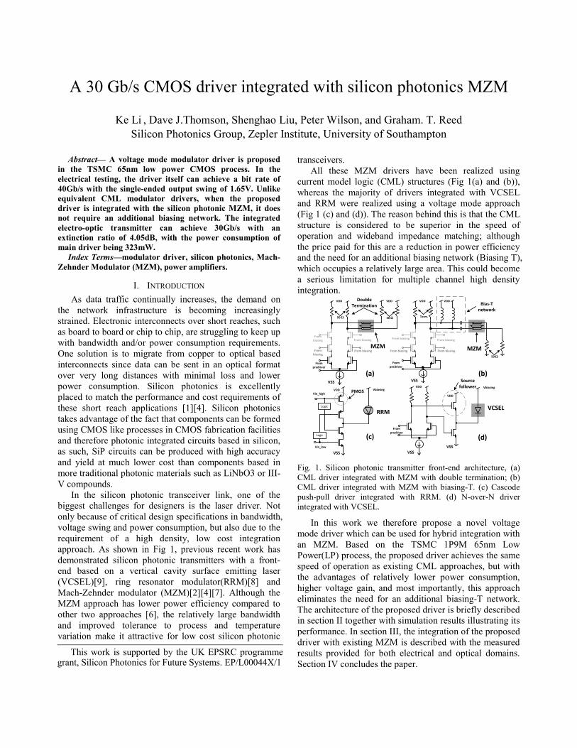
In the silicon photonic transceiver link, one of the biggest challenges for designers is the laser driver. Not only because of critical design specifications in bandwidth, voltage swing and power consumption, but also due to the requirement of a high density, low cost integration approach. As shown in Fig 1, previous recent work has demonstrated silicon photonic transmitters with a front-end based on a vertical cavity surface emitting laser (VCSEL)[9], ring resonator modulator(RRM)[8] and Mach-Zehnder modulator (MZM)[2][4][7]. Although the MZM approach has lower power efficiency compared to other two approaches [6], the relatively large bandwidth and improved tolerance to process and temperature variation make it attractive for low cost silicon photonic
transceivers. All these MZM drivers have been realized using
current model logic (CML) structures (Fig 1(a) and (b)), whereas the majority of drivers integrated with VCSEL and RRM were realized using a voltage mode approach (Fig 1 (c) and (d)). The reason behind this is that the CML structure is considered to be superior in the speed of operation and wideband impedance matching; although the price paid for this are a reduction in power efficiency and the need for an additional biasing network (Biasing T), which occupies a relatively large area. This could become a serious limitation for multiple channel high density integration.
Fig. 1. Silicon photonic transmitter front-end architecture, (a) CML driver integrated with MZM with double termination; (b) CML driver integrated with MZM with biasing-T. (c) Cascode push-pull driver integrated with RRM. (d) N-over-N driver integrated with VCSEL.
In this work we therefore propose a novel voltage mode driver which can be used for hybrid integration with an MZM. Based on the TSMC 1P9M 65nm Low Power(LP) process, the proposed driver achieves the same speed of operation as existing CML approaches, but with the advantages of relatively lower power consumption, higher voltage gain, and most importantly, this approach eliminates the need for an additional biasing-T network. The architecture of the proposed driver is briefly described in section II together with simulation results illustrating its performance. In section III, the integration of the proposed driver with existing MZM is described with the measured results provided for both electrical and optical domains. Section IV concludes the paper.
From biasing
From biasing
From biasing From biasing
From predriver
VSS
VDD
50 Ω
MZM
Double Termination
(a)
VDD
50 Ω
From biasing From biasing
From biasing From biasing
From predriver
VSS
VDD
50 Ω
MZM
(b)
VDDBias-T
networkTerm.
(d)
VCSEL
VDD
VSS
Vbiasing
(c)
RRM
VDD
Vin_low
VSS
VbiasingVin_high
Logic
Logic
From predriver
VSS
VDD
Source follower
PMOS
This work is supported by the UK EPSRC programme grant, Silicon Photonics for Future Systems. EP/L00044X/1
II. PROPOSED DESIGN There are three main challenges in the design of the
modulator driver coupled to the MZM. Firstly, MZM in general require a relatively large voltage swing, which is much higher than the typical CMOS transistor breakdown voltage. Secondly, an adequate switching speed needs to be provided to prevent inter symbol interference (ISI) at the required data rates. Finally, since the MZM uses a 50Ω coplanar transmission line, proper impedance matching mechanisms need to be created to prevent impedance discontinuities.
A. Design concept To face the design challenge of the output voltage
swing, conventionally, a CML approach (Fig 1 (a) and (b)) [2-4][7] uses cascaded transistors to generate a large output swing, provided that double termination or external inductor pull-up network is used. However, as is shown in Fig 1(c) [8], it has been demonstrated that a cascaded push-pull driver can supply a large output swing without using a external biasing network. However, the low speed PMOS transistor in the top of output stage always limits the driver’s speed of operation, and the two independent pre-drivers have to be created at different voltage level for the top and bottom input signals (Vin_high and Vin_low). N-over-N voltage mode drivers can eliminate the using of this low speed PMOS transistor [9], however, as shown in Fig 1(d), the top NMOS transistor naturally operates as a source follower and hence has a voltage gain less than 1, which reduces the output voltage swing.
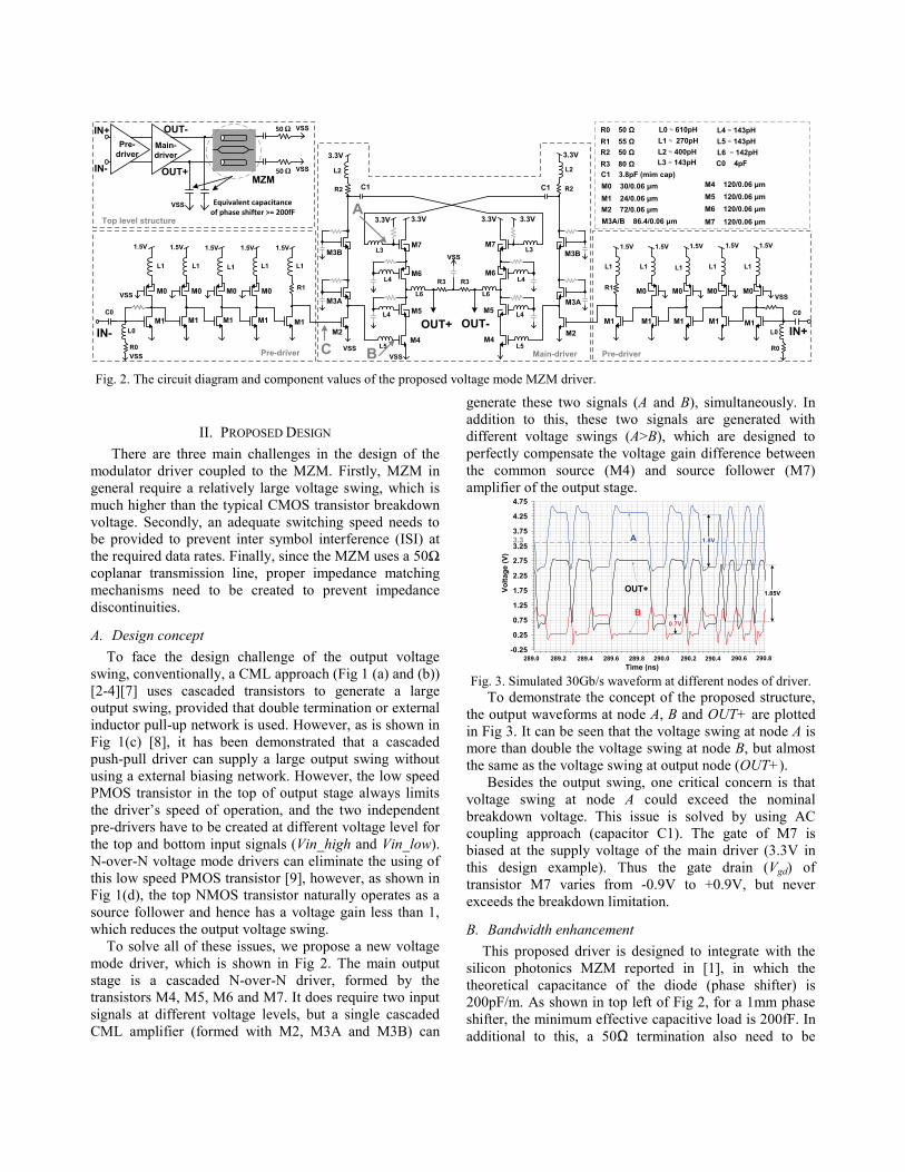
To solve all of these issues, we propose a new voltage mode driver, which is shown in Fig 2. The main output stage is a cascaded N-over-N driver, formed by the transistors M4, M5, M6 and M7. It does require two input signals at different voltage levels, but a single cascaded CML amplifier (formed with M2, M3A and M3B) can
generate these two signals (A and B), simultaneously. In addition to this, these two signals are generated with different voltage swings (A>B), which are designed to perfectly compensate the voltage gain difference between the common source (M4) and source follower (M7) amplifier of the output stage.
Fig. 3. Simulated 30Gb/s waveform at different nodes of driver.
To demonstrate the concept of the proposed structure, the output waveforms at node A, B and OUT+ are plotted in Fig 3. It can be seen that the voltage swing at node A is more than double the voltage swing at node B, but almost the same as the voltage swing at output node (OUT+).
Besides the output swing, one critical concern is that voltage swing at node A could exceed the nominal breakdown voltage. This issue is solved by using AC coupling approach (capacitor C1). The gate of M7 is biased at the supply voltage of the main driver (3.3V in this design example). Thus the gate drain (Vgd) of transistor M7 varies from -0.9V to +0.9V, but never exceeds the breakdown limitation.
B. Bandwidth enhancement This proposed driver is designed to integrate with the
silicon photonics MZM reported in [1], in which the theoretical capacitance of the diode (phase shifter) is 200pF/m. As shown in top left of Fig 2, for a 1mm phase shifter, the minimum effective capacitive load is 200fF. In additional to this, a 50Ω termination also need to be
-0.25
0.25
0.75
1.25
1.75
2.25
2.75
3.25
3.75
4.25
4.75
Time (ns)289.0 289.2 289.4 289.6 289.8 290.0 290.2 290.4 290.6 290.8
Volta
ge (V
)
A
B
OUT+
3.3
1.85V
1.8V
0.7V
1.5V 1.5V 1.5V 1.5V 1.5V 1.5V 1.5V 1.5V 1.5V 1.5V
3.3V 3.3V
3.3V3.3V 3.3V
L1 L1 L1 L1 L1 L1 L1 L1 L1 L1
M1 M1 M1 M1 M1M2
M3A
M3B
M4
M5
M6
M7
M4
M5
M6
M7
M0 M0 M0 M0 M0 M0 M0 M0
M2
M3A
M3B
L2 L2
L3 L3
L4
L4
L5 L5
L4
L4
C1 C1
R1
L0
R0
L0
R0
R1
R2 R2
L6 L6
M1 M1 M1 M1 M1
M1 24/0.06 μm
R3 R3
M0 30/0.06 μm
M2 72/0.06 μm M3A/B 86.4/0.06 μm
M4 120/0.06 μm M5 120/0.06 μm M6 120/0.06 μm M7 120/0.06 μm
C0 C0
C0 4pF C1 3.8pF (mim cap)
OUT+ OUT-IN- IN+
VSSVSSVSS
3.3VA
BPre-driver Pre-driverMain-driverC
VSS
VSSVSS
R0 50 Ω R1 55 Ω R2 50 Ω R3 80 Ω
L1 ≈ 270pH L2 ≈ 400pH L3 ≈ 143pH
L4 ≈ 143pH L5 ≈ 143pH L6 ≈ 142pH
L0 ≈ 610pH
50 Ω
50 Ω IN+
IN- OUT+
OUT-Pre-
driverMain-driver
VSS
VSS
VSS Equivalent capacitance of phase shifter >= 200fF
MZM
Top level structure
Fig. 2. The circuit diagram and component values of the proposed voltage mode MZM driver.
included. To drive these loads with a relatively large output voltage swing, large transistors are required, which leads to a serious impact of parasitic capacitance in the final implemented design (layout).
Fig. 4. Simulated frequency response of the main-driver with
different inductor peaking mechanism. To address this issue, firstly, 5 stages pre-driver were
incorporated within the design to boost the voltage gain of the overall transmitter. Secondly, a variety of inductors were used to create shunt series inductor peaking architectures [7], which can enhance the bandwidth of the main-driver. Fig 4 illustrates the simulated frequency response of the main-driver under different combinations of inductor peaking structure. As can be seen, the 3dB bandwidth can be enhanced from 9GHz to 19.5GHz, and group delay variation can be maintained within 8ps.
In order to minimize the layout area, all the inductors used within this design were full custom designs, analysed with EM analysis tools including ADS. Fig 5 illustrates the analytical results of one of the inductors (L5) used in this design, which occupies an area of 20μm ×30μm.
Fig. 5.Analytical results of On-chip inductor (L5), and its 3-D layout view.
C. Output impedance matching The control of the output impedance for a voltage
mode driver is generally much more difficult than with the CML approach. Previous work [10] proposes additional calibration techniques to control the output impedance. However, at high frequencies, these additional calibration functions at the output node will have the effect of introducing more unnecessary parasitic effects at the output node. Given that the physical length of the 50Ω coplanar transmission line on MZM is in the range of 1-2mm, the requirement for the precise impedance matching can in fact be relaxed.
In the proposed design, a fixed value shunt resistor (R3=80Ω) is used for the termination. The overall output impedance would be parallel combination of the R3,
effective resistance of M6+M7 and M4+M5. This mechanism does not perfectly match to 50Ω, but as shown in Fig 6, simulation results show that it still can provide a low frequency return loss at -25dB.
Fig. 6.Simulated differential return loss of the proposed driver.
III. EXPERIMENTAL RESULTS The proposed design was fabricated in TSMC 65nm
1P9M LP CMOS process. As shown in Fig 8(b), the overall active area is 345μm × 380μm, in which the area of the main driver is 345μm × 210μm.
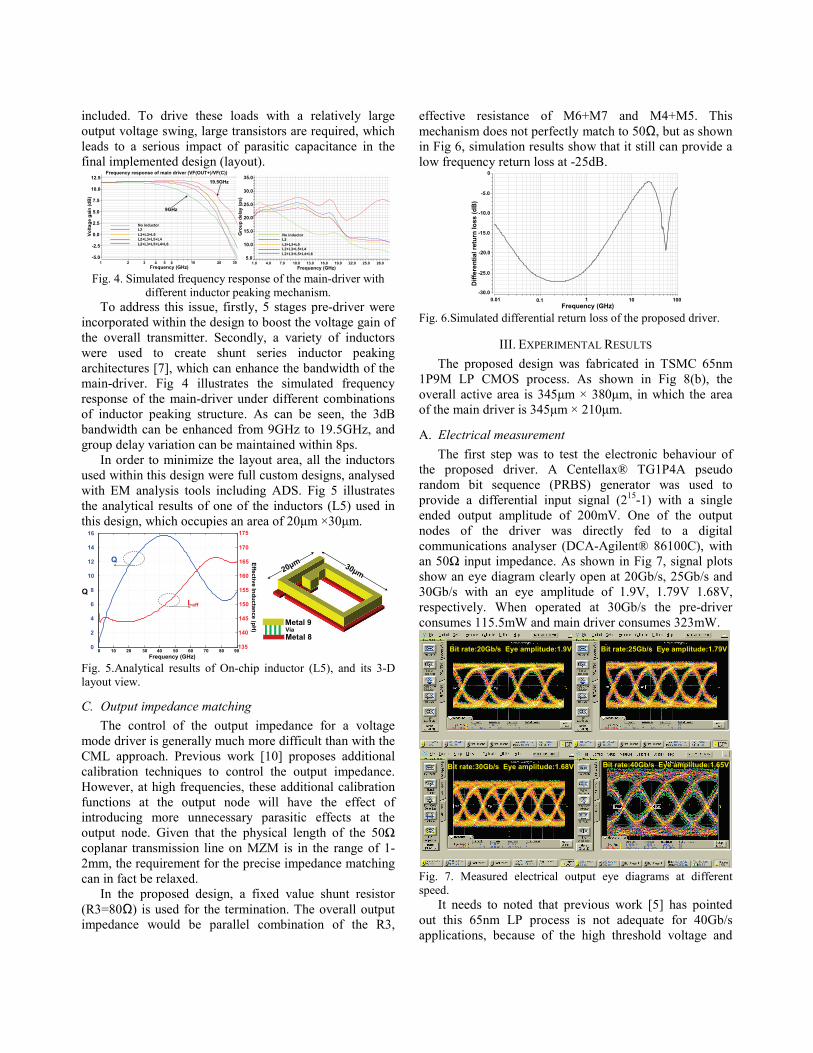
A. Electrical measurement The first step was to test the electronic behaviour of
the proposed driver. A Centellax® TG1P4A pseudo random bit sequence (PRBS) generator was used to provide a differential input signal (215-1) with a single ended output amplitude of 200mV. One of the output nodes of the driver was directly fed to a digital communications analyser (DCA-Agilent® 86100C), with an 50Ω input impedance. As shown in Fig 7, signal plots show an eye diagram clearly open at 20Gb/s, 25Gb/s and 30Gb/s with an eye amplitude of 1.9V, 1.79V 1.68V, respectively. When operated at 30Gb/s the pre-driver consumes 115.5mW and main driver consumes 323mW.
Fig. 7. Measured electrical output eye diagrams at different speed.
It needs to noted that previous work [5] has pointed out this 65nm LP process is not adequate for 40Gb/s applications, because of the high threshold voltage and
Volta
ge g
ain
(dB
)
-5.0
-2.5
0.0
2.5
5.0
7.5
10.0
12.5
Frequency (GHz)1 2 10 20 303 4 5 6
No inductorL2L2+L3+L5L2+L3+L5+L4L2+L3+L5+L4+L6
19.5GHz
5.0
10.0
15.0
20.0
25.0
30.0
35.0
1.0 4.0 7.0 10.0 13.0 16.0 19.0 22.0 25.0 28.0Frequency (GHz)
Gro
up d
elay
(ps)
9GHz
Frequency response of main driver (VF(OUT+)/VF(C))
No inductorL2L2+L3+L5L2+L3+L5+L4L2+L3+L5+L4+L6
0 10 20 30 40 50 60 70 80 900
2
4
6
8
10
12
14
16
135
140
145
150
155
160
165
170
175
Frequency (GHz)
Q
Effective Inductance (pH)
Q
Leff
20μm 30μm
Metal 9
Metal 8Via
Frequency (GHz)0.01 0.1 1 10 100
Diff
eren
tial r
etur
n lo
ss (d
B)
-10.0
-5.0
0
-15.0
-20.0
-25.0
-30.0
Bit rate:20Gb/s Eye amplitude:1.9V Bit rate:25Gb/s Eye amplitude:1.79V
Bit rate:30Gb/s Eye amplitude:1.68V Bit rate:40Gb/s Eye amplitude:1.65V
insufficient ft (<150GHz). As shown in the bottom right of Fig 7, when the supply voltage of main driver is increased to 3.6V, a 40Gb/s eye diagram can be observed with amplitude at 1.65V, with the power consumption of main driver increased to 396mW. This result is consistent with the conclusion in [5].
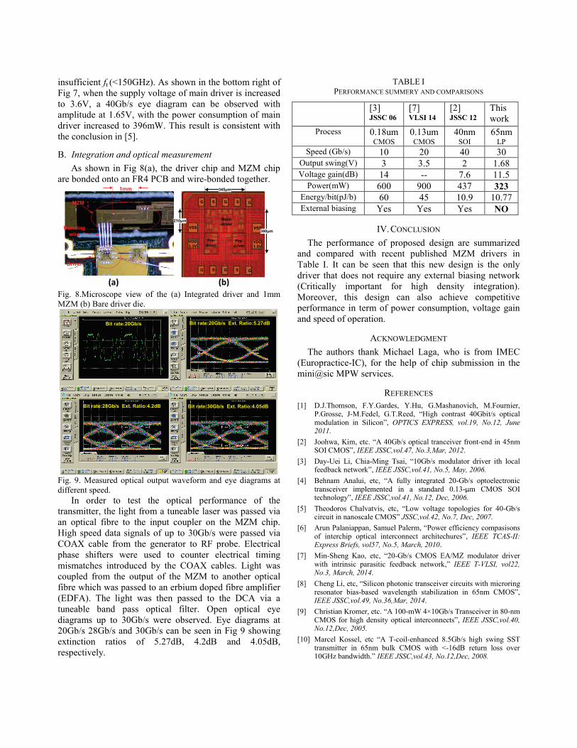
B. Integration and optical measurement As shown in Fig 8(a), the driver chip and MZM chip
are bonded onto an FR4 PCB and wire-bonded together.
Fig. 8.Microscope view of the (a) Integrated driver and 1mm MZM (b) Bare driver die.
Fig. 9. Measured optical output waveform and eye diagrams at different speed.
In order to test the optical performance of the transmitter, the light from a tuneable laser was passed via an optical fibre to the input coupler on the MZM chip. High speed data signals of up to 30Gb/s were passed via COAX cable from the generator to RF probe. Electrical phase shifters were used to counter electrical timing mismatches introduced by the COAX cables. Light was coupled from the output of the MZM to another optical fibre which was passed to an erbium doped fibre amplifier (EDFA). The light was then passed to the DCA via a tuneable band pass optical filter. Open optical eye diagrams up to 30Gb/s were observed. Eye diagrams at 20Gb/s 28Gb/s and 30Gb/s can be seen in Fig 9 showing extinction ratios of 5.27dB, 4.2dB and 4.05dB, respectively.
TABLE I PERFORMANCE SUMMERY AND COMPARISONS
[3] JSSC 06
[7] VLSI 14
[2] JSSC 12
This work
Process 0.18um CMOS
0.13um CMOS
40nm SOI
65nm LP
Speed (Gb/s) 10 20 40 30 Output swing(V) 3 3.5 2 1.68 Voltage gain(dB) 14 -- 7.6 11.5
Power(mW) 600 900 437 323 Energy/bit(pJ/b) 60 45 10.9 10.77 External biasing Yes Yes Yes NO
IV. CONCLUSION The performance of proposed design are summarized
and compared with recent published MZM drivers in Table I. It can be seen that this new design is the only driver that does not require any external biasing network (Critically important for high density integration). Moreover, this design can also achieve competitive performance in term of power consumption, voltage gain and speed of operation.
ACKNOWLEDGMENT The authors thank Michael Laga, who is from IMEC
(Europractice-IC), for the help of chip submission in the mini@sic MPW services.
REFERENCES [1] D.J.Thomson, F.Y.Gardes, Y.Hu, G.Mashanovich, M.Fournier,
P.Grosse, J-M.Fedel, G.T.Reed, “High contrast 40Gbit/s optical modulation in Silicon”, OPTICS EXPRESS, vol.19, No.12, June 2011.
[2] Joohwa, Kim, etc. “A 40Gb/s optical tranceiver front-end in 45nm SOI CMOS”, IEEE JSSC,vol.47, No.3,Mar, 2012.
[3] Day-Uei Li, Chia-Ming Tsai, “10Gb/s modulator driver ith local feedback network”, IEEE JSSC,vol.41, No.5, May, 2006.
[4] Behnam Analui, etc, “A fully integrated 20-Gb/s optoelectronic transceiver implemented in a standard 0.13-µm CMOS SOI technology”, IEEE JSSC,vol.41, No.12, Dec, 2006.
[5] Theodoros Chalvatvis, etc, “Low voltage topologies for 40-Gb/s circuit in nanoscale CMOS” JSSC,vol.42, No.7, Dec, 2007.
[6] Arun Palaniappan, Samuel Palerm, “Power efficiency compasisons of interchip optical interconnect architechures”, IEEE TCAS-II: Express Briefs, vol57, No.5, March, 2010.
[7] Min-Sheng Kao, etc, “20-Gb/s CMOS EA/MZ modulator driver with intrinsic parasitic feedback network,” IEEE T-VLSI, vol22, No.3, March, 2014.
[8] Cheng Li, etc, “Silicon photonic transceiver circuits with microring resonator bias-based wavelength stabilization in 65nm CMOS”, IEEE JSSC,vol.49, No.36,Mar, 2014.
[9] Christian Kromer, etc. “A 100-mW 4×10Gb/s Transceiver in 80-nm CMOS for high density optical interconnects”, IEEE JSSC,vol.40, No.12,Dec, 2005.
[10] Marcel Kossel, etc “A T-coil-enhanced 8.5Gb/s high swing SST transmitter in 65nm bulk CMOS with <-16dB return loss over 10GHz bandwidth.” IEEE JSSC,vol.43, No.12,Dec, 2008.
MZM
Driver
Bonding wire
1mm
VSS VSS
VDD3.3V
VDD1.5V
G S G S G
G S G S G
380μm
345μm
Pre-driver
Main-driver
210μm
Pre-driver
(a) (b)
Bit rate:20Gb/s Ext. Ratio:5.27dB
Bit rate:30Gb/s Ext. Ratio:4.05dBBit rate:28Gb/s Ext. Ratio:4.2dB
Bit rate:20Gb/s