93xx86 varias versiones
TRANSCRIPT
93AA86A/B/C, 93LC86A/B/C,93C86A/B/C
16K Microwire Compatible Serial EEPROM
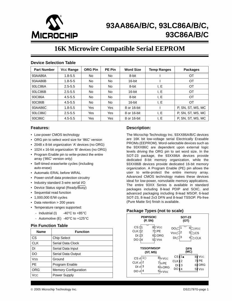
Device Selection Table
Features:
• Low-power CMOS technology
• ORG pin to select word size for ‘86C’ version• 2048 x 8-bit organization ‘A’ devices (no ORG)• 1024 x 16-bit organization ‘B’ devices (no ORG)
• Program Enable pin to write-protect the entire array (‘86C’ version only)
• Self-timed erase/write cycles (including auto-erase)
• Automatic ERAL before WRAL• Power-on/off data protection circuitry• Industry standard 3-wire serial I/O
• Device Status signal (Ready/Busy)• Sequential read function• 1,000,000 E/W cycles
• Data retention > 200 years• Temperature ranges supported:
Pin Function Table
Description:
The Microchip Technology Inc. 93XX86A/B/C devicesare 16K bit low-voltage serial Electrically ErasablePROMs (EEPROM). Word-selectable devices such asthe 93XX86C are dependent upon external logiclevels driving the ORG pin to set word size. In theSOT-23 package, the 93XX86A devices providededicated 8-bit memory organization, while the93XX86B devices provide dedicated 16-bit memoryorganization. A Program Enable (PE) pin allows theuser to write-protect the entire memory array.Advanced CMOS technology makes these devicesideal for low-power, nonvolatile memory applications.The entire 93XX Series is available in standardpackages including 8-lead PDIP and SOIC, andadvanced packaging including 8-lead MSOP, 6-leadSOT-23, 8-lead 2x3 DFN and 8-lead TSSOP. Pb-free(Pure Matte Sn) finish is available.
Package Types (not to scale)
Part Number VCC Range ORG Pin PE Pin Word Size Temp Ranges Packages
93AA86A 1.8-5.5 No No 8-bit I OT
93AA86B 1.8-5-5 No No 16-bit I OT
93LC86A 2.5-5.5 No No 8-bit I, E OT
93LC86B 2.5-5.5 No No 16-bit I, E OT
93C86A 4.5-5.5 No No 8-bit I, E OT
93C86B 4.5-5.5 No No 16-bit I, E OT
93AA86C 1.8-5.5 Yes Yes 8 or 16-bit I P, SN, ST, MS, MC
93LC86C 2.5-5.5 Yes Yes 8 or 16-bit I, E P, SN, ST, MS, MC
93C86C 4.5-5.5 Yes Yes 8 or 16-bit I, E P, SN, ST, MS, MC
- Industrial (I) -40°C to +85°C
- Automotive (E) -40°C to +125°C
Name Function
CS Chip Select
CLK Serial Data Clock
DI Serial Data Input
DO Serial Data Output
VSS Ground
PE Program Enable
ORG Memory Configuration
VCC Power Supply
CSCLK
DIDO
1234
8765
VCC
PEORGVSS
PDIP/SOIC(P, SN)
TSSOP/MSOP
CSCLK
DI
DO
1
23
4
8
765
VCC
PEORG
VSS
(ST, MS)
SOT-23
DO
VSS
DI
1
2
3
6
5
4
VCC
CS
CLK
(OT)
DFN
CS
CLKDI
DO
PEORG
VSS
VCC8765
1
234
(MC)
© 2005 Microchip Technology Inc. DS21797G-page 1
93AA86A/B/C, 93LC86A/B/C, 93C86A/B/C
1.0 ELECTRICAL CHARACTERISTICS
Absolute Maximum Ratings (†)
VCC.............................................................................................................................................................................7.0V
All inputs and outputs w.r.t. VSS ......................................................................................................... -0.6V to VCC +1.0V
Storage temperature ...............................................................................................................................-65°C to +150°C
Ambient temperature with power applied................................................................................................-40°C to +125°C
ESD protection on all pins ......................................................................................................................................................≥ 4 kV
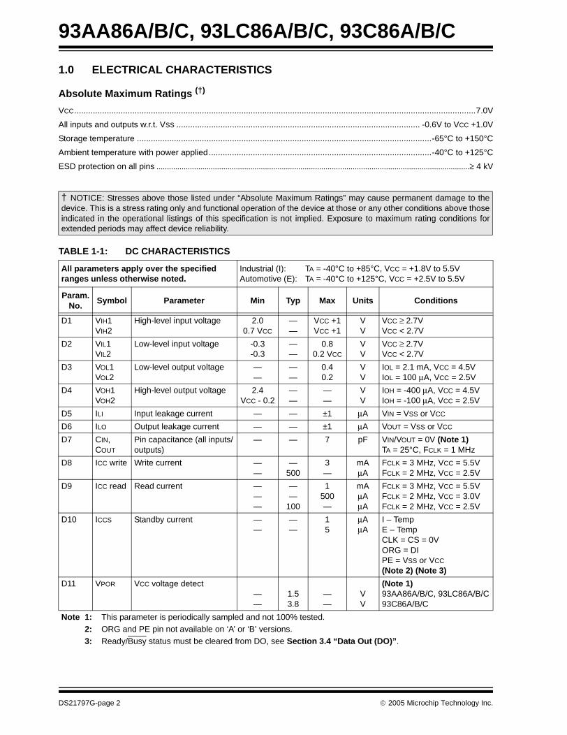
TABLE 1-1: DC CHARACTERISTICS
† NOTICE: Stresses above those listed under “Absolute Maximum Ratings” may cause permanent damage to thedevice. This is a stress rating only and functional operation of the device at those or any other conditions above thoseindicated in the operational listings of this specification is not implied. Exposure to maximum rating conditions forextended periods may affect device reliability.
All parameters apply over the specified ranges unless otherwise noted.
Industrial (I): TA = -40°C to +85°C, VCC = +1.8V to 5.5VAutomotive (E): TA = -40°C to +125°C, VCC = +2.5V to 5.5V
Param. No.
Symbol Parameter Min Typ Max Units Conditions
D1 VIH1VIH2
High-level input voltage 2.00.7 VCC
——
VCC +1VCC +1
VV
VCC ≥ 2.7VVCC < 2.7V
D2 VIL1VIL2
Low-level input voltage -0.3-0.3
——
0.80.2 VCC
VV
VCC ≥ 2.7VVCC < 2.7V
D3 VOL1VOL2
Low-level output voltage ——
——
0.40.2
VV
IOL = 2.1 mA, VCC = 4.5VIOL = 100 μA, VCC = 2.5V
D4 VOH1VOH2
High-level output voltage 2.4VCC - 0.2
——
——
VV
IOH = -400 μA, VCC = 4.5VIOH = -100 μA, VCC = 2.5V
D5 ILI Input leakage current — — ±1 μA VIN = VSS or VCC
D6 ILO Output leakage current — — ±1 μA VOUT = VSS or VCC
D7 CIN, COUT
Pin capacitance (all inputs/outputs)
— — 7 pF VIN/VOUT = 0V (Note 1)TA = 25°C, FCLK = 1 MHz
D8 ICC write Write current ——
—500
3—
mAμA
FCLK = 3 MHz, VCC = 5.5VFCLK = 2 MHz, VCC = 2.5V
D9 ICC read Read current ———
——
100
1500—
mAμAμA
FCLK = 3 MHz, VCC = 5.5VFCLK = 2 MHz, VCC = 3.0VFCLK = 2 MHz, VCC = 2.5V
D10 ICCS Standby current ——
——
15
μAμA
I – TempE – TempCLK = CS = 0VORG = DI PE = VSS or VCC
(Note 2) (Note 3)
D11 VPOR VCC voltage detect——
1.53.8
——
VV
(Note 1)93AA86A/B/C, 93LC86A/B/C93C86A/B/C
Note 1: This parameter is periodically sampled and not 100% tested.2: ORG and PE pin not available on ‘A’ or ‘B’ versions.3: Ready/Busy status must be cleared from DO, see Section 3.4 “Data Out (DO)”.
DS21797G-page 2 © 2005 Microchip Technology Inc.
93AA86A/B/C, 93LC86A/B/C, 93C86A/B/C
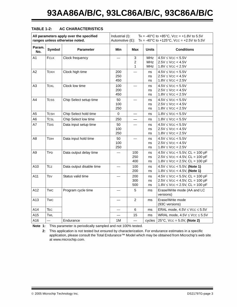
TABLE 1-2: AC CHARACTERISTICS
All parameters apply over the specified ranges unless otherwise noted.
Industrial (I): TA = -40°C to +85°C, VCC = +1.8V to 5.5VAutomotive (E): TA = -40°C to +125°C, VCC = +2.5V to 5.5V
Param. No.
Symbol Parameter Min Max Units Conditions
A1 FCLK Clock frequency — 321
MHzMHzMHz
4.5V ≤ VCC < 5.5V2.5V ≤ VCC < 4.5V1.8V ≤ VCC < 2.5V
A2 TCKH Clock high time 200250450
— nsnsns
4.5V ≤ VCC < 5.5V2.5V ≤ VCC < 4.5V1.8V ≤ VCC < 2.5V
A3 TCKL Clock low time 100200450
— nsnsns
4.5V ≤ VCC < 5.5V2.5V ≤ VCC < 4.5V1.8V ≤ VCC < 2.5V
A4 TCSS Chip Select setup time 50100250
— nsnsns
4.5V ≤ VCC < 5.5V2.5V ≤ VCC < 4.5V1.8V ≤ VCC < 2.5V
A5 TCSH Chip Select hold time 0 — ns 1.8V ≤ VCC < 5.5V
A6 TCSL Chip Select low time 250 — ns 1.8V ≤ VCC < 5.5V
A7 TDIS Data input setup time 50100250
— nsnsns
4.5V ≤ VCC < 5.5V2.5V ≤ VCC < 4.5V1.8V ≤ VCC < 2.5V
A8 TDIH Data input hold time 50100250
— nsnsns
4.5V ≤ VCC < 5.5V2.5V ≤ VCC < 4.5V1.8V ≤ VCC < 2.5V
A9 TPD Data output delay time — 100250400
nsnsns
4.5V ≤ VCC < 5.5V, CL = 100 pF2.5V ≤ VCC < 4.5V, CL = 100 pF1.8V ≤ VCC < 2.5V, CL = 100 pF
A10 TCZ Data output disable time — 100200
nsns
4.5V ≤ VCC < 5.5V, (Note 1)1.8V ≤ VCC < 4.5V, (Note 1)
A11 TSV Status valid time — 200300500
nsnsns
4.5V ≤ VCC < 5.5V, CL = 100 pF2.5V ≤ VCC < 4.5V, CL = 100 pF1.8V ≤ VCC < 2.5V, CL = 100 pF
A12 TWC Program cycle time — 5 ms Erase/Write mode (AA and LC versions)
A13 TWC — 2 ms Erase/Write mode (93C versions)
A14 TEC — 6 ms ERAL mode, 4.5V ≤ VCC ≤ 5.5V
A15 TWL — 15 ms WRAL mode, 4.5V ≤ VCC ≤ 5.5V
A16 — Endurance 1M — cycles 25°C, VCC = 5.0V, (Note 2)
Note 1: This parameter is periodically sampled and not 100% tested.
2: This application is not tested but ensured by characterization. For endurance estimates in a specific application, please consult the Total Endurance™ Model which may be obtained from Microchip’s web site at www.microchip.com.
© 2005 Microchip Technology Inc. DS21797G-page 3
93AA86A/B/C, 93LC86A/B/C, 93C86A/B/C
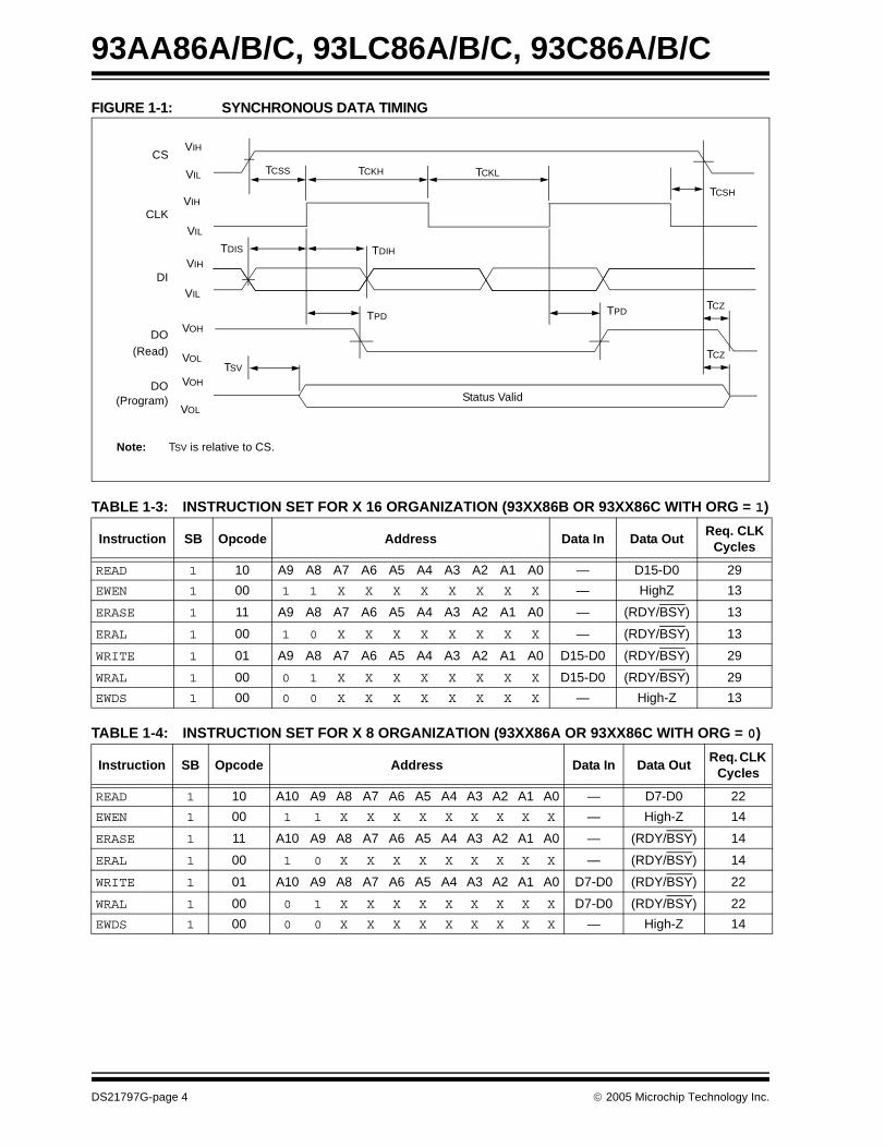
FIGURE 1-1: SYNCHRONOUS DATA TIMING
TABLE 1-3: INSTRUCTION SET FOR X 16 ORGANIZATION (93XX86B OR 93XX86C WITH ORG = 1)
TABLE 1-4: INSTRUCTION SET FOR X 8 ORGANIZATION (93XX86A OR 93XX86C WITH ORG = 0)
Instruction SB Opcode Address Data In Data OutReq. CLK
Cycles
READ 1 10 A9 A8 A7 A6 A5 A4 A3 A2 A1 A0 — D15-D0 29
EWEN 1 00 1 1 X X X X X X X X — HighZ 13
ERASE 1 11 A9 A8 A7 A6 A5 A4 A3 A2 A1 A0 — (RDY/BSY) 13
ERAL 1 00 1 0 X X X X X X X X — (RDY/BSY) 13
WRITE 1 01 A9 A8 A7 A6 A5 A4 A3 A2 A1 A0 D15-D0 (RDY/BSY) 29
WRAL 1 00 0 1 X X X X X X X X D15-D0 (RDY/BSY) 29
EWDS 1 00 0 0 X X X X X X X X — High-Z 13
Instruction SB Opcode Address Data In Data OutReq. CLK
Cycles
READ 1 10 A10 A9 A8 A7 A6 A5 A4 A3 A2 A1 A0 — D7-D0 22
EWEN 1 00 1 1 X X X X X X X X X — High-Z 14
ERASE 1 11 A10 A9 A8 A7 A6 A5 A4 A3 A2 A1 A0 — (RDY/BSY) 14
ERAL 1 00 1 0 X X X X X X X X X — (RDY/BSY) 14
WRITE 1 01 A10 A9 A8 A7 A6 A5 A4 A3 A2 A1 A0 D7-D0 (RDY/BSY) 22
WRAL 1 00 0 1 X X X X X X X X X D7-D0 (RDY/BSY) 22
EWDS 1 00 0 0 X X X X X X X X X — High-Z 14
CSVIH
VIL
VIH
VIL
VIH
VIL
VOH
VOL
VOH
VOL
CLK
DI
DO(Read)
DO(Program)
TCSS
TDIS
TCKH TCKL
TDIH
TPD
TCSH
TPD
TCZ
Status Valid
TSV
TCZ
Note: TSV is relative to CS.
DS21797G-page 4 © 2005 Microchip Technology Inc.
93AA86A/B/C, 93LC86A/B/C, 93C86A/B/C
2.0 FUNCTIONAL DESCRIPTION
When the ORG pin (93XX86C) is connected to VCC,the (x16) organization is selected. When it is connectedto ground, the (x8) organization is selected. Instruc-tions, addresses and write data are clocked into the DIpin on the rising edge of the clock (CLK). The DO pin isnormally held in a High-Z state except when readingdata from the device, or when checking the Ready/Busy status during a programming operation. TheReady/Busy status can be verified during an Erase/Write operation by polling the DO pin; DO low indicatesthat programming is still in progress, while DO highindicates the device is ready. DO will enter the High-Zstate on the falling edge of CS.
2.1 Start Condition
The Start bit is detected by the device if CS and DI areboth high with respect to the positive edge of CLK forthe first time.
Before a Start condition is detected, CS, CLK and DImay change in any combination (except to that of aStart condition), without resulting in any deviceoperation (Read, Write, Erase, EWEN, EWDS, ERALor WRAL). As soon as CS is high, the device is nolonger in Standby mode.
An instruction following a Start condition will only beexecuted if the required opcode, address and data bitsfor any particular instruction are clocked in.
2.2 Data In/Data Out (DI/DO)
It is possible to connect the Data In and Data Out pinstogether. However, with this configuration it is possiblefor a “bus conflict” to occur during the “dummy zero”that precedes the read operation, if A0 is a logic highlevel. Under such a condition the voltage level seen atData Out is undefined and will depend upon the relativeimpedances of Data Out and the signal source drivingA0. The higher the current sourcing capability of thedriver, the higher the voltage at the Data Out pin. Inorder to limit this current, a resistor should beconnected between DI and DO.
2.3 Data Protection
All modes of operation are inhibited when VCC is belowa typical voltage of 1.5V for ‘93AA’ and ‘93LC’ devicesor 3.8V for ‘93C’ devices.
The EWEN and EWDS commands give additionalprotection against accidentally programming duringnormal operation.
After power-up the device is automatically in the EWDSmode. Therefore, an EWEN instruction must beperformed before the initial ERASE or WRITE instructioncan be executed.Note: When preparing to transmit an instruction,
either the CLK or DI signal levels must beat a logic low as CS is toggled active high.
Note: For added protection, an EWDScommand should be performed afterevery write operation and an external 10kΩ pull-down protection resistor should beadded to the CS pin.
Note: To prevent accidental writes to the array inthe 93XX86C devices, set the PE pin to alogic low.
© 2005 Microchip Technology Inc. DS21797G-page 5
93AA86A/B/C, 93LC86A/B/C, 93C86A/B/C
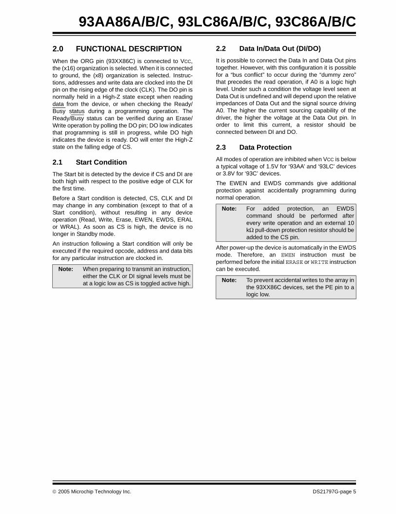
Block Diagram
MemoryArray
Data Register
ModeDecodeLogic
ClockRegister
AddressDecoder
AddressCounter
OutputBuffer
DO
DI
ORG*CS
CLK
VCC VSS
*ORG and PE inputs are not available on
PE*
A/B devices.
DS21797G-page 6 © 2005 Microchip Technology Inc.
93AA86A/B/C, 93LC86A/B/C, 93C86A/B/C
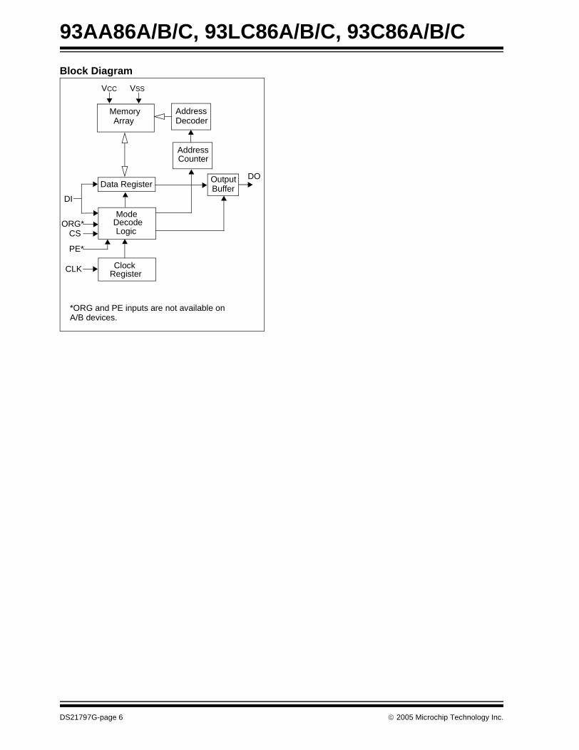
2.4 Erase
The ERASE instruction forces all data bits of the specified address to the logical ‘1’ state. The rising edge of CLK before the last address bit initiates the write cycle.
The DO pin indicates the Ready/Busy status of thedevice if CS is brought high after a minimum of 250 nslow (TCSL). DO at logical ‘0’ indicates that programmingis still in progress. DO at logical ‘1’ indicates that theregister at the specified address has been erased andthe device is ready for another instruction.
FIGURE 2-1: ERASE TIMING
Note: After the Erase cycle is complete, issuinga Start bit and then taking CS low will clearthe Ready/Busy status from DO.
CS
CLK
DI
DO
TCSL
Check Status
1 1 1 AN AN-1 AN-2 ••• A0
TSV TCZ
Busy ReadyHigh-Z
TWC
High-Z
© 2005 Microchip Technology Inc. DS21797G-page 7
93AA86A/B/C, 93LC86A/B/C, 93C86A/B/C
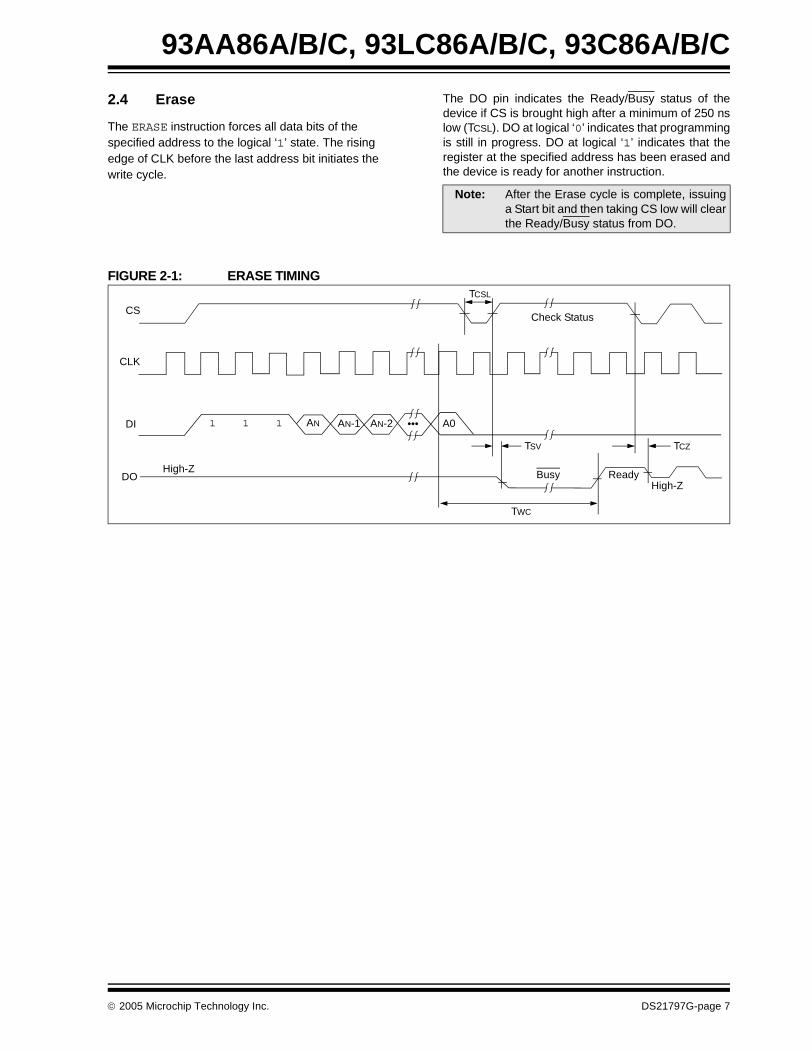
2.5 Erase All (ERAL)
The Erase All (ERAL) instruction will erase the entirememory array to the logical ‘1’ state. The ERAL cycleis identical to the erase cycle, except for the differentopcode. The ERAL cycle is completely self-timed. Therising edge of CLK before the last data bit initiates thewrite cycle. Clocking of the CLK pin is not necessaryafter the device has entered the ERAL cycle.
The DO pin indicates the Ready/Busy status of thedevice, if CS is brought high after a minimum of 250 nslow (TCSL).
VCC must be ≥ 4.5V for proper operation of ERAL.
FIGURE 2-2: ERAL TIMING
Note: After the ERAL command is complete,issuing a Start bit and then taking CS lowwill clear the Ready/Busy status from DO.
CS
CLK
DI
DO
TCSL
Check Status
1 0 0 1 0 x ••• x
TSV TCZ
Busy ReadyHigh-Z
TEC
High-Z
DS21797G-page 8 © 2005 Microchip Technology Inc.
93AA86A/B/C, 93LC86A/B/C, 93C86A/B/C
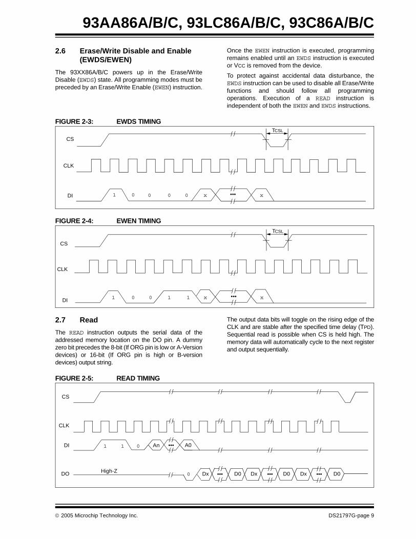
2.6 Erase/Write Disable and Enable (EWDS/EWEN)
The 93XX86A/B/C powers up in the Erase/WriteDisable (EWDS) state. All programming modes must bepreceded by an Erase/Write Enable (EWEN) instruction.
Once the EWEN instruction is executed, programmingremains enabled until an EWDS instruction is executedor VCC is removed from the device.
To protect against accidental data disturbance, theEWDS instruction can be used to disable all Erase/Writefunctions and should follow all programmingoperations. Execution of a READ instruction isindependent of both the EWEN and EWDS instructions.
FIGURE 2-3: EWDS TIMING
FIGURE 2-4: EWEN TIMING
2.7 Read
The READ instruction outputs the serial data of theaddressed memory location on the DO pin. A dummyzero bit precedes the 8-bit (If ORG pin is low or A-Versiondevices) or 16-bit (If ORG pin is high or B-versiondevices) output string.
The output data bits will toggle on the rising edge of theCLK and are stable after the specified time delay (TPD).Sequential read is possible when CS is held high. Thememory data will automatically cycle to the next registerand output sequentially.
FIGURE 2-5: READ TIMING
CS
CLK
DI 1 0 0 0 0 x ••• x
TCSL
1 x
CS
CLK
DI 0 0 1 1 x
TCSL
•••
CS
CLK
DI
DO
1 1 0 An ••• A0
High-Z0 Dx ••• D0 Dx ••• D0 •••Dx D0
© 2005 Microchip Technology Inc. DS21797G-page 9
93AA86A/B/C, 93LC86A/B/C, 93C86A/B/C
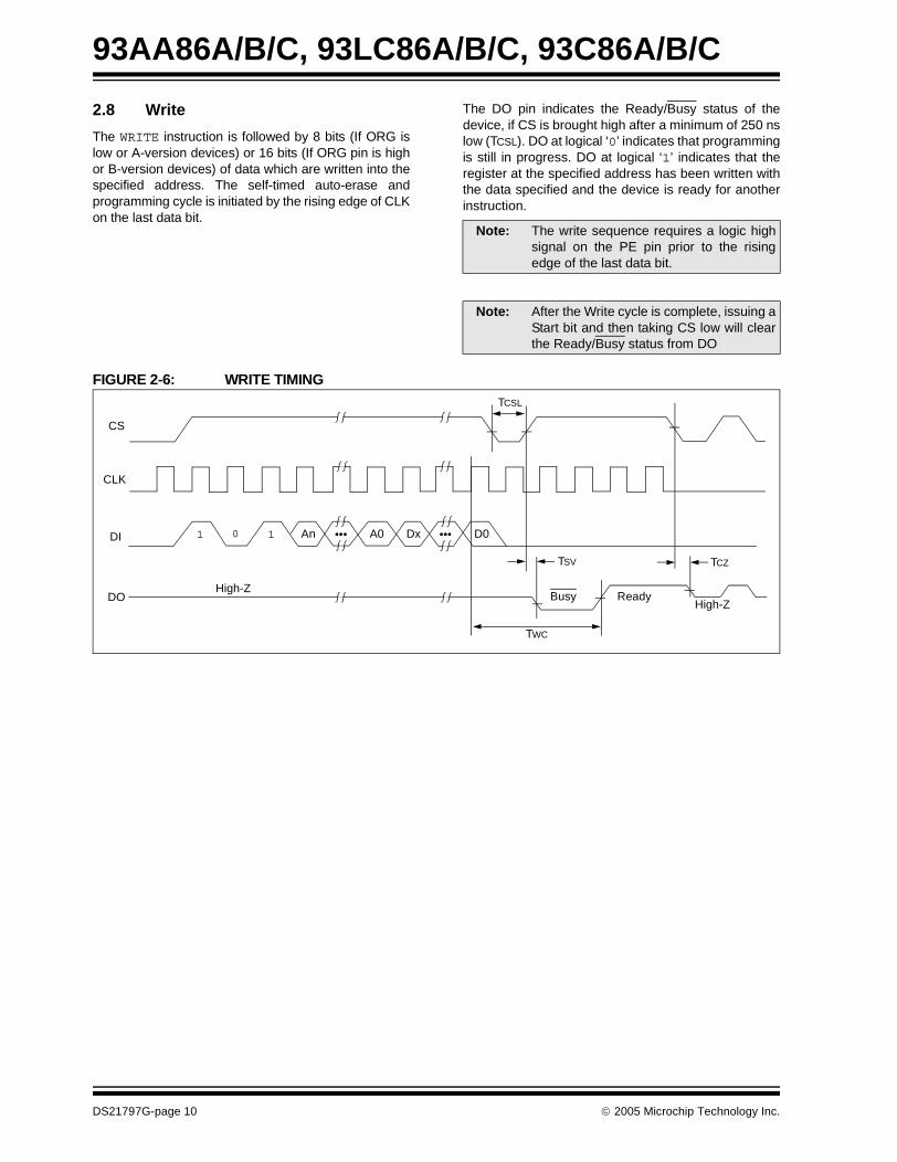
2.8 Write
The WRITE instruction is followed by 8 bits (If ORG islow or A-version devices) or 16 bits (If ORG pin is highor B-version devices) of data which are written into thespecified address. The self-timed auto-erase andprogramming cycle is initiated by the rising edge of CLKon the last data bit.
The DO pin indicates the Ready/Busy status of thedevice, if CS is brought high after a minimum of 250 nslow (TCSL). DO at logical ‘0’ indicates that programmingis still in progress. DO at logical ‘1’ indicates that theregister at the specified address has been written withthe data specified and the device is ready for anotherinstruction.
FIGURE 2-6: WRITE TIMING
Note: The write sequence requires a logic highsignal on the PE pin prior to the risingedge of the last data bit.
Note: After the Write cycle is complete, issuing aStart bit and then taking CS low will clearthe Ready/Busy status from DO
CS
CLK
DI
DO
1 0 1 An ••• A0 Dx ••• D0
Busy ReadyHigh-Z
High-Z
TWC
TCSL
TCZTSV
DS21797G-page 10 © 2005 Microchip Technology Inc.
93AA86A/B/C, 93LC86A/B/C, 93C86A/B/C
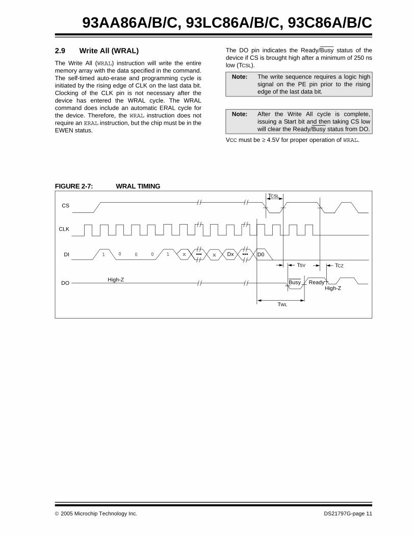
2.9 Write All (WRAL)
The Write All (WRAL) instruction will write the entirememory array with the data specified in the command.The self-timed auto-erase and programming cycle isinitiated by the rising edge of CLK on the last data bit.Clocking of the CLK pin is not necessary after thedevice has entered the WRAL cycle. The WRALcommand does include an automatic ERAL cycle forthe device. Therefore, the WRAL instruction does notrequire an ERAL instruction, but the chip must be in theEWEN status.
The DO pin indicates the Ready/Busy status of thedevice if CS is brought high after a minimum of 250 nslow (TCSL).
VCC must be ≥ 4.5V for proper operation of WRAL.
FIGURE 2-7: WRAL TIMING
Note: The write sequence requires a logic highsignal on the PE pin prior to the risingedge of the last data bit.
Note: After the Write All cycle is complete,issuing a Start bit and then taking CS lowwill clear the Ready/Busy status from DO.
CS
CLK
DI
DOHigh-Z
1 0 0 0 1 x ••• x Dx ••• D0
High-Z Busy Ready
TWL
TCSL
TSV TCZ
© 2005 Microchip Technology Inc. DS21797G-page 11
93AA86A/B/C, 93LC86A/B/C, 93C86A/B/C
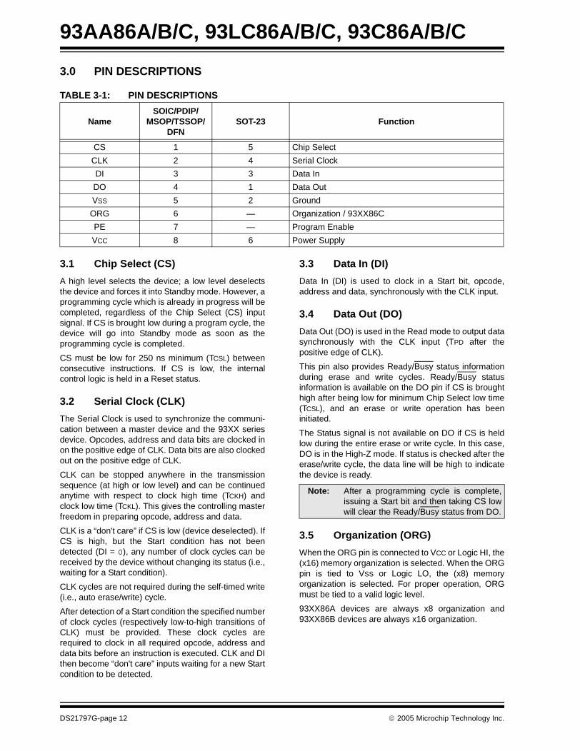
3.0 PIN DESCRIPTIONS
TABLE 3-1: PIN DESCRIPTIONS
3.1 Chip Select (CS)
A high level selects the device; a low level deselectsthe device and forces it into Standby mode. However, aprogramming cycle which is already in progress will becompleted, regardless of the Chip Select (CS) inputsignal. If CS is brought low during a program cycle, thedevice will go into Standby mode as soon as theprogramming cycle is completed.
CS must be low for 250 ns minimum (TCSL) betweenconsecutive instructions. If CS is low, the internalcontrol logic is held in a Reset status.
3.2 Serial Clock (CLK)
The Serial Clock is used to synchronize the communi-cation between a master device and the 93XX seriesdevice. Opcodes, address and data bits are clocked inon the positive edge of CLK. Data bits are also clockedout on the positive edge of CLK.
CLK can be stopped anywhere in the transmissionsequence (at high or low level) and can be continuedanytime with respect to clock high time (TCKH) andclock low time (TCKL). This gives the controlling masterfreedom in preparing opcode, address and data.
CLK is a “don't care” if CS is low (device deselected). IfCS is high, but the Start condition has not beendetected (DI = 0), any number of clock cycles can bereceived by the device without changing its status (i.e.,waiting for a Start condition).
CLK cycles are not required during the self-timed write(i.e., auto erase/write) cycle.
After detection of a Start condition the specified numberof clock cycles (respectively low-to-high transitions ofCLK) must be provided. These clock cycles arerequired to clock in all required opcode, address anddata bits before an instruction is executed. CLK and DIthen become “don't care” inputs waiting for a new Startcondition to be detected.
3.3 Data In (DI)
Data In (DI) is used to clock in a Start bit, opcode,address and data, synchronously with the CLK input.
3.4 Data Out (DO)
Data Out (DO) is used in the Read mode to output datasynchronously with the CLK input (TPD after thepositive edge of CLK).
This pin also provides Ready/Busy status informationduring erase and write cycles. Ready/Busy statusinformation is available on the DO pin if CS is broughthigh after being low for minimum Chip Select low time(TCSL), and an erase or write operation has beeninitiated.
The Status signal is not available on DO if CS is heldlow during the entire erase or write cycle. In this case,DO is in the High-Z mode. If status is checked after theerase/write cycle, the data line will be high to indicatethe device is ready.
3.5 Organization (ORG)
When the ORG pin is connected to VCC or Logic HI, the(x16) memory organization is selected. When the ORGpin is tied to VSS or Logic LO, the (x8) memoryorganization is selected. For proper operation, ORGmust be tied to a valid logic level.
93XX86A devices are always x8 organization and93XX86B devices are always x16 organization.
NameSOIC/PDIP/
MSOP/TSSOP/DFN
SOT-23 Function
CS 1 5 Chip Select
CLK 2 4 Serial Clock
DI 3 3 Data In
DO 4 1 Data Out
VSS 5 2 Ground
ORG 6 — Organization / 93XX86C
PE 7 — Program Enable
VCC 8 6 Power Supply
Note: After a programming cycle is complete,issuing a Start bit and then taking CS lowwill clear the Ready/Busy status from DO.
DS21797G-page 12 © 2005 Microchip Technology Inc.
93AA86A/B/C, 93LC86A/B/C, 93C86A/B/C
3.6 Program Enable (PE)
This pin allows the user to enable or disable the abilityto write data to the memory array. If the PE pin is tiedto VCC, the device can be programmed. If the PE pin istied to VSS, programming will be inhibited. This pincannot be floated, it must be tied to VCC or VSS. PE isnot available on 93XX86A or 93XX86B. On thosedevices, programming is always enabled.
© 2005 Microchip Technology Inc. DS21797G-page 13
93AA86A/B/C, 93LC86A/B/C, 93C86A/B/C
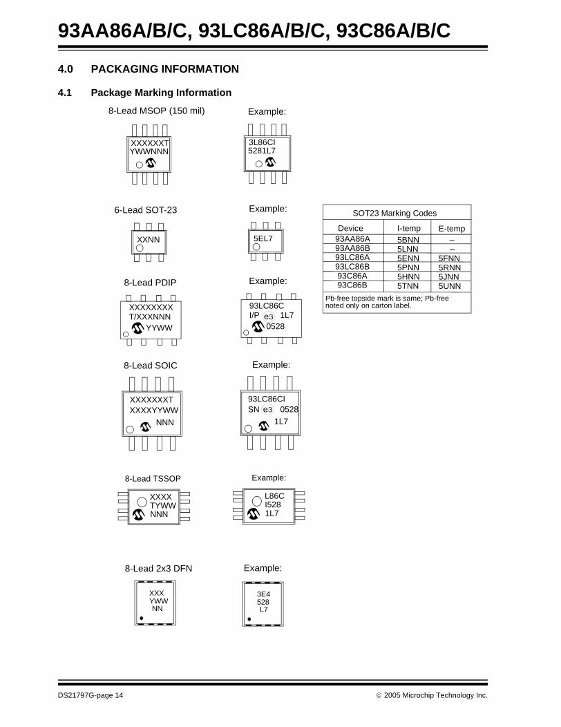
4.0 PACKAGING INFORMATION
4.1 Package Marking Information
Example:6-Lead SOT-23
8-Lead MSOP (150 mil) Example:
XXXXXXTYWWNNN
3L86CI 5281L7
XXNN 5EL7
T/XXXNNNXXXXXXXX
YYWW
8-Lead PDIP
8-Lead SOIC
XXXXYYWWXXXXXXXT
NNN
XXXXTYWW
8-Lead TSSOP
NNN
I/P 1L793LC86C
0528
Example:
Example:
SN 052893LC86CI
1L7
1L7
L86CI528
Example:
SOT23 Marking Codes
Device93AA86A93AA86B93LC86A93LC86B93C86A93C86B
I-temp5BNN5LNN5ENN5PNN5HNN5TNN
E-temp––
5FNN5RNN5JNN5UNN
Pb-free topside mark is same; Pb-freenoted only on carton label.
3e
3e
8-Lead 2x3 DFN
3E4528L7
Example:
XXXYWWNN
DS21797G-page 14 © 2005 Microchip Technology Inc.
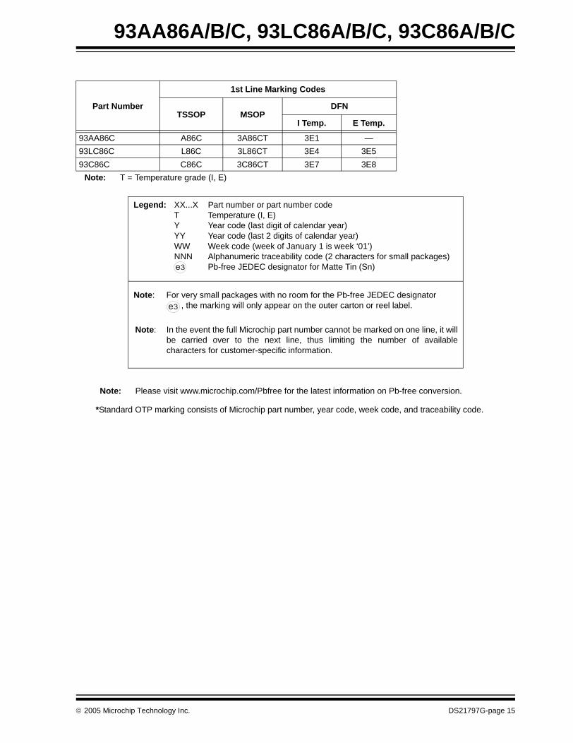
93AA86A/B/C, 93LC86A/B/C, 93C86A/B/C
Part Number
1st Line Marking Codes
TSSOP MSOPDFN
I Temp. E Temp.
93AA86C A86C 3A86CT 3E1 —
93LC86C L86C 3L86CT 3E4 3E5
93C86C C86C 3C86CT 3E7 3E8
Note: T = Temperature grade (I, E)
Legend: XX...X Part number or part number codeT Temperature (I, E)Y Year code (last digit of calendar year)YY Year code (last 2 digits of calendar year)WW Week code (week of January 1 is week ‘01’)NNN Alphanumeric traceability code (2 characters for small packages)
Pb-free JEDEC designator for Matte Tin (Sn)
Note: For very small packages with no room for the Pb-free JEDEC designator , the marking will only appear on the outer carton or reel label.
Note: In the event the full Microchip part number cannot be marked on one line, it willbe carried over to the next line, thus limiting the number of availablecharacters for customer-specific information.
3e
3e
Note: Please visit www.microchip.com/Pbfree for the latest information on Pb-free conversion.
*Standard OTP marking consists of Microchip part number, year code, week code, and traceability code.
© 2005 Microchip Technology Inc. DS21797G-page 15
93AA86A/B/C, 93LC86A/B/C, 93C86A/B/C
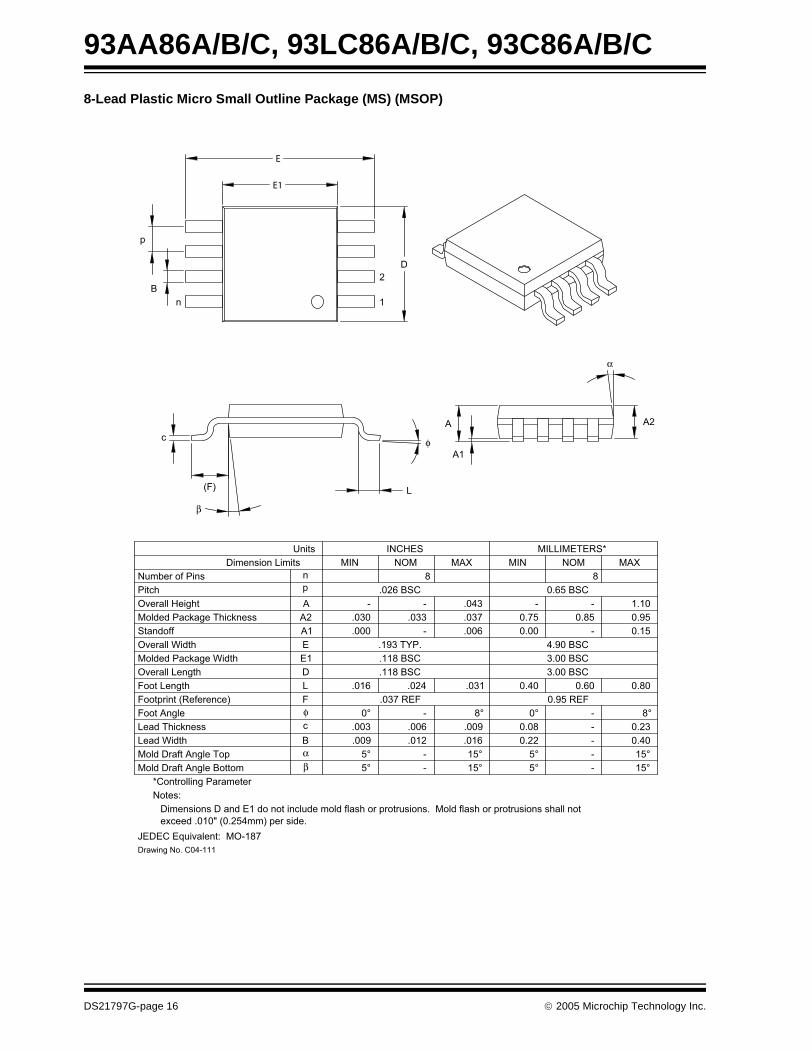
8-Lead Plastic Micro Small Outline Package (MS) (MSOP)
D
A
A1
L
c
(F)
α
A2
E1
E
p
B
n 1
2
φ
β
Dimensions D and E1 do not include mold flash or protrusions. Mold flash or protrusions shall not
.037 REFFFootprint (Reference)
exceed .010" (0.254mm) per side.
Notes:
Drawing No. C04-111
*Controlling Parameter
Mold Draft Angle Top
Mold Draft Angle Bottom
Foot Angle
Lead Width
Lead Thickness
βα
c
B
φ.003
.009
.006
.012
Dimension Limits
Overall Height
Molded Package Thickness
Molded Package Width
Overall Length
Foot Length
Standoff
Overall Width
Number of Pins
Pitch
A
L
E1
D
A1
E
A2
.016 .024
.118 BSC
.118 BSC
.000
.030
.193 TYP.
.033
MIN
p
n
Units
.026 BSC
NOM
8
INCHES
0.95 REF
-
-
.009
.016
0.08
0.22
0°
0.23
0.40
8°
MILLIMETERS*
0.65 BSC
0.85
3.00 BSC
3.00 BSC
0.60
4.90 BSC
.043
.031
.037
.006
0.40
0.00
0.75
MINMAX NOM
1.10
0.80
0.15
0.95
MAX
8
- -
-
15°5° -
15°5° -
JEDEC Equivalent: MO-187
0° - 8°
5°
5° -
-
15°
15°
--
- -
DS21797G-page 16 © 2005 Microchip Technology Inc.
93AA86A/B/C, 93LC86A/B/C, 93C86A/B/C
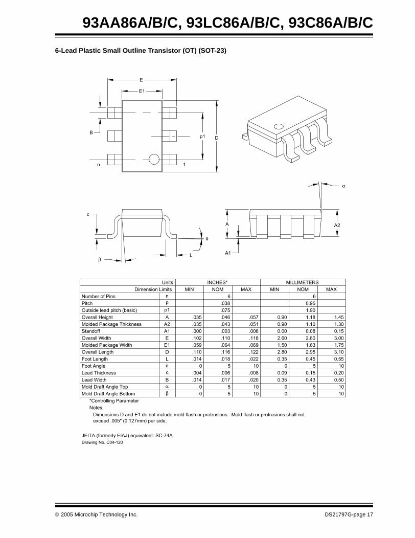
6-Lead Plastic Small Outline Transistor (OT) (SOT-23)
10501050βMold Draft Angle Bottom
10501050αMold Draft Angle Top
0.500.430.35.020.017.014BLead Width
0.200.150.09.008.006.004cLead Thickness
10501050φFoot Angle
0.550.450.35.022.018.014LFoot Length
3.102.952.80.122.116.110DOverall Length
1.751.631.50.069.064.059E1Molded Package Width
3.002.802.60.118.110.102EOverall Width
0.150.080.00.006.003.000A1Standoff
1.301.100.90.051.043.035A2Molded Package Thickness
1.451.180.90.057.046.035AOverall Height
1.90.075p1Outside lead pitch (basic)
0.95.038pPitch
66nNumber of Pins
MAXNOMMINMAXNOMMINDimension Limits
MILLIMETERSINCHES*Units
1
DB
n
E
E1
L
c
β
φ
α
A2A
A1
p1
exceed .005" (0.127mm) per side.
Dimensions D and E1 do not include mold flash or protrusions. Mold flash or protrusions shall not
Notes:
JEITA (formerly EIAJ) equivalent: SC-74A
Drawing No. C04-120
*Controlling Parameter
© 2005 Microchip Technology Inc. DS21797G-page 17
93AA86A/B/C, 93LC86A/B/C, 93C86A/B/C
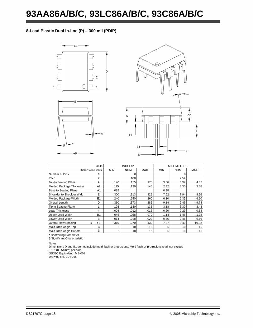
8-Lead Plastic Dual In-line (P) – 300 mil (PDIP)
B1
B
A1
A
L
A2
p
α
E
eB
β
c
E1
n
D
1
2
Units INCHES* MILLIMETERSDimension Limits MIN NOM MAX MIN NOM MAX
Number of Pins n 8 8Pitch p .100 2.54Top to Seating Plane A .140 .155 .170 3.56 3.94 4.32Molded Package Thickness A2 .115 .130 .145 2.92 3.30 3.68Base to Seating Plane A1 .015 0.38Shoulder to Shoulder Width E .300 .313 .325 7.62 7.94 8.26Molded Package Width E1 .240 .250 .260 6.10 6.35 6.60Overall Length D .360 .373 .385 9.14 9.46 9.78Tip to Seating Plane L .125 .130 .135 3.18 3.30 3.43Lead Thickness c .008 .012 .015 0.20 0.29 0.38Upper Lead Width B1 .045 .058 .070 1.14 1.46 1.78Lower Lead Width B .014 .018 .022 0.36 0.46 0.56Overall Row Spacing § eB .310 .370 .430 7.87 9.40 10.92Mold Draft Angle Top α 5 10 15 5 10 15Mold Draft Angle Bottom β 5 10 15 5 10 15* Controlling Parameter
Notes:Dimensions D and E1 do not include mold flash or protrusions. Mold flash or protrusions shall not exceed
JEDEC Equivalent: MS-001Drawing No. C04-018
.010” (0.254mm) per side.
§ Significant Characteristic
DS21797G-page 18 © 2005 Microchip Technology Inc.
93AA86A/B/C, 93LC86A/B/C, 93C86A/B/C
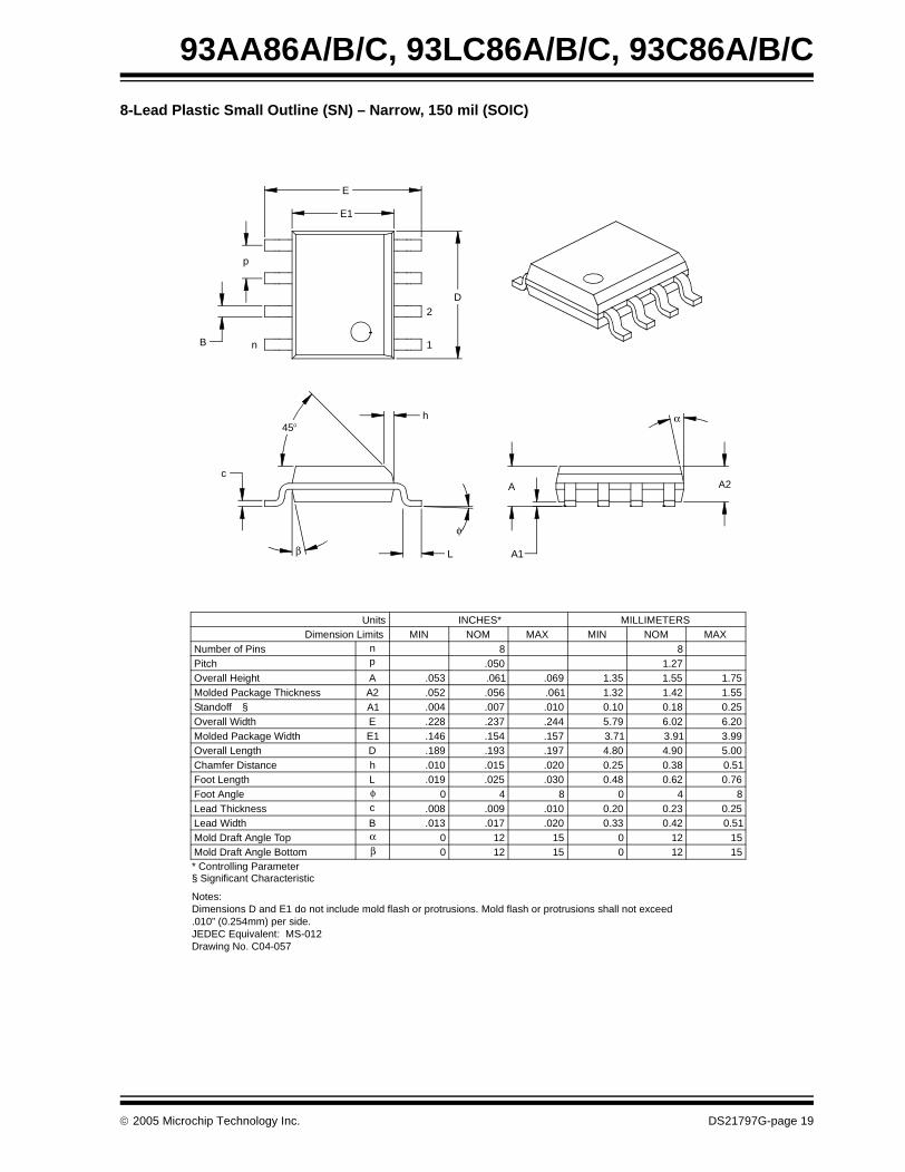
8-Lead Plastic Small Outline (SN) – Narrow, 150 mil (SOIC)
Foot Angle φ 0 4 8 0 4 8
1512015120βMold Draft Angle Bottom1512015120αMold Draft Angle Top
0.510.420.33.020.017.013BLead Width0.250.230.20.010.009.008cLead Thickness
0.760.620.48.030.025.019LFoot Length0.510.380.25.020.015.010hChamfer Distance5.004.904.80.197.193.189DOverall Length3.993.913.71.157.154.146E1Molded Package Width6.206.025.79.244.237.228EOverall Width0.250.180.10.010.007.004A1Standoff §1.551.421.32.061.056.052A2Molded Package Thickness1.751.551.35.069.061.053AOverall Height
1.27.050pPitch88nNumber of Pins
MAXNOMMINMAXNOMMINDimension LimitsMILLIMETERSINCHES*Units
2
1
D
n
p
B
E
E1
h
Lβ
c
45°
φ
A2
α
A
A1
* Controlling Parameter
Notes:Dimensions D and E1 do not include mold flash or protrusions. Mold flash or protrusions shall not exceed .010” (0.254mm) per side.JEDEC Equivalent: MS-012Drawing No. C04-057
§ Significant Characteristic
© 2005 Microchip Technology Inc. DS21797G-page 19
93AA86A/B/C, 93LC86A/B/C, 93C86A/B/C
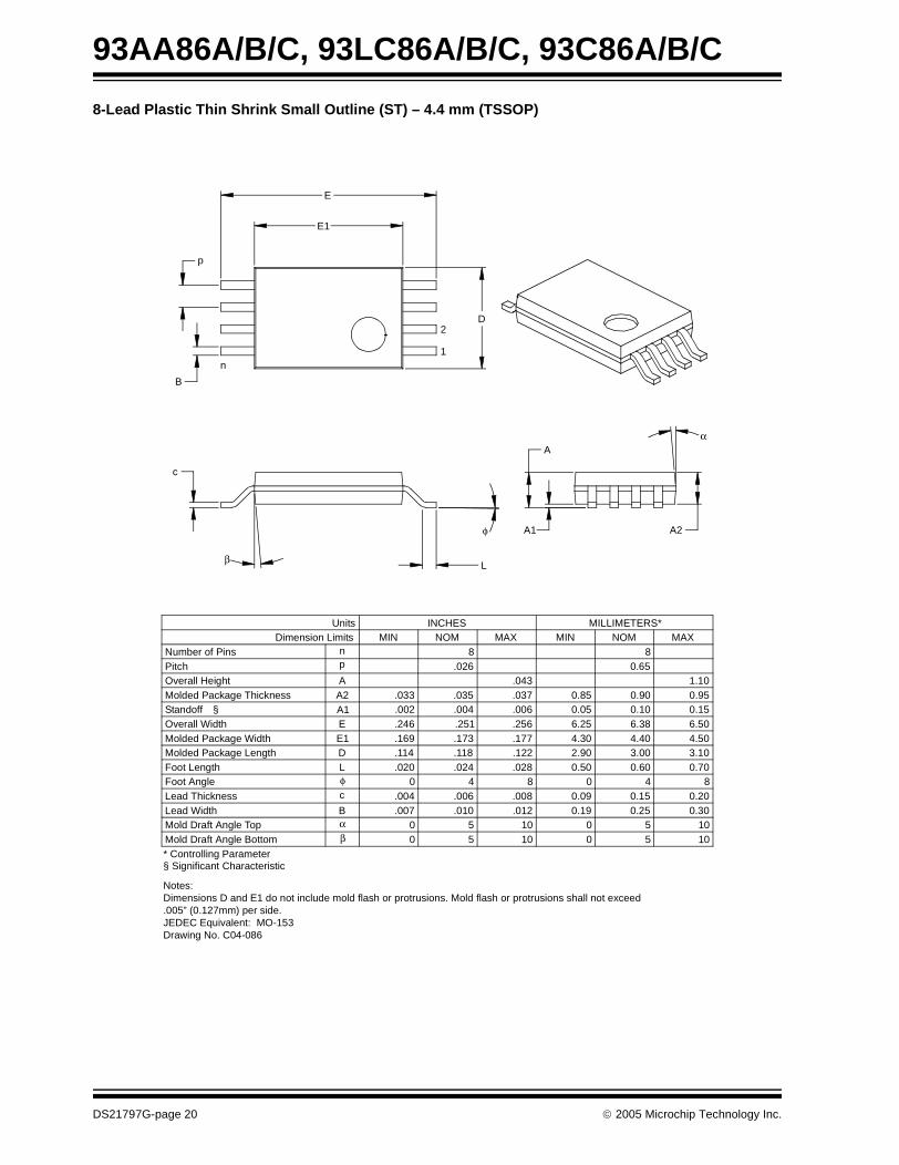
8-Lead Plastic Thin Shrink Small Outline (ST) – 4.4 mm (TSSOP)
10501050βMold Draft Angle Bottom10501050αMold Draft Angle Top
0.300.250.19.012.010.007BLead Width0.200.150.09.008.006.004cLead Thickness
0.700.600.50.028.024.020LFoot Length3.103.002.90.122.118.114DMolded Package Length4.504.404.30.177.173.169E1Molded Package Width6.506.386.25.256.251.246EOverall Width0.150.100.05.006.004.002A1Standoff §0.950.900.85.037.035.033A2Molded Package Thickness1.10.043AOverall Height
0.65.026pPitch88nNumber of Pins
MAXNOMMINMAXNOMMINDimension LimitsMILLIMETERS*INCHESUnits
α
A2
A
A1
L
c
β
φ
1
2D
n
p
B
E
E1
Foot Angle φ 0 4 8 0 4 8
* Controlling Parameter
Notes:Dimensions D and E1 do not include mold flash or protrusions. Mold flash or protrusions shall not exceed .005” (0.127mm) per side.JEDEC Equivalent: MO-153Drawing No. C04-086
§ Significant Characteristic
DS21797G-page 20 © 2005 Microchip Technology Inc.
93AA86A/B/C, 93LC86A/B/C, 93C86A/B/C
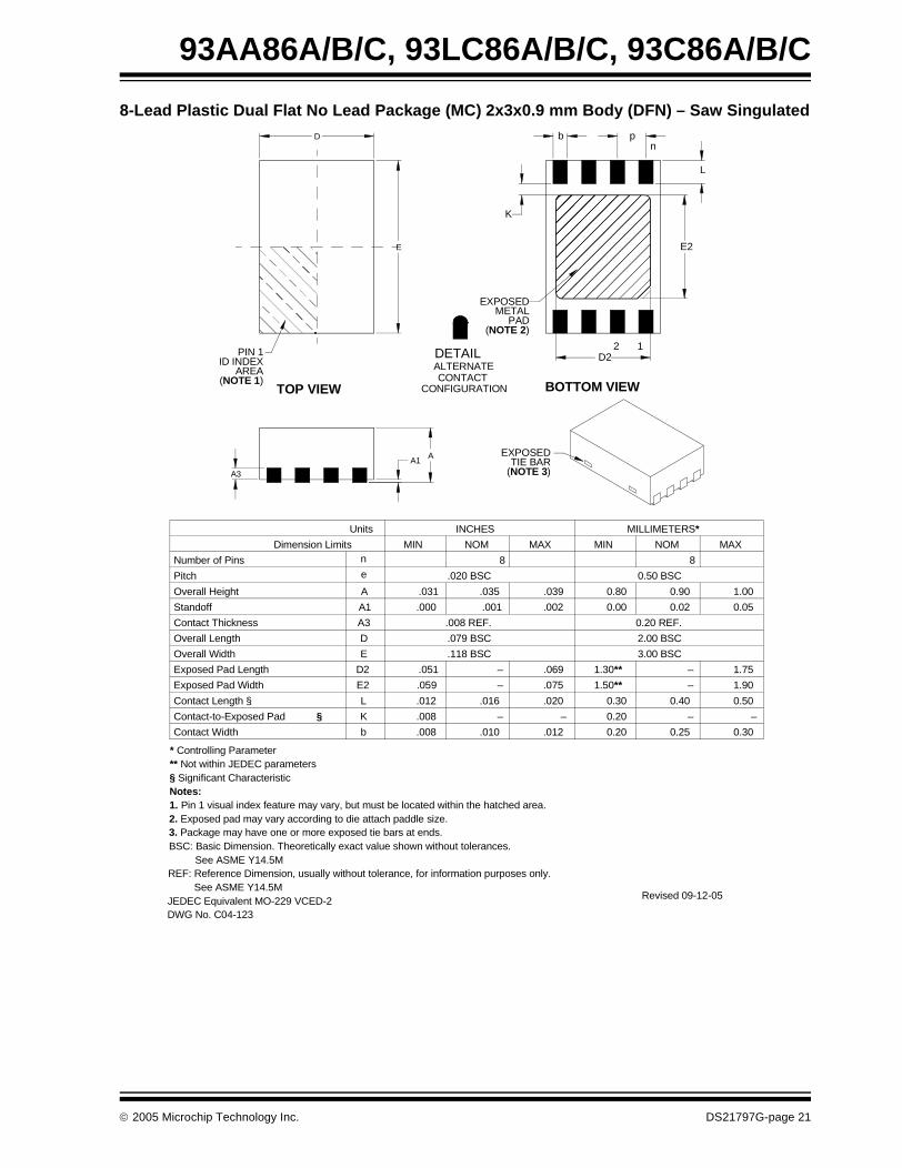
8-Lead Plastic Dual Flat No Lead Package (MC) 2x3x0.9 mm Body (DFN) – Saw Singulated
L
E2
A3
A1A
TOP VIEW
D
E
EXPOSED
PADMETAL
D2
BOTTOM VIEW
2 1
b pn
(NOTE 3)
EXPOSEDTIE BAR
PIN 1
(NOTE 1)
ID INDEXAREA
(NOTE 2)
CONFIGURATIONCONTACT
ALTERNATEDETAIL
K
3. Package may have one or more exposed tie bars at ends.BSC: Basic Dimension. Theoretically exact value shown without tolerances.
REF: Reference Dimension, usually without tolerance, for information purposes only.
JEDEC Equivalent MO-229 VCED-2See ASME Y14.5M
See ASME Y14.5M
MILLIMETERS*
0.50 BSC
2.00 BSC
0.20 REF.
3.00 BSC
1. Pin 1 visual index feature may vary, but must be located within the hatched area.
.039.035.031 0.80AOverall Height
2. Exposed pad may vary according to die attach paddle size.
* Controlling Parameter
Contact Length §
Notes:
Contact Width
Standoff
Overall Width
Overall Length
Contact Thickness
Exposed Pad Width
Exposed Pad Length
.010.008
L
b .012 0.20
.001
.008 REF.
.079 BSC
–
–
.118 BSC
D
.051
.059
D2
E2
E
.000
A3
A1
.069
.075
1.30**
1.50**
.002 0.00
Dimension Limits
Pitch
Number of Pins
INCHES
.020 BSC
MINn
e
NOM
Units
8
MAX MIN
1.000.90
0.25 0.30
–
–
1.75
1.90
0.02 0.05
8
NOM MAX
Contact-to-Exposed Pad §
.012
K
.016 0.40.020 0.30 0.50
** Not within JEDEC parameters§ Significant Characteristic
.008 – – 0.20 ––
DWG No. C04-123
Revised 09-12-05
© 2005 Microchip Technology Inc. DS21797G-page 21
93AA86A/B/C, 93LC86A/B/C, 93C86A/B/C
APPENDIX A: REVISION HISTORY
Revision C
Corrections to Section 1.0, Electrical Characteristics.Section 4.1, 6-Lead SOT-23 package to OT.
Revision D
Corrections to Device Selection Table, Table 1-1, Table1-2, Section 2.4, Section 2.5, Section 2.8 and Section2.9. Added note to Figure 2-7.
Revision E
Added DFN package.
Revision F
Added notes throughout.
Revision G
Revised note in Sections 2.8 and 2.9.Replaced DFN package drawing.
DS21797G-page 22 © 2005 Microchip Technology Inc.
93AA86A/B/C, 93LC86A/B/C, 93C86A/B/C
THE MICROCHIP WEB SITE
Microchip provides online support via our WWW site atwww.microchip.com. This web site is used as a meansto make files and information easily available tocustomers. Accessible by using your favorite Internetbrowser, the web site contains the followinginformation:
• Product Support – Data sheets and errata, application notes and sample programs, design resources, user’s guides and hardware support documents, latest software releases and archived software
• General Technical Support – Frequently Asked Questions (FAQ), technical support requests, online discussion groups, Microchip consultant program member listing
• Business of Microchip – Product selector and ordering guides, latest Microchip press releases, listing of seminars and events, listings of Microchip sales offices, distributors and factory representatives
CUSTOMER CHANGE NOTIFICATION SERVICE
Microchip’s customer notification service helps keepcustomers current on Microchip products. Subscriberswill receive e-mail notification whenever there arechanges, updates, revisions or errata related to aspecified product family or development tool of interest.
To register, access the Microchip web site atwww.microchip.com, click on Customer ChangeNotification and follow the registration instructions.
CUSTOMER SUPPORT
Users of Microchip products can receive assistancethrough several channels:
• Distributor or Representative
• Local Sales Office• Field Application Engineer (FAE)• Technical Support
• Development Systems Information Line
Customers should contact their distributor,representative or field application engineer (FAE) forsupport. Local sales offices are also available to helpcustomers. A listing of sales offices and locations isincluded in the back of this document.
Technical support is available through the web siteat: http://support.microchip.com
© 2005 Microchip Technology Inc. DS21797G-page 23

93AA86A/B/C, 93LC86A/B/C, 93C86A/B/C
READER RESPONSE
It is our intention to provide you with the best documentation possible to ensure successful use of your Microchip prod-uct. If you wish to provide your comments on organization, clarity, subject matter, and ways in which our documentationcan better serve you, please FAX your comments to the Technical Publications Manager at (480) 792-4150.
Please list the following information, and use this outline to provide us with your comments about this document.
To: Technical Publications Manager
RE: Reader Response
Total Pages Sent ________
From: Name
Company
Address
City / State / ZIP / Country
Telephone: (_______) _________ - _________
Application (optional):
Would you like a reply? Y N
Device: Literature Number:
Questions:
FAX: (______) _________ - _________
DS21797G93AA86A/B/C, 93LC86A/B/C, 93C86A/B/C
1. What are the best features of this document?
2. How does this document meet your hardware and software development needs?
3. Do you find the organization of this document easy to follow? If not, why?
4. What additions to the document do you think would enhance the structure and subject?
5. What deletions from the document could be made without affecting the overall usefulness?
6. Is there any incorrect or misleading information (what and where)?
7. How would you improve this document?
DS21797G-page 24 © 2005 Microchip Technology Inc.
93AA86A/B/C, 93LC86A/B/C, 93C86A/B/C
PRODUCT IDENTIFICATION SYSTEM
To order or obtain information, e.g., on pricing or delivery, refer to the factory or the listed sales office.
Note 1: Most products manufactured after January 2005 will have a Matte Tin (Pb-free) finish. Most products manufacturedbefore January 2005 will have a finish of approximately 63% Sn and 37% Pb (Sn/Pb). Please visit www.microchip.com for the latest information on Pb-free conversion, including conversion date codes.
Sales and Support
Data Sheets
Products supported by a preliminary Data Sheet may have an errata sheet describing minor operational differencesand recommended workarounds. To determine if an errata sheet exists for a particular device, please contact one ofthe following:
1. Your local Microchip sales office2. The Microchip Corporate Literature Center U.S. FAX: (480) 792-7277
3. The Microchip Worldwide Site (www.microchip.com)
Please specify which device, revision of silicon and Data Sheet (include Literature #) you are using.
New Customer Notification System
Register on our web site (www.microchip.com/cn) to receive the most current information on our products.
Device: 93AA86A: 16K 1.8V Microwire Serial EEPROM (x8)93AA86B: 16K 1.8V Microwire Serial EEPROM (x16)93AA86C: 16K 1.8V Microwire Serial EEPROM w/ORG
93LC86A: 16K 2.5V Microwire Serial EEPROM (x8)93LC86B: 16K 2.5V Microwire Serial EEPROM (x16)93LC86C: 16K 2.5V Microwire Serial EEPROM w/ORG
93C86A: 16K 5.0V Microwire Serial EEPROM (x8)93C86B: 16K 5.0V Microwire Serial EEPROM (x16)93C86C: 16K 5.0V Microwire Serial EEPROM w/ORG
Tape & Reel: Blank = Standard packagingT = Tape & Reel
Temperature Range: I = -40°C to +85°CE = -40°C to +125°C
Package: MS = Plastic MSOP (Micro Small outline, 8-lead)OT = SOT-23, 6-lead (Tape & Reel only)P = Plastic DIP (300 mil body), 8-leadSN = Plastic SOIC (150 mil body), 8-leadST = TSSOP, 8-leadMC = 2x3 DFN, 8-lead
Lead Finish: Blank = Pb-free - Matte Tin (see Note 1)G = Pb-free - Matte Tin only
Examples:
a) 93AA86C-I/MS: 16K, 2048x8 or 1024x16Serial EEPROM, MSOP package, 1.8V
b) 93AA86AT-I/OT: 16K, 2048x8 Serial EEPROM,SOT-23 package, tape and reel, 1.8V
c) 93AA86CT-I/MS: 16K, 2048x8 or 1024x16Serial EEPROM, MSOP package, tape andreel, 1.8V
a) 93LC86C-I/MS: 16K, 2048x8, 1024x16 SerialEEPROM, MSOP package, 2.5V
b) 93LC86BT-I/OT: 16K, 1024x16 SerialEEPROM, SOT-23 package, tape and reel,2.5V
a) 93C86C-I/MS: 16K, 2048x8 or 1024x16 SerialEEPROM, MSOP package, 5.0V
b) 93C86AT-I/OT: 16K, 2048x8 Serial EEPROM,SOT-23 package, tape and reel, 5.0V
PART NO. X /XX
PackageTemperatureRange
Device
X
Lead Finish
X
Tape & Reel
© 2005 Microchip Technology Inc. DS21797G-page 25
93AA86A/B/C, 93LC86A/B/C, 93C86A/B/C
NOTES:
DS21797G-page 26 © 2005 Microchip Technology Inc.
Note the following details of the code protection feature on Microchip devices:
• Microchip products meet the specification contained in their particular Microchip Data Sheet.
• Microchip believes that its family of products is one of the most secure families of its kind on the market today, when used in the intended manner and under normal conditions.
• There are dishonest and possibly illegal methods used to breach the code protection feature. All of these methods, to our knowledge, require using the Microchip products in a manner outside the operating specifications contained in Microchip’s Data Sheets. Most likely, the person doing so is engaged in theft of intellectual property.
• Microchip is willing to work with the customer who is concerned about the integrity of their code.
• Neither Microchip nor any other semiconductor manufacturer can guarantee the security of their code. Code protection does not mean that we are guaranteeing the product as “unbreakable.”
Code protection is constantly evolving. We at Microchip are committed to continuously improving the code protection features of ourproducts. Attempts to break Microchip’s code protection feature may be a violation of the Digital Millennium Copyright Act. If such actsallow unauthorized access to your software or other copyrighted work, you may have a right to sue for relief under that Act.
Information contained in this publication regarding deviceapplications and the like is provided only for your convenienceand may be superseded by updates. It is your responsibility toensure that your application meets with your specifications.MICROCHIP MAKES NO REPRESENTATIONS OR WAR-RANTIES OF ANY KIND WHETHER EXPRESS OR IMPLIED,WRITTEN OR ORAL, STATUTORY OR OTHERWISE,RELATED TO THE INFORMATION, INCLUDING BUT NOTLIMITED TO ITS CONDITION, QUALITY, PERFORMANCE,MERCHANTABILITY OR FITNESS FOR PURPOSE.Microchip disclaims all liability arising from this information andits use. Use of Microchip’s products as critical components inlife support systems is not authorized except with expresswritten approval by Microchip. No licenses are conveyed,implicitly or otherwise, under any Microchip intellectual propertyrights.
© 2005 Microchip Technology Inc.
Trademarks
The Microchip name and logo, the Microchip logo, Accuron, dsPIC, KEELOQ, microID, MPLAB, PIC, PICmicro, PICSTART, PRO MATE, PowerSmart, rfPIC, and SmartShunt are registered trademarks of Microchip Technology Incorporated in the U.S.A. and other countries.
AmpLab, FilterLab, Migratable Memory, MXDEV, MXLAB, PICMASTER, SEEVAL, SmartSensor and The Embedded Control Solutions Company are registered trademarks of Microchip Technology Incorporated in the U.S.A.
Analog-for-the-Digital Age, Application Maestro, dsPICDEM, dsPICDEM.net, dsPICworks, ECAN, ECONOMONITOR, FanSense, FlexROM, fuzzyLAB, In-Circuit Serial Programming, ICSP, ICEPIC, Linear Active Thermistor, MPASM, MPLIB, MPLINK, MPSIM, PICkit, PICDEM, PICDEM.net, PICLAB, PICtail, PowerCal, PowerInfo, PowerMate, PowerTool, Real ICE, rfLAB, rfPICDEM, Select Mode, Smart Serial, SmartTel, Total Endurance, UNI/O, WiperLock and Zena are trademarks of Microchip Technology Incorporated in the U.S.A. and other countries.
SQTP is a service mark of Microchip Technology Incorporated in the U.S.A.
All other trademarks mentioned herein are property of their respective companies.
© 2005, Microchip Technology Incorporated, Printed in the U.S.A., All Rights Reserved.
Printed on recycled paper.
DS21797G-page 27
Microchip received ISO/TS-16949:2002 quality system certification for its worldwide headquarters, design and wafer fabrication facilities in Chandler and Tempe, Arizona and Mountain View, California in October 2003. The Company’s quality system processes and procedures are for its PICmicro® 8-bit MCUs, KEELOQ® code hopping devices, Serial EEPROMs, microperipherals, nonvolatile memory and analog products. In addition, Microchip’s quality system for the design and manufacture of development systems is ISO 9001:2000 certified.
DS21797G-page 28 © 2005 Microchip Technology Inc.
AMERICASCorporate Office2355 West Chandler Blvd.Chandler, AZ 85224-6199Tel: 480-792-7200 Fax: 480-792-7277Technical Support: http://support.microchip.comWeb Address: www.microchip.com
AtlantaAlpharetta, GA Tel: 770-640-0034 Fax: 770-640-0307
BostonWestborough, MA Tel: 774-760-0087 Fax: 774-760-0088
ChicagoItasca, IL Tel: 630-285-0071 Fax: 630-285-0075
DallasAddison, TX Tel: 972-818-7423 Fax: 972-818-2924
DetroitFarmington Hills, MI Tel: 248-538-2250Fax: 248-538-2260
KokomoKokomo, IN Tel: 765-864-8360Fax: 765-864-8387
Los AngelesMission Viejo, CA Tel: 949-462-9523 Fax: 949-462-9608
San JoseMountain View, CA Tel: 650-215-1444Fax: 650-961-0286
TorontoMississauga, Ontario, CanadaTel: 905-673-0699 Fax: 905-673-6509
ASIA/PACIFICAustralia - SydneyTel: 61-2-9868-6733 Fax: 61-2-9868-6755
China - BeijingTel: 86-10-8528-2100 Fax: 86-10-8528-2104
China - ChengduTel: 86-28-8676-6200 Fax: 86-28-8676-6599
China - FuzhouTel: 86-591-8750-3506 Fax: 86-591-8750-3521
China - Hong Kong SARTel: 852-2401-1200 Fax: 852-2401-3431
China - QingdaoTel: 86-532-8502-7355Fax: 86-532-8502-7205
China - ShanghaiTel: 86-21-5407-5533 Fax: 86-21-5407-5066
China - ShenyangTel: 86-24-2334-2829Fax: 86-24-2334-2393
China - ShenzhenTel: 86-755-8203-2660 Fax: 86-755-8203-1760
China - ShundeTel: 86-757-2839-5507 Fax: 86-757-2839-5571
China - WuhanTel: 86-27-5980-5300Fax: 86-27-5980-5118
China - XianTel: 86-29-8833-7250Fax: 86-29-8833-7256
ASIA/PACIFICIndia - BangaloreTel: 91-80-2229-0061 Fax: 91-80-2229-0062
India - New DelhiTel: 91-11-5160-8631Fax: 91-11-5160-8632
India - PuneTel: 91-20-2566-1512Fax: 91-20-2566-1513
Japan - YokohamaTel: 81-45-471- 6166 Fax: 81-45-471-6122
Korea - GumiTel: 82-54-473-4301Fax: 82-54-473-4302
Korea - SeoulTel: 82-2-554-7200Fax: 82-2-558-5932 or 82-2-558-5934
Malaysia - PenangTel: 60-4-646-8870Fax: 60-4-646-5086
Philippines - ManilaTel: 63-2-634-9065Fax: 63-2-634-9069
SingaporeTel: 65-6334-8870Fax: 65-6334-8850
Taiwan - Hsin ChuTel: 886-3-572-9526Fax: 886-3-572-6459
Taiwan - KaohsiungTel: 886-7-536-4818Fax: 886-7-536-4803
Taiwan - TaipeiTel: 886-2-2500-6610 Fax: 886-2-2508-0102
Thailand - BangkokTel: 66-2-694-1351Fax: 66-2-694-1350
EUROPEAustria - WelsTel: 43-7242-2244-399Fax: 43-7242-2244-393Denmark - CopenhagenTel: 45-4450-2828 Fax: 45-4485-2829
France - ParisTel: 33-1-69-53-63-20 Fax: 33-1-69-30-90-79
Germany - MunichTel: 49-89-627-144-0 Fax: 49-89-627-144-44
Italy - Milan Tel: 39-0331-742611 Fax: 39-0331-466781
Netherlands - DrunenTel: 31-416-690399 Fax: 31-416-690340
Spain - MadridTel: 34-91-708-08-90Fax: 34-91-708-08-91
UK - WokinghamTel: 44-118-921-5869Fax: 44-118-921-5820
WORLDWIDE SALES AND SERVICE
10/31/05