807evmum - nxp semiconductorssci serial communications interface spi serial peripheral interface...
TRANSCRIPT
56F800
16-bit Digital Signal Controllers
freescale.com
56F807Evaluation Module User Manual
DSP56F807EVMUMRev. 307/2005

TABLE OF CONTENTS
Table of Contents, Rev. 3
Freescale Semiconductor i
Preface vii
Audience . . . . . . . . . . . . . . . . . . . . . . . . . . . . . . . . . . . . . . . . . . . . . . . . . . . . . . . . vii
Organization . . . . . . . . . . . . . . . . . . . . . . . . . . . . . . . . . . . . . . . . . . . . . . . . . . . . . vii
Suggested Reading . . . . . . . . . . . . . . . . . . . . . . . . . . . . . . . . . . . . . . . . . . . . . . . . vii
Notation Conventions . . . . . . . . . . . . . . . . . . . . . . . . . . . . . . . . . . . . . . . . . . . . . viii
Definitions, Acronyms, and Abbreviations . . . . . . . . . . . . . . . . . . . . . . . . . . . . . . ix
References . . . . . . . . . . . . . . . . . . . . . . . . . . . . . . . . . . . . . . . . . . . . . . . . . . . . . . . . x
Chapter 1Introduction
1.1 56F807EVM Architecture . . . . . . . . . . . . . . . . . . . . . . . . . . . . . . . . . . . . . . . . . . 1-1
1.2 56F807EVM Configuration Jumpers. . . . . . . . . . . . . . . . . . . . . . . . . . . . . . . . . . 1-2
1.3 56F807EVM Connections . . . . . . . . . . . . . . . . . . . . . . . . . . . . . . . . . . . . . . . . . . 1-4
Chapter 2Technical Summary
2.1 56F807 . . . . . . . . . . . . . . . . . . . . . . . . . . . . . . . . . . . . . . . . . . . . . . . . . . . . . . . . . 2-3
2.2 Program and Data Memory . . . . . . . . . . . . . . . . . . . . . . . . . . . . . . . . . . . . . . . . . 2-5
2.3 RS-232 Serial Communications. . . . . . . . . . . . . . . . . . . . . . . . . . . . . . . . . . . . . . 2-6
2.4 Clock Source . . . . . . . . . . . . . . . . . . . . . . . . . . . . . . . . . . . . . . . . . . . . . . . . . . . . 2-7
2.5 Operating Mode . . . . . . . . . . . . . . . . . . . . . . . . . . . . . . . . . . . . . . . . . . . . . . . . . . 2-7
2.6 Debug LEDs. . . . . . . . . . . . . . . . . . . . . . . . . . . . . . . . . . . . . . . . . . . . . . . . . . . . . 2-8
2.7 Debug Support . . . . . . . . . . . . . . . . . . . . . . . . . . . . . . . . . . . . . . . . . . . . . . . . . . . 2-8
2.7.1 JTAG Connector. . . . . . . . . . . . . . . . . . . . . . . . . . . . . . . . . . . . . . . . . . . . . . . 2-9
2.7.2 Parallel JTAG Interface Connector . . . . . . . . . . . . . . . . . . . . . . . . . . . . . . . 2-10
2.8 External Interrupts . . . . . . . . . . . . . . . . . . . . . . . . . . . . . . . . . . . . . . . . . . . . . . . 2-11
2.9 Reset. . . . . . . . . . . . . . . . . . . . . . . . . . . . . . . . . . . . . . . . . . . . . . . . . . . . . . . . . . 2-12
2.10 Power Supply . . . . . . . . . . . . . . . . . . . . . . . . . . . . . . . . . . . . . . . . . . . . . . . . . . . 2-13
2.11 Primary UNI-3 Interface . . . . . . . . . . . . . . . . . . . . . . . . . . . . . . . . . . . . . . . . . . 2-14
2.12 Secondary UNI-3 Interface . . . . . . . . . . . . . . . . . . . . . . . . . . . . . . . . . . . . . . . . 2-15
2.13 General Purpose Switches and Run/Stop Switch. . . . . . . . . . . . . . . . . . . . . . . . 2-16
2.14 Serial 10-bit 4-channel D/A Converter . . . . . . . . . . . . . . . . . . . . . . . . . . . . . . . 2-17
2.15 Motor Control PWM Signals and LEDs . . . . . . . . . . . . . . . . . . . . . . . . . . . . . . 2-18
2.16 Motor Protection Logic . . . . . . . . . . . . . . . . . . . . . . . . . . . . . . . . . . . . . . . . . . . 2-19
56F807EVM User Manual, Rev. 3
ii Freescale Semiconductor
2.16.1 Primary UNI-3 Motor Protection Logic . . . . . . . . . . . . . . . . . . . . . . . . . . . . 2-19
2.16.2 Secondary UNI-3 Motor Protection Logic . . . . . . . . . . . . . . . . . . . . . . . . . . 2-21
2.17 Back-EMF and Motor Phase Current Sensing . . . . . . . . . . . . . . . . . . . . . . . . . . 2-23
2.18 Quadrature Encoder/Hall-Effect Interface . . . . . . . . . . . . . . . . . . . . . . . . . . . . . 2-23
2.19 Zero-Crossing Detection . . . . . . . . . . . . . . . . . . . . . . . . . . . . . . . . . . . . . . . . . . . 2-24
2.20 CAN Interface . . . . . . . . . . . . . . . . . . . . . . . . . . . . . . . . . . . . . . . . . . . . . . . . . . . 2-24
2.21 Software Feature Jumpers . . . . . . . . . . . . . . . . . . . . . . . . . . . . . . . . . . . . . . . . . . 2-26
2.22 Peripheral Connectors . . . . . . . . . . . . . . . . . . . . . . . . . . . . . . . . . . . . . . . . . . . . . 2-27
2.22.1 Port B Expansion Connector . . . . . . . . . . . . . . . . . . . . . . . . . . . . . . . . . . . . . 2-28
2.22.2 Port D Expansion Connector . . . . . . . . . . . . . . . . . . . . . . . . . . . . . . . . . . . . . 2-28
2.22.3 Port E Expansion Connector . . . . . . . . . . . . . . . . . . . . . . . . . . . . . . . . . . . . . 2-29
2.22.4 External Memory Control Signal Expansion Connector . . . . . . . . . . . . . . . . 2-29
2.22.5 Primary Encoder/Timer Channel A Expansion Connector . . . . . . . . . . . . . . 2-30
2.22.6 Secondary Encoder/Timer Channel B Expansion Connector . . . . . . . . . . . . 2-30
2.22.7 Timer Channel C Expansion Connector . . . . . . . . . . . . . . . . . . . . . . . . . . . . 2-31
2.22.8 Timer Channel D Expansion Connector . . . . . . . . . . . . . . . . . . . . . . . . . . . . 2-31
2.22.9 Address Bus Expansion Connector . . . . . . . . . . . . . . . . . . . . . . . . . . . . . . . . 2-32
2.22.10 Data Bus Expansion Connector . . . . . . . . . . . . . . . . . . . . . . . . . . . . . . . . . . . 2-33
2.22.11 A/D Port A Expansion Connector . . . . . . . . . . . . . . . . . . . . . . . . . . . . . . . . . 2-33
2.22.12 A/D Port B Expansion Connector . . . . . . . . . . . . . . . . . . . . . . . . . . . . . . . . . 2-34
2.22.13 Serial Communications Port 0 Expansion Connector . . . . . . . . . . . . . . . . . . 2-34
2.22.14 Serial Communications Port 1 Expansion Connector . . . . . . . . . . . . . . . . . . 2-35
2.22.15 Serial Peripheral Interface Expansion Connector. . . . . . . . . . . . . . . . . . . . . 2-35
2.22.16 CAN Expansion Connector . . . . . . . . . . . . . . . . . . . . . . . . . . . . . . . . . . . . . . 2-36
2.22.17 PWM Port A Expansion Connector. . . . . . . . . . . . . . . . . . . . . . . . . . . . . . . . 2-36
2.22.18 PWM Port B Expansion Connector. . . . . . . . . . . . . . . . . . . . . . . . . . . . . . . . 2-37
2.23 Test Points . . . . . . . . . . . . . . . . . . . . . . . . . . . . . . . . . . . . . . . . . . . . . . . . . . . . . . 2-37
Appendix A56F807EVM Schematics
Appendix B56F807EVM Bill of Material
LIST OF FIGURES
List of Figures, Rev. 3
Freescale Semiconductor iii
1-1 Block Diagram of the 56F807EVM . . . . . . . . . . . . . . . . . . . . . . . . . . . . . . . . . . . . . 1-2
1-2 56F807EVM Jumper Reference . . . . . . . . . . . . . . . . . . . . . . . . . . . . . . . . . . . . . . . . 1-3
1-3 Connecting the 56F807EVM Cables . . . . . . . . . . . . . . . . . . . . . . . . . . . . . . . . . . . . . 1-4
2-1 Schematic Diagram of the External Memory Interface. . . . . . . . . . . . . . . . . . . . . . . 2-5
2-2 Schematic Diagram of the RS-232 Interface . . . . . . . . . . . . . . . . . . . . . . . . . . . . . . . 2-6
2-3 Schematic Diagram of the Clock Interface . . . . . . . . . . . . . . . . . . . . . . . . . . . . . . . . 2-7
2-4 Schematic Diagram of the Debug LED Interface . . . . . . . . . . . . . . . . . . . . . . . . . . . 2-8
2-5 Block Diagram of the Parallel JTAG Interface . . . . . . . . . . . . . . . . . . . . . . . . . . . . 2-10
2-6 Schematic Diagram of the User Interrupt Interface. . . . . . . . . . . . . . . . . . . . . . . . . 2-11
2-7 Schematic Diagram of the RESET Interface . . . . . . . . . . . . . . . . . . . . . . . . . . . . . . 2-12
2-8 Schematic Diagram of the Power Supply . . . . . . . . . . . . . . . . . . . . . . . . . . . . . . . . 2-13
2-9 Run/Stop and General Purpose Switches . . . . . . . . . . . . . . . . . . . . . . . . . . . . . . . . 2-16
2-10 Serial 10-bit, 4-Channel D/A Converter . . . . . . . . . . . . . . . . . . . . . . . . . . . . . . . . . 2-17
2-11 PWM Group A Interface and LEDs . . . . . . . . . . . . . . . . . . . . . . . . . . . . . . . . . . . . 2-18
2-12 FAULTA1 Selection Circuit . . . . . . . . . . . . . . . . . . . . . . . . . . . . . . . . . . . . . . . . . . 2-20
2-13 DC-Bus Over-Voltage and Phase Over-Current Detection Circuits . . . . . . . . . . . . 2-21
2-14 FAULTB1 Selection Circuit . . . . . . . . . . . . . . . . . . . . . . . . . . . . . . . . . . . . . . . . . . 2-22
2-15 Primary Back-EMF or Motor Phase Current Sense Signals . . . . . . . . . . . . . . . . . . 2-23
2-16 Zero-Crossing Encoder Interface. . . . . . . . . . . . . . . . . . . . . . . . . . . . . . . . . . . . . . . 2-24
2-17 CAN Interface . . . . . . . . . . . . . . . . . . . . . . . . . . . . . . . . . . . . . . . . . . . . . . . . . . . . . 2-25
2-18 Software Feature Jumpers . . . . . . . . . . . . . . . . . . . . . . . . . . . . . . . . . . . . . . . . . . . . 2-26
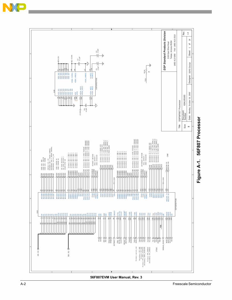
A-1 56F807 Processor . . . . . . . . . . . . . . . . . . . . . . . . . . . . . . . . . . . . . . . . . . . . . . . . . A-2
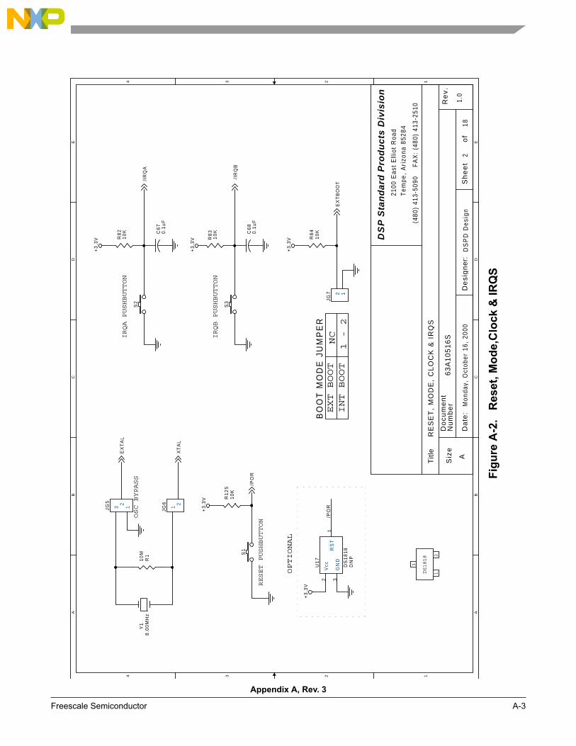
A-2 Reset, Mode,Clock & IRQS. . . . . . . . . . . . . . . . . . . . . . . . . . . . . . . . . . . . . . . . . A-3
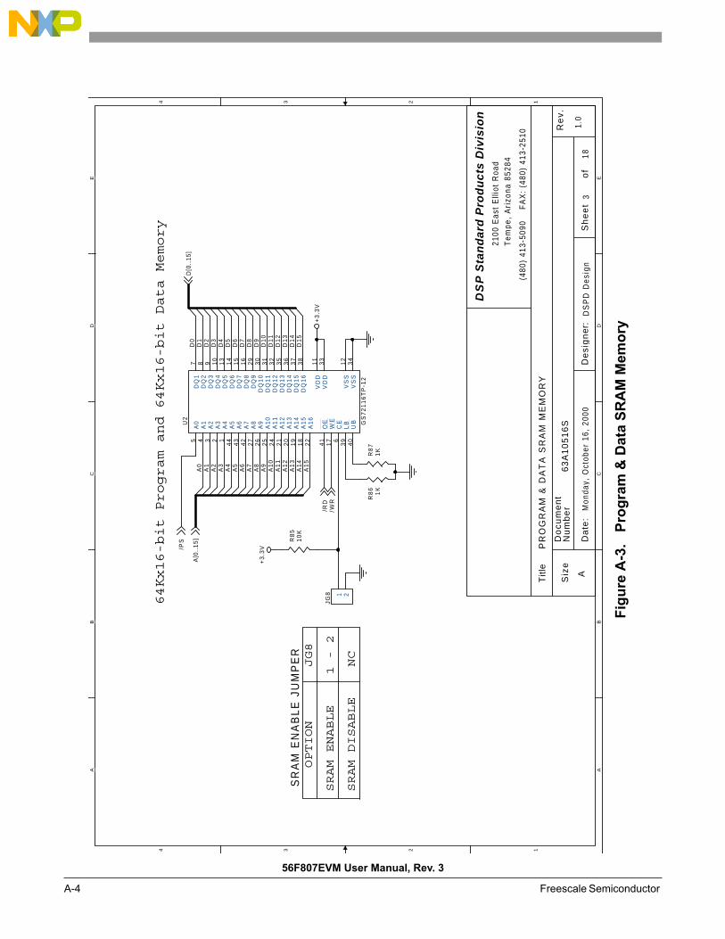
A-3 Program & Data SRAM Memory . . . . . . . . . . . . . . . . . . . . . . . . . . . . . . . . . . . . A-4
A-4 RS-232 and SCI Connectors . . . . . . . . . . . . . . . . . . . . . . . . . . . . . . . . . . . . . . . . A-5
A-5 Debug Serial 4-Channel D/A Converter . . . . . . . . . . . . . . . . . . . . . . . . . . . . . . . A-6
A-6 PWMA and 3 User LEDs. . . . . . . . . . . . . . . . . . . . . . . . . . . . . . . . . . . . . . . . . . . A-7
56F807EVM User Manual, Rev. 3
iv Freescale SemiconductorPreliminary
A-7 Primary UNI-3 Interface and Over-Voltage Fault Detection. . . . . . . . . . . . . . . . A-8
A-8 Secondary UNI-3 and Over-Voltage Detection . . . . . . . . . . . . . . . . . . . . . . . . . . A-9
A-9 User General Purpose Switches and Jumpers . . . . . . . . . . . . . . . . . . . . . . . . . . A-10
A-10 Motor Phase-Current/Back-EMF Voltage Analog Input Selector . . . . . . . . . . . A-11
A-11 Primary and Secondary 3-Phase Over-Current Sense . . . . . . . . . . . . . . . . . . . . A-12
A-12 Primary Zero-Crossing/Quadrature-Encoder or Hall-Effect Selector . . . . . . . . A-13
A-13 Secondary Zero-Crossing/Quadrature-Encoder or Hall-Effect Selector . . . . . . A-14
A-14 Port Expansion Connectors . . . . . . . . . . . . . . . . . . . . . . . . . . . . . . . . . . . . . . . . A-15
A-15 High-Speed CAN Interface . . . . . . . . . . . . . . . . . . . . . . . . . . . . . . . . . . . . . . . . A-16
A-16 Parallel JTAG Host Target Interface and JTAG Connector . . . . . . . . . . . . . . . A-17
A-17 Power Supplies. . . . . . . . . . . . . . . . . . . . . . . . . . . . . . . . . . . . . . . . . . . . . . . . . . A-18
A-18 Bypass Capacitors and Spare Gates . . . . . . . . . . . . . . . . . . . . . . . . . . . . . . . . . . A-19
LIST OF TABLES
List of Tables, Rev. 3
Freescale Semiconductor v
1-1 56F807EVM Default Jumper Options . . . . . . . . . . . . . . . . . . . . . . . . . . . . . . . . . 1-3
2-1 RS-232 Serial Connector Description . . . . . . . . . . . . . . . . . . . . . . . . . . . . . . . . . 2-6
2-2 Operating Mode Selection . . . . . . . . . . . . . . . . . . . . . . . . . . . . . . . . . . . . . . . . . . 2-7
2-3 JTAG Connector Description. . . . . . . . . . . . . . . . . . . . . . . . . . . . . . . . . . . . . . . . 2-9
2-4 Parallel JTAG Interface Disable Jumper Selection . . . . . . . . . . . . . . . . . . . . . . . 2-9
2-5 Parallel JTAG Interface Connector Description . . . . . . . . . . . . . . . . . . . . . . . . 2-10
2-6 Primary UNI-3 Connector Description . . . . . . . . . . . . . . . . . . . . . . . . . . . . . . . 2-14
2-7 Secondary UNI-3 Connector Description . . . . . . . . . . . . . . . . . . . . . . . . . . . . . 2-15
2-8 D/A Header Description. . . . . . . . . . . . . . . . . . . . . . . . . . . . . . . . . . . . . . . . . . . 2-17
2-9 FAULTA1 Source Selection Jumper . . . . . . . . . . . . . . . . . . . . . . . . . . . . . . . . . 2-20
2-10 FAULTB1 Source Selection Jumper . . . . . . . . . . . . . . . . . . . . . . . . . . . . . . . . . 2-22
2-11 CAN Header Description . . . . . . . . . . . . . . . . . . . . . . . . . . . . . . . . . . . . . . . . . . 2-25
2-12 Port B Connector Description . . . . . . . . . . . . . . . . . . . . . . . . . . . . . . . . . . . . . . 2-28
2-13 Port D Connector Description . . . . . . . . . . . . . . . . . . . . . . . . . . . . . . . . . . . . . . 2-28
2-14 Port E Connector Description . . . . . . . . . . . . . . . . . . . . . . . . . . . . . . . . . . . . . . 2-29
2-15 External Memory Control Signal Connector Description . . . . . . . . . . . . . . . . . 2-29
2-16 Timer A Connector Description. . . . . . . . . . . . . . . . . . . . . . . . . . . . . . . . . . . . . 2-30
2-17 Timer B Connector Description. . . . . . . . . . . . . . . . . . . . . . . . . . . . . . . . . . . . . 2-30
2-18 Timer C Connector Description. . . . . . . . . . . . . . . . . . . . . . . . . . . . . . . . . . . . . 2-31
2-19 Timer D Connector Description. . . . . . . . . . . . . . . . . . . . . . . . . . . . . . . . . . . . . 2-31
2-20 External Memory Address Bus Connector Description. . . . . . . . . . . . . . . . . . . 2-32
2-21 External Memory Address Bus Connector Description. . . . . . . . . . . . . . . . . . . 2-33
2-22 A/D Port A Connector Description . . . . . . . . . . . . . . . . . . . . . . . . . . . . . . . . . . 2-33
2-23 A/D Port B Connector Description . . . . . . . . . . . . . . . . . . . . . . . . . . . . . . . . . . 2-34
2-24 SCI0 Connector Description . . . . . . . . . . . . . . . . . . . . . . . . . . . . . . . . . . . . . . . 2-34
2-25 SCI1 Connector Description . . . . . . . . . . . . . . . . . . . . . . . . . . . . . . . . . . . . . . . 2-35
2-26 SPI Connector Description. . . . . . . . . . . . . . . . . . . . . . . . . . . . . . . . . . . . . . . . . 2-35
2-27 CAN Connector Description . . . . . . . . . . . . . . . . . . . . . . . . . . . . . . . . . . . . . . . 2-36

56F807EVM User Manual, Rev. 3
vi Freescale Semiconductor
2-28 PWM Port A Connector Description . . . . . . . . . . . . . . . . . . . . . . . . . . . . . . . . . 2-36
2-29 PWM Port B Connector Description . . . . . . . . . . . . . . . . . . . . . . . . . . . . . . . . . 2-37

Preface, Rev. 3
Freescale Semiconductor vii
Preface
This reference manual describes in detail the hardware on the 56F807 Evaluation Module.
AudienceThis document is intended for application developers who are creating software for
devices using the Freescale 56F807 part.
OrganizationThis manual is organized into two chapters and two appendixes.
• Chapter 1, Introduction - provides an overview of the EVM and its features.
• Chapter 2, Technical Summary - describes in detail the 56F807EVM hardware.
• Appendix A, 56F807EVM Schematics - contains the schematics of the
56F807EVM.
• Appendix B, 56F807EVM Bill of Material - provides a list of the materials used on the
56F807EVM board.
Suggested ReadingMore documentation on the 56F807 and the 56F807EVM kit may be found at URL:
http://www.freescale.com
56F807EVM User Manual, Rev. 3
viii Freescale Semiconductor
Notation ConventionsThis manual uses the following notational conventions:
Term or Value Symbol Examples Exceptions
Active High Signals (Logic One)
No special symbol attached to the signal name
A0CLKO
Active Low Signals(Logic Zero)
Noted with an overbar in text and in most figures
WEOE
In schematic drawings, Active Low Signals may be noted by a backslash: /WE
Hexadecimal Values Begin with a “$” symbol
$0FF0$80
Decimal Values No special symbol attached to the number
1034
Binary Values Begin with the letter “b” attached to the number
b1010b0011
Numbers Considered positive unless specifically noted as a negative value
5-10
Voltage is often shown as positive: +3.3V
Bold Referencesources, paths, emphasis
...see: http://www.freescale.com...

Preface, Rev. 3
Freescale Semiconductor ix
Definitions, Acronyms, and AbbreviationsDefinitions, acronyms and abbreviations for terms used in this document are defined below for
reference.
A/D Analog-to-Digital
CAN Controller Area Network; serial communications peripheral and method
CiA CAN in Automation, an international CAN user’s group that coordinates standards for CAN communications protocols
D/A Digital-to-Analog
EVM Evaluation Module
GPIO General Purpose Input and Output Port
IC Integrated Circuit
JTAG Joint Test Action Group, a bus protocol/interface used for test and debug
LQFP Low-profile Quad Flat Pack
MPIO Multi Purpose Input and Output Port ; shares package pins with other peripherals on the chip and can function as a GPIO
OnCETM
On-Chip Emulation, a debug bus and port created by Freescale to enable designers to create a low-cost hardware interface for a professional-quality debug environment
PCB Printed Circuit Board
PLL Phase Locked Loop
PWM Pulse Width Modulation
RAM Random Access Memory
ROM Read-Only Memory
SCI Serial Communications Interface
SPI Serial Peripheral Interface Port
SRAM Static Random Access Memory
UART Universal Asynchronous Receiver/Transmitter
56F807EVM User Manual, Rev. 3
x Freescale Semiconductor
ReferencesThe following sources were referenced to produce this manual:
[1] DSP56800 Family Manual, DSP56800FM, Freescale Semiconductor
[2] DSP56F801/803/805/807 User’s Manual, DSP56F801-7UM, Freescale Semicon-
ductor
[3] 56F807 Technical Data, DSP56F807, Freescale Semiconductor
[4] CiA Draft Recommendation DR-303-1, Cabling and Connector Pin Assignment,
Version 1.0, CAN in Automation
[5] CAN Specification 2.0B, BOSCH or CAN in Automation

Introduction, Rev. 3
Freescale Semiconductor 1-1
Chapter 1Introduction
The 56F807EVM is used to demonstrate the abilities of the 56F807 and to provide a
hardware tool allowing the development of applications that use the 56F807.
The 56F807EVM is an evaluation module board that includes a 56F807 part, peripheral
expansion connectors, external memory and a CAN interface. The expansion connectors
are for signal monitoring and user feature expandability.
The 56F807EVM is designed for the following purposes:
• Allowing new users to become familiar with the features of the 56800 architecture.
The tools and examples provided with the 56F807EVM facilitate evaluation of the
feature set and the benefits of the family.
• Serving as a platform for real-time software development. The tool suite enables
the user to develop and simulate routines, download the software to on-chip or
on-board RAM, run it, and debug it using a debugger via the JTAG/OnCETM port.
The breakpoint features of the OnCE port enable the user to easily specify complex
break conditions and to execute user-developed software at full-speed, until the
break conditions are satisfied. The ability to examine and modify all user
accessible registers, memory and peripherals through the OnCE port greatly
facilitates the task of the developer.
• Serving as a platform for hardware development. The hardware platform enables
the user to connect external hardware peripherals. The on-board peripherals can be
disabled, providing the user with the ability to reassign any and all of the hybrid
controller’s peripherals. The OnCE port's unobtrusive design means that all of the
memory on the board and on the chip are available to the user.
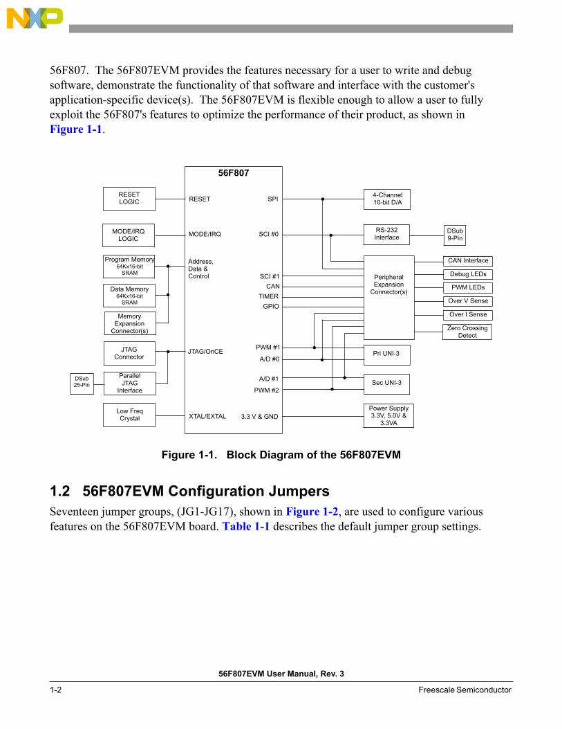
1.1 56F807EVM Architecture
The 56F807EVM facilitates the evaluation of various features present in the 56F807 part
and can be used to develop real-time software and hardware products based on the
56F807EVM User Manual, Rev. 3
1-2 Freescale Semiconductor
56F807. The 56F807EVM provides the features necessary for a user to write and debug
software, demonstrate the functionality of that software and interface with the customer's
application-specific device(s). The 56F807EVM is flexible enough to allow a user to fully
exploit the 56F807's features to optimize the performance of their product, as shown in
Figure 1-1.
56F807
RESET
MODE/IRQ
Address,Data &Control
JTAG/OnCE
XTAL/EXTAL
SPI
SCI #0
SCI #1
CAN
TIMER
GPIO
PWM #1
A/D #0
A/D #1
PWM #2
3.3 V & GND
Peripheral Expansion
Connector(s)
RESETLOGIC
MODE/IRQLOGIC
Program Memory64Kx16-bit
SRAM
MemoryExpansion
Connector(s)
JTAGConnector
ParallelJTAG
Interface
Low FreqCrystal
DSub25-Pin
Data Memory64Kx16-bit
SRAM
DSub9-Pin
CAN Interface
Debug LEDs
PWM LEDs
Over V Sense
Over I Sense
Zero Crossing Detect
Sec UNI-3
Pri UNI-3
RS-232Interface
4-Channel10-bit D/A
Power Supply3.3V, 5.0V &
3.3VA
Figure 1-1. Block Diagram of the 56F807EVM
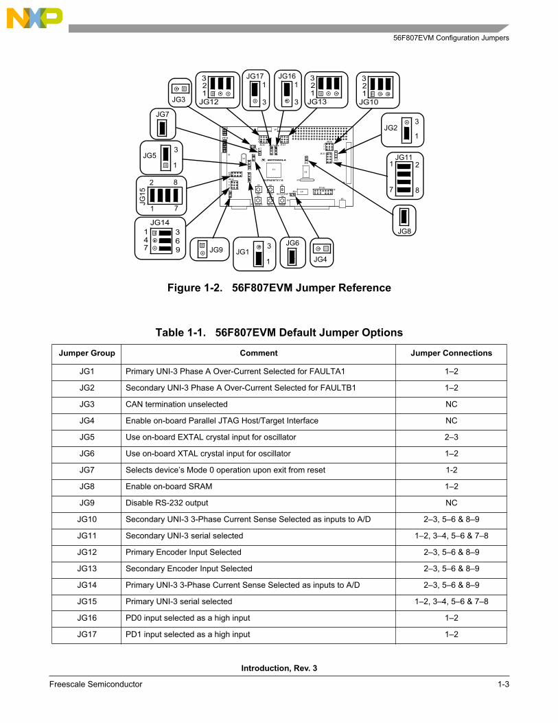
1.2 56F807EVM Configuration Jumpers
Seventeen jumper groups, (JG1-JG17), shown in Figure 1-2, are used to configure various
features on the 56F807EVM board. Table 1-1 describes the default jumper group settings.
JG8
DSP56F807EVM
JG
15
J3JTAG
JG14
1
P3
USER
S/N
LED3
P1
Y1
U1
U2
S2 S3
3
12
JG13
S1
S4 S5 S6
P2
PWM
4
7
JG12
1
32
JG13
1
32
J4 J5
JG17JG16
JG6
JG8
U9
JG11
RESET IRQBIRQA
RUN/STOPGP2GP1
1
2
7
8
JG
15
1 2
7 8
JG11
3
12
JG12
314
JG14
697 JG9
JG2
JG3
JG4
JG6
JG10
1
32
JG4
JG5
JG1
JG9
JG7
J1
J2
1JG16
3
1JG17
3
3
12
JG10
1JG2
3
1
JG13
JG7
JG3
1
JG53
56F807EVM Configuration Jumpers
Introduction, Rev. 3
Freescale Semiconductor 1-3
Figure 1-2. 56F807EVM Jumper Reference
Table 1-1. 56F807EVM Default Jumper Options
Jumper Group Comment Jumper Connections
JG1 Primary UNI-3 Phase A Over-Current Selected for FAULTA1 1–2
JG2 Secondary UNI-3 Phase A Over-Current Selected for FAULTB1 1–2
JG3 CAN termination unselected NC
JG4 Enable on-board Parallel JTAG Host/Target Interface NC
JG5 Use on-board EXTAL crystal input for oscillator 2–3
JG6 Use on-board XTAL crystal input for oscillator 1–2
JG7 Selects device’s Mode 0 operation upon exit from reset 1-2
JG8 Enable on-board SRAM 1–2
JG9 Disable RS-232 output NC
JG10 Secondary UNI-3 3-Phase Current Sense Selected as inputs to A/D 2–3, 5–6 & 8–9
JG11 Secondary UNI-3 serial selected 1–2, 3–4, 5–6 & 7–8
JG12 Primary Encoder Input Selected 2–3, 5–6 & 8–9
JG13 Secondary Encoder Input Selected 2–3, 5–6 & 8–9
JG14 Primary UNI-3 3-Phase Current Sense Selected as inputs to A/D 2–3, 5–6 & 8–9
JG15 Primary UNI-3 serial selected 1–2, 3–4, 5–6 & 7–8
JG16 PD0 input selected as a high input 1–2
JG17 PD1 input selected as a high input 1–2
56F807EVM User Manual, Rev. 3
1-4 Freescale Semiconductor
1.3 56F807EVM Connections
An interconnection diagram is shown in Figure 1-3 for connecting the PC and the external +12V
DC power supply to the 56F807EVM board.
PC-compatible
Cable
Computer
Parallel Extension
56F807EVM
External+12VPower
P1
P2Connect cableto Parallel/Printer port
with 2.1mm,receptacleconnector
Figure 1-3. Connecting the 56F807EVM Cables
. Perform the following steps to connect the 56F807EVM cables:
1. Connect the parallel extension cable to the Parallel port of the host computer
2. Connect the other end of the parallel extension cable to P1, shown in Figure 1-3, on the
56F807EVM board. This provides the connection which allows the host computer to
control the board.
3. Make sure that the external +12V DC, 4.0A power supply is not plugged into a 120V AC
power source
4. Connect the 2.1mm output power plug from the external power supply into P2, shown in
Figure 1-3, on the 56F807EVM board.
5. Apply power to the external power supply. The green Power-On LED, LED10, will
illuminate when power is correctly applied.
Technical Summary, Rev. 3
Freescale Semiconductor 2-1
Chapter 2Technical Summary
The 56F807EVM is designed as a versatile hybrid controller development card for developing
real-time software and hardware products to support a new generation of applications in digital
and wireless messaging, servo and motor control, digital answering machines, feature phones,
modems, and digital cameras. The power of the 16-bit 56F807 controller, combined with the
on-board 64K 16-bit external program static RAM (SRAM), 64K 16-bit external data
SRAM, CAN interface, Hall-Effect/Quadrature Encoder interface, motor zero crossing logic,
motor bus over-current logic, motor bus over-voltage logic and parallel JTAG interface, makes
the 56F807EVM ideal for developing and implementing many motor controlling algorithms, as
well as for learning the architecture and instruction set of the 56F807 processor.
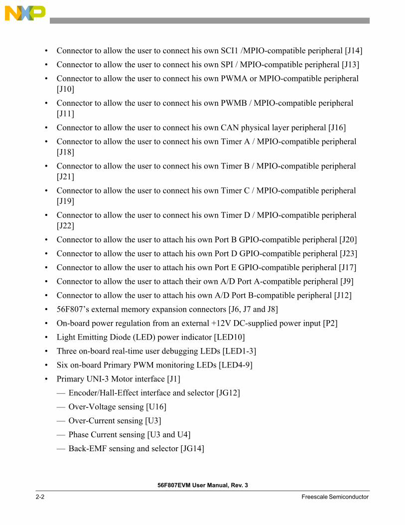
The main features of the 56F807EVM, with board and schematic reference designators, include:
• 56F807 16-bit +3.3V hybrid controller operating at 80MHz [U1]
• External fast static RAM (FSRAM) memory [U2], configured as:
— 64K 16 bits of Program memory with 0 wait states at 70MHz
— 64K 16 bits of Data memory with 0 wait states at 70MHz
• 4-Channel 10-bit Serial D/A, SPI for real-time user data display [U14]
• 8.00MHz crystal oscillator for frequency generation [Y1]
• Optional external oscillator frequency input connector [JG5 and JG6]
• Joint Test Action Group (JTAG) port interface connector for an external debug Host
Target Interface [J3]
• On-board Parallel JTAG Host Target Interface, with a connector for a PC printer port
cable [P1]
• RS-232 interface for easy connection to a host processor [U13 and P3]
• CAN interface for high speed, 1.0Mbps, communications [U8 and J24]
• CAN bypass and bus termination [J25 and JG3]
• Connector to allow the user to connect his own SCI0 / MPIO-compatible peripheral [J15]
56F807EVM User Manual, Rev. 3
2-2 Freescale Semiconductor
• Connector to allow the user to connect his own SCI1 /MPIO-compatible peripheral [J14]
• Connector to allow the user to connect his own SPI / MPIO-compatible peripheral [J13]
• Connector to allow the user to connect his own PWMA or MPIO-compatible peripheral
[J10]
• Connector to allow the user to connect his own PWMB / MPIO-compatible peripheral
[J11]
• Connector to allow the user to connect his own CAN physical layer peripheral [J16]
• Connector to allow the user to connect his own Timer A / MPIO-compatible peripheral
[J18]
• Connector to allow the user to connect his own Timer B / MPIO-compatible peripheral
[J21]
• Connector to allow the user to connect his own Timer C / MPIO-compatible peripheral
[J19]
• Connector to allow the user to connect his own Timer D / MPIO-compatible peripheral
[J22]
• Connector to allow the user to attach his own Port B GPIO-compatible peripheral [J20]
• Connector to allow the user to attach his own Port D GPIO-compatible peripheral [J23]
• Connector to allow the user to attach his own Port E GPIO-compatible peripheral [J17]
• Connector to allow the user to attach their own A/D Port A-compatible peripheral [J9]
• Connector to allow the user to attach his own A/D Port B-compatible peripheral [J12]
• 56F807’s external memory expansion connectors [J6, J7 and J8]
• On-board power regulation from an external +12V DC-supplied power input [P2]
• Light Emitting Diode (LED) power indicator [LED10]
• Three on-board real-time user debugging LEDs [LED1-3]
• Six on-board Primary PWM monitoring LEDs [LED4-9]
• Primary UNI-3 Motor interface [J1]
— Encoder/Hall-Effect interface and selector [JG12]
— Over-Voltage sensing [U16]
— Over-Current sensing [U3]
— Phase Current sensing [U3 and U4]
— Back-EMF sensing and selector [JG14]
56F807
Technical Summary, Rev. 3
Freescale Semiconductor 2-3
— Temperature sensing
— Zero Crossing detection and selector [JG14]
— Pulse Width Modulation
• Secondary UNI-3 Motor interface [J2]
— Encoder/Hall-Effect interface and selector [JG13]
— Over-Voltage sensing [U16]
— Over-Current sensing [U6]
— Phase Current sensing [U5 and U6]
— Back-EMF sensing and selector [JG10]
— Temperature sensing
— Zero Crossing detection and selector [JG10]
— Pulse Width Modulation
• Manual RESET push-button [S1]
• Manual interrupt push-button for IRQA [S2]
• Manual interrupt push-button for IRQB [S3]
• General purpose push-button on GPIO PD3 [S4]
• General purpose push-button on GPIO PD4 [S5]
• General purpose toggle switch for RUN/STOP control(PD5) [S6]
• General purpose jumper on GPIO PD0 [JG16]
• General purpose jumper on GPIO PD1 [JG17]
2.1 56F807
The 56F807EVM uses a Freescale DSP56F807FV80 part, designated as U1 on the board and in
the schematics. This part will operate at a maximum speed of 80MHz. A full description of the
56F807, including functionality and user information, is provided in these documents:
• DSP56800 Family Manual, (DSP56800FM): Provides a detailed description of the core
processor, including internal status and control registers and a detailed description of the
family instruction set.
• DSP56F801/803/805/807 User’s Manual, (DSP56F801-7UM): Provides an overview
description of the hybrid controller and detailed information about the on-chip

56F807EVM User Manual, Rev. 3
2-4 Freescale Semiconductor
components including the memory and I/O maps, peripheral functionality, and
control/status register descriptions for each subsystem.
• 56F807 Technical Data, (DSP56F807): Provides features list and specifications including
signal descriptions, DC power requirements, AC timing requirements and available
packaging.
Refer to these documents for detailed information about chip functionality and operation. They
can be found on this URL:
http://www.freescale.com
Program and Data Memory
Technical Summary, Rev. 3
Freescale Semiconductor 2-5
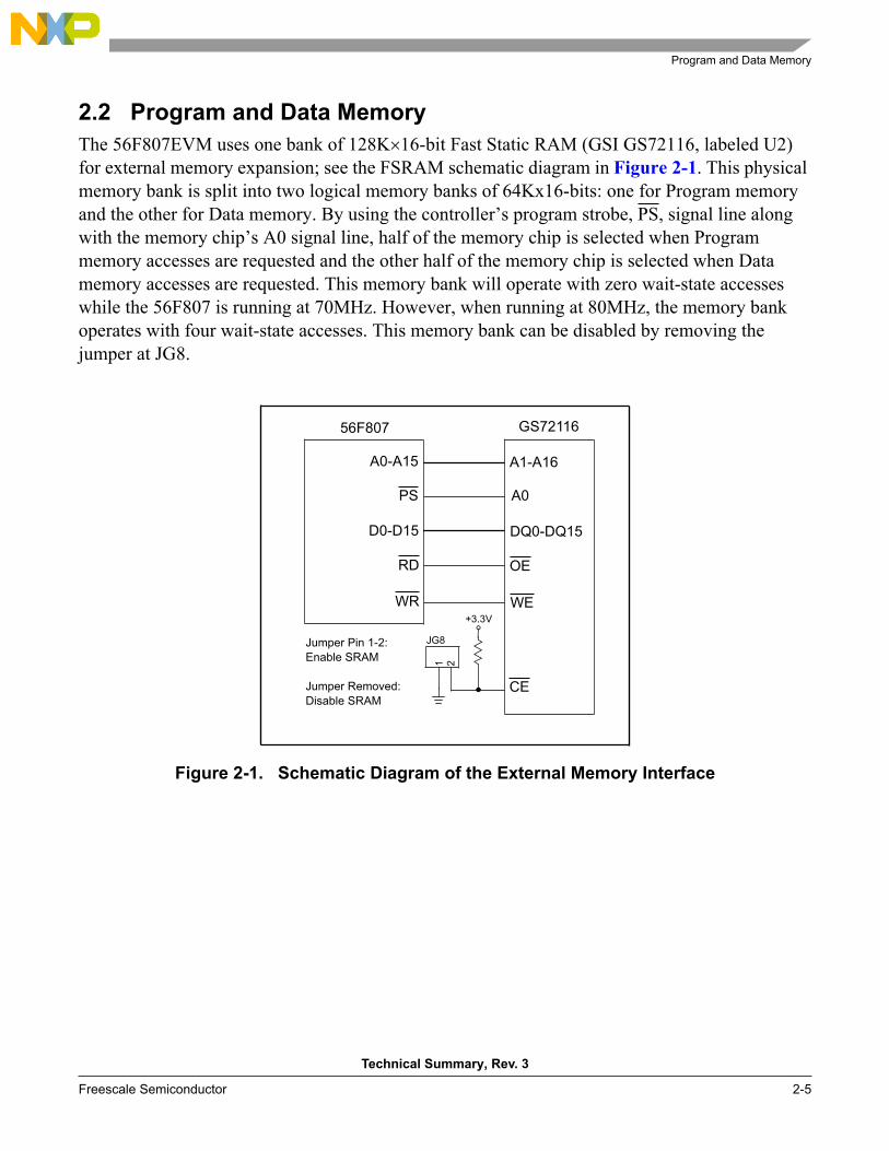
2.2 Program and Data Memory
The 56F807EVM uses one bank of 128K 16-bit Fast Static RAM (GSI GS72116, labeled U2)
for external memory expansion; see the FSRAM schematic diagram in Figure 2-1. This physical
memory bank is split into two logical memory banks of 64Kx16-bits: one for Program memory
and the other for Data memory. By using the controller’s program strobe, PS, signal line along
with the memory chip’s A0 signal line, half of the memory chip is selected when Program
memory accesses are requested and the other half of the memory chip is selected when Data
memory accesses are requested. This memory bank will operate with zero wait-state accesses
while the 56F807 is running at 70MHz. However, when running at 80MHz, the memory bank
operates with four wait-state accesses. This memory bank can be disabled by removing the
jumper at JG8.
56F807 GS72116
A0-A15
PS
D0-D15
RD
WR
A1-A16
A0
DQ0-DQ15
OE
WE
CE
1 2
JG8
+3.3V
Jumper Pin 1-2:
Enable SRAM
Jumper Removed:
Disable SRAM
Figure 2-1. Schematic Diagram of the External Memory Interface
56F807EVM User Manual, Rev. 3
2-6 Freescale Semiconductor
2.3 RS-232 Serial Communications
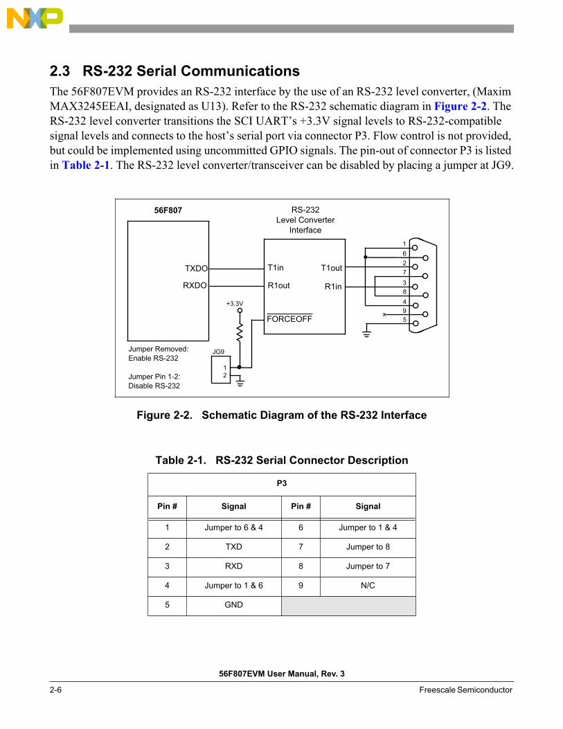
The 56F807EVM provides an RS-232 interface by the use of an RS-232 level converter, (Maxim
MAX3245EEAI, designated as U13). Refer to the RS-232 schematic diagram in Figure 2-2. The
RS-232 level converter transitions the SCI UART’s +3.3V signal levels to RS-232-compatible
signal levels and connects to the host’s serial port via connector P3. Flow control is not provided,
but could be implemented using uncommitted GPIO signals. The pin-out of connector P3 is listed
in Table 2-1. The RS-232 level converter/transceiver can be disabled by placing a jumper at JG9.
56F807 RS-232Level Converter
Interface
TXDO
RXDO R1in
T1outT1in
R1out
FORCEOFF
JG9
12
6
3
2
7
8
4
5x
1
9+3.3V
Jumper Removed:
Enable RS-232
Jumper Pin 1-2:
Disable RS-232
Figure 2-2. Schematic Diagram of the RS-232 Interface
Table 2-1. RS-232 Serial Connector Description
P3
Pin # Signal Pin # Signal
1 Jumper to 6 & 4 6 Jumper to 1 & 4
2 TXD 7 Jumper to 8
3 RXD 8 Jumper to 7
4 Jumper to 1 & 6 9 N/C
5 GND
Operating Mode
Technical Summary, Rev. 3
Freescale Semiconductor 2-7
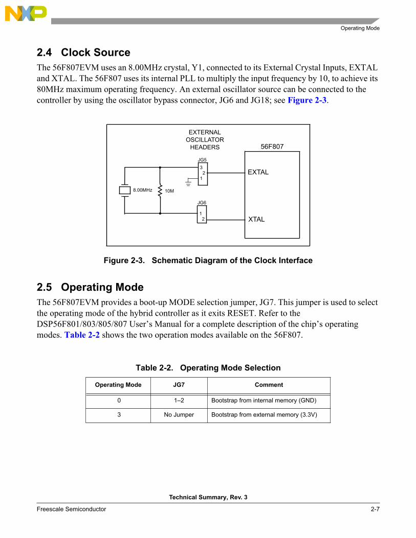
2.4 Clock Source
The 56F807EVM uses an 8.00MHz crystal, Y1, connected to its External Crystal Inputs, EXTAL
and XTAL. The 56F807 uses its internal PLL to multiply the input frequency by 10, to achieve its
80MHz maximum operating frequency. An external oscillator source can be connected to the
controller by using the oscillator bypass connector, JG6 and JG18; see Figure 2-3.
56F807
EXTERNALOSCILLATOR
HEADERS
JG5
3 21
1 2
EXTAL
XTAL
JG6
10M8.00MHz
Figure 2-3. Schematic Diagram of the Clock Interface
2.5 Operating Mode
The 56F807EVM provides a boot-up MODE selection jumper, JG7. This jumper is used to select
the operating mode of the hybrid controller as it exits RESET. Refer to the
DSP56F801/803/805/807 User’s Manual for a complete description of the chip’s operating
modes. Table 2-2 shows the two operation modes available on the 56F807.
Table 2-2. Operating Mode Selection
Operating Mode JG7 Comment
0 1–2 Bootstrap from internal memory (GND)
3 No Jumper Bootstrap from external memory (3.3V)
56F807EVM User Manual, Rev. 3
2-8 Freescale Semiconductor
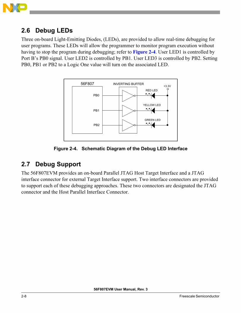
2.6 Debug LEDs
Three on-board Light-Emitting Diodes, (LEDs), are provided to allow real-time debugging for
user programs. These LEDs will allow the programmer to monitor program execution without
having to stop the program during debugging; refer to Figure 2-4. User LED1 is controlled by
Port B’s PB0 signal. User LED2 is controlled by PB1. User LED3 is controlled by PB2. Setting
PB0, PB1 or PB2 to a Logic One value will turn on the associated LED.
56F807 INVERTING BUFFER
PB0
PB1
PB2
GREEN LED
YELLOW LED
RED LED
+3.3V
Figure 2-4. Schematic Diagram of the Debug LED Interface
2.7 Debug Support
The 56F807EVM provides an on-board Parallel JTAG Host Target Interface and a JTAG
interface connector for external Target Interface support. Two interface connectors are provided
to support each of these debugging approaches. These two connectors are designated the JTAG
connector and the Host Parallel Interface Connector.
Debug Support
Technical Summary, Rev. 3
Freescale Semiconductor 2-9
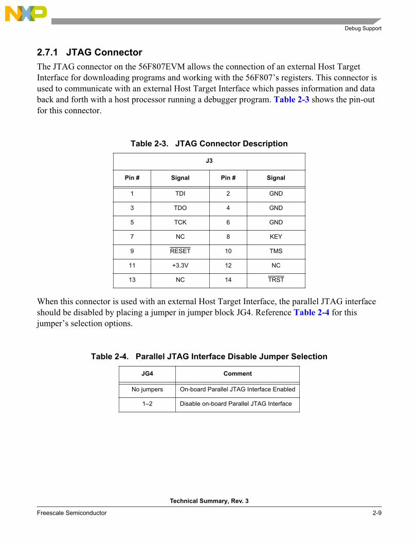
2.7.1 JTAG Connector
The JTAG connector on the 56F807EVM allows the connection of an external Host Target
Interface for downloading programs and working with the 56F807’s registers. This connector is
used to communicate with an external Host Target Interface which passes information and data
back and forth with a host processor running a debugger program. Table 2-3 shows the pin-out
for this connector.
Table 2-3. JTAG Connector Description
J3
Pin # Signal Pin # Signal
1 TDI 2 GND
3 TDO 4 GND
5 TCK 6 GND
7 NC 8 KEY
9 RESET 10 TMS
11 +3.3V 12 NC
13 NC 14 TRST
When this connector is used with an external Host Target Interface, the parallel JTAG interface
should be disabled by placing a jumper in jumper block JG4. Reference Table 2-4 for this
jumper’s selection options.
Table 2-4. Parallel JTAG Interface Disable Jumper Selection
JG4 Comment
No jumpers On-board Parallel JTAG Interface Enabled
1–2 Disable on-board Parallel JTAG Interface
56F807EVM User Manual, Rev. 3
2-10 Freescale Semiconductor
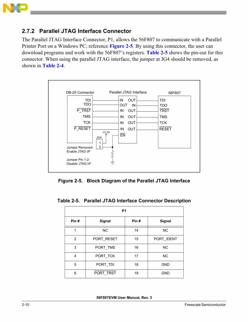
2.7.2 Parallel JTAG Interface Connector
The Parallel JTAG Interface Connector, P1, allows the 56F807 to communicate with a Parallel
Printer Port on a Windows PC; reference Figure 2-5. By using this connector, the user can
download programs and work with the 56F807’s registers. Table 2-5 shows the pin-out for this
connector. When using the parallel JTAG interface, the jumper at JG4 should be removed, as
shown in Table 2-4.
DB-25 Connector Parallel JTAG Interface 56F807
TDITDO
P_TRST
TMS
TCK
P_RESET
OUT
OUT
OUT
OUT
OUT
OUTIN
IN
IN
IN
IN
IN
EN
TDI
TDO
TRST
TMS
TCK
RESET
JG4
1
2
+3.3V
Jumper Removed:
Enable JTAG I/F
Jumper Pin 1-2:
Disable JTAG I/F
Figure 2-5. Block Diagram of the Parallel JTAG Interface
Table 2-5. Parallel JTAG Interface Connector Description
P1
Pin # Signal Pin # Signal
1 NC 14 NC
2 PORT_RESET 15 PORT_IDENT
3 PORT_TMS 16 NC
4 PORT_TCK 17 NC
5 PORT_TDI 18 GND
6 PORT_TRST 19 GND
External Interrupts
Technical Summary, Rev. 3
Freescale Semiconductor 2-11
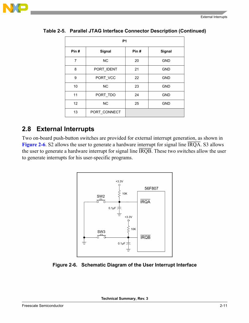
2.8 External Interrupts
Two on-board push-button switches are provided for external interrupt generation, as shown in
Figure 2-6. S2 allows the user to generate a hardware interrupt for signal line IRQA. S3 allows
the user to generate a hardware interrupt for signal line IRQB. These two switches allow the user
to generate interrupts for his user-specific programs.
56F807
IRQA
IRQB
+3.3V
+3.3V
10K
10K
SW2
SW3
0.1µF
0.1µF
Figure 2-6. Schematic Diagram of the User Interrupt Interface
7 NC 20 GND
8 PORT_IDENT 21 GND
9 PORT_VCC 22 GND
10 NC 23 GND
11 PORT_TDO 24 GND
12 NC 25 GND
13 PORT_CONNECT
Table 2-5. Parallel JTAG Interface Connector Description (Continued)
P1
Pin # Signal Pin # Signal
56F807EVM User Manual, Rev. 3
2-12 Freescale Semiconductor
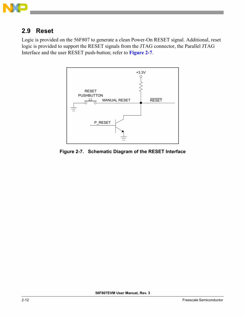
2.9 Reset
Logic is provided on the 56F807 to generate a clean Power-On RESET signal. Additional, reset
logic is provided to support the RESET signals from the JTAG connector, the Parallel JTAG
Interface and the user RESET push-button; refer to Figure 2-7.
RESETPUSHBUTTON
MANUAL RESET
P_RESET
RESET
+3.3V
Figure 2-7. Schematic Diagram of the RESET Interface
Power Supply
Technical Summary, Rev. 3
Freescale Semiconductor 2-13
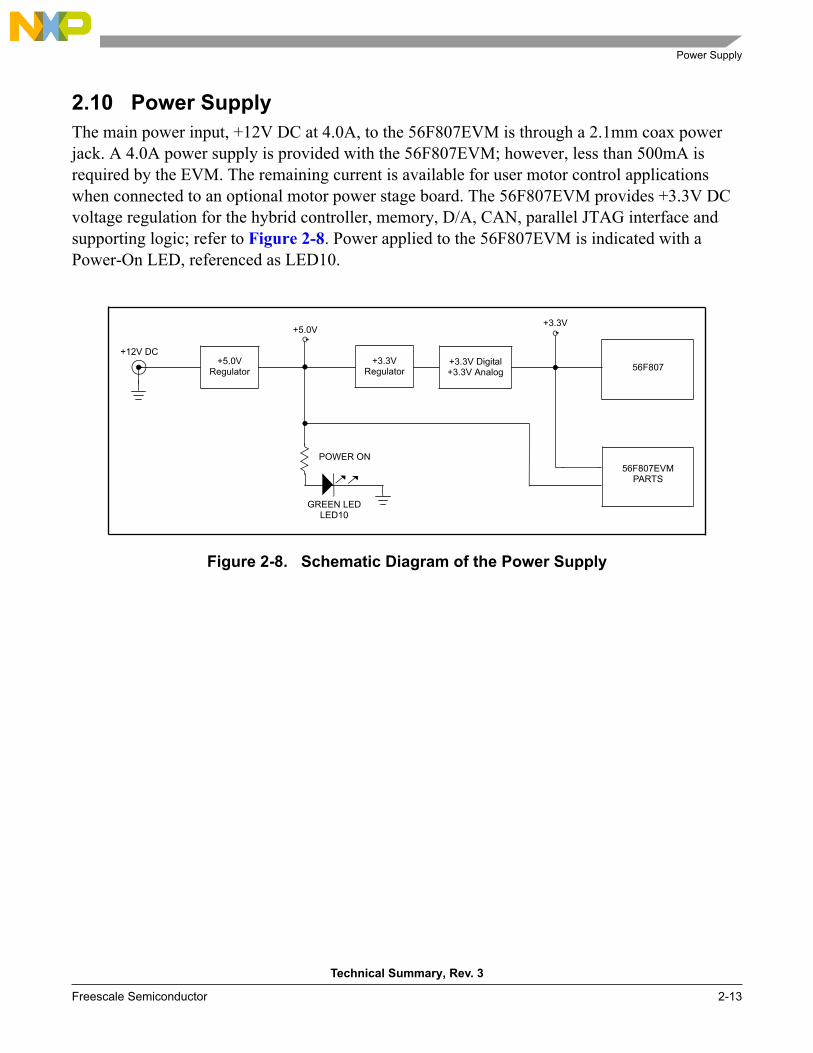
2.10 Power Supply
The main power input, +12V DC at 4.0A, to the 56F807EVM is through a 2.1mm coax power
jack. A 4.0A power supply is provided with the 56F807EVM; however, less than 500mA is
required by the EVM. The remaining current is available for user motor control applications
when connected to an optional motor power stage board. The 56F807EVM provides +3.3V DC
voltage regulation for the hybrid controller, memory, D/A, CAN, parallel JTAG interface and
supporting logic; refer to Figure 2-8. Power applied to the 56F807EVM is indicated with a
Power-On LED, referenced as LED10.
+12V DC+5.0V
Regulator
POWER ON
GREEN LEDLED10
+3.3VRegulator
+3.3V Digital+3.3V Analog
+5.0V+3.3V
56F807
56F807EVMPARTS
Figure 2-8. Schematic Diagram of the Power Supply
56F807EVM User Manual, Rev. 3
2-14 Freescale Semiconductor
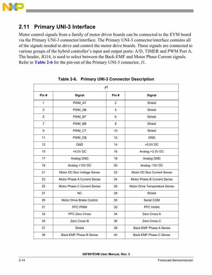
2.11 Primary UNI-3 Interface
Motor control signals from a family of motor driver boards can be connected to the EVM board
via the Primary UNI-3 connector/interface. The Primary UNI-3 connector/interface contains all
of the signals needed to drive and control the motor drive boards. These signals are connected to
various groups of the hybrid controller’s input and output ports: A/D, TIMER and PWM Port A.
The header, JG14, is used to select between the Back-EMF and Motor Phase Current signals.
Refer to Table 2-6 for the pin-out of the Primary UNI-3 connector, J1.
Table 2-6. Primary UNI-3 Connector Description
J1
Pin # Signal Pin # Signal
1 PWM_AT 2 Shield
3 PWM_AB 4 Shield
5 PWM_BT 6 Shield
7 PWM_BB 8 Shield
9 PWM_CT 10 Shield
11 PWM_CB 12 GND
13 GND 14 +5.0V DC
15 +5.0V DC 16 Analog +3.3V DC
17 Analog GND 18 Analog GND
19 Analog +15V DC 20 Analog -15V DC
21 Motor DC Bus Voltage Sense 22 Motor DC Bus Current Sense
23 Motor Phase A Current Sense 24 Motor Phase B Current Sense
25 Motor Phase C Current Sense 26 Motor Drive Temperature Sense
27 NC 28 Shield
29 Motor Drive Brake Control 30 Serial COM
31 PFC PWM 32 PFC Inhibit
33 PFC Zero Cross 34 Zero Cross A
35 Zero Cross B 36 Zero Cross C
37 Shield 38 Back-EMF Phase A Sense
39 Back-EMF Phase B Sense 40 Back-EMF Phase C Sense
Secondary UNI-3 Interface
Technical Summary, Rev. 3
Freescale Semiconductor 2-15
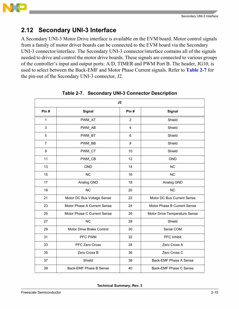
2.12 Secondary UNI-3 Interface
A Secondary UNI-3 Motor Drive interface is available on the EVM board. Motor control signals
from a family of motor driver boards can be connected to the EVM board via the Secondary
UNI-3 connector/interface. The Secondary UNI-3 connector/interface contains all of the signals
needed to drive and control the motor drive boards. These signals are connected to various groups
of the controller’s input and output ports: A/D, TIMER and PWM Port B. The header, JG10, is
used to select between the Back-EMF and Motor Phase Current signals. Refer to Table 2-7 for
the pin-out of the Secondary UNI-3 connector, J2.
Table 2-7. Secondary UNI-3 Connector Description
J2
Pin # Signal Pin # Signal
1 PWM_AT 2 Shield
3 PWM_AB 4 Shield
5 PWM_BT 6 Shield
7 PWM_BB 8 Shield
9 PWM_CT 10 Shield
11 PWM_CB 12 GND
13 GND 14 NC
15 NC 16 NC
17 Analog GND 18 Analog GND
19 NC 20 NC
21 Motor DC Bus Voltage Sense 22 Motor DC Bus Current Sense
23 Motor Phase A Current Sense 24 Motor Phase B Current Sense
25 Motor Phase C Current Sense 26 Motor Drive Temperature Sense
27 NC 28 Shield
29 Motor Drive Brake Control 30 Serial COM
31 PFC PWM 32 PFC Inhibit
33 PFC Zero Cross 34 Zero Cross A
35 Zero Cross B 36 Zero Cross C
37 Shield 38 Back-EMF Phase A Sense
39 Back-EMF Phase B Sense 40 Back-EMF Phase C Sense
56F807EVM User Manual, Rev. 3
2-16 Freescale Semiconductor
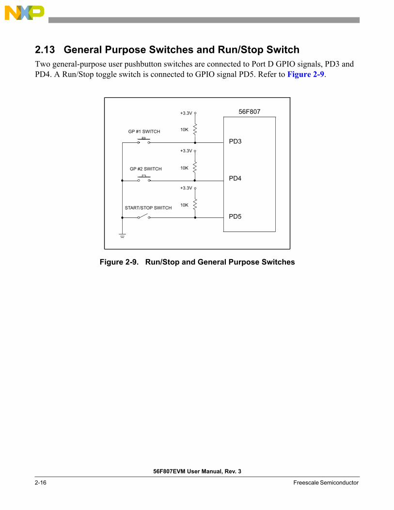
2.13 General Purpose Switches and Run/Stop Switch
Two general-purpose user pushbutton switches are connected to Port D GPIO signals, PD3 and
PD4. A Run/Stop toggle switch is connected to GPIO signal PD5. Refer to Figure 2-9.
56F807+3.3V
PD3
PD4
PD5
+3.3V
10K
10K
10K
GP #1 SWITCH
GP #2 SWITCH
START/STOP SWITCH
+3.3V
Figure 2-9. Run/Stop and General Purpose Switches
Serial 10-bit 4-channel D/A Converter
Technical Summary, Rev. 3
Freescale Semiconductor 2-17
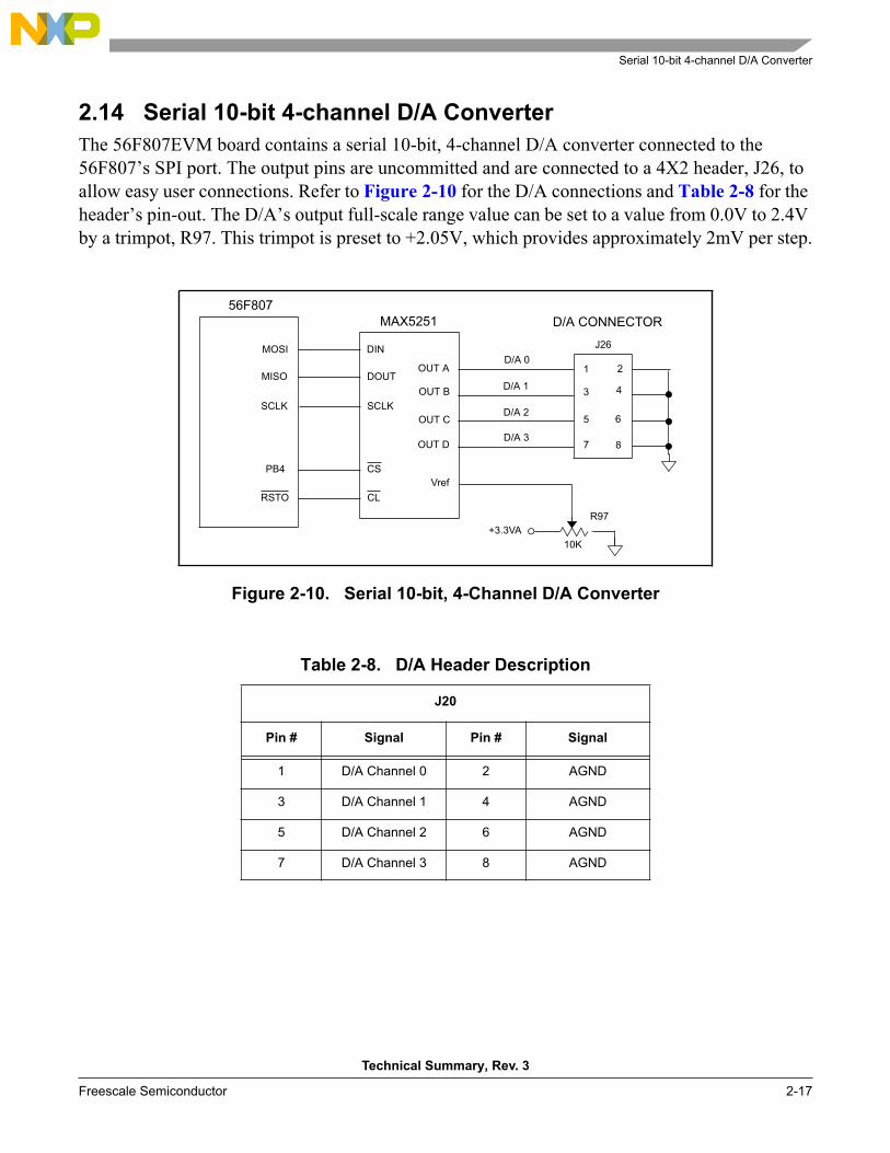
2.14 Serial 10-bit 4-channel D/A Converter
The 56F807EVM board contains a serial 10-bit, 4-channel D/A converter connected to the
56F807’s SPI port. The output pins are uncommitted and are connected to a 4X2 header, J26, to
allow easy user connections. Refer to Figure 2-10 for the D/A connections and Table 2-8 for the
header’s pin-out. The D/A’s output full-scale range value can be set to a value from 0.0V to 2.4V
by a trimpot, R97. This trimpot is preset to +2.05V, which provides approximately 2mV per step.
56F807MAX5251 D/A CONNECTOR
MOSI
MISO
SCLK
PB4
RSTO
DIN
DOUT
SCLK
CS
CL
OUT A
OUT B
OUT C
OUT D
Vref
1
3
5
7
2
4
6
8
D/A 0
D/A 1
D/A 2
D/A 3
J26
+3.3VA
10K
R97
Figure 2-10. Serial 10-bit, 4-Channel D/A Converter
Table 2-8. D/A Header Description
J20
Pin # Signal Pin # Signal
1 D/A Channel 0 2 AGND
3 D/A Channel 1 4 AGND
5 D/A Channel 2 6 AGND
7 D/A Channel 3 8 AGND
56F807EVM User Manual, Rev. 3
2-18 Freescale Semiconductor
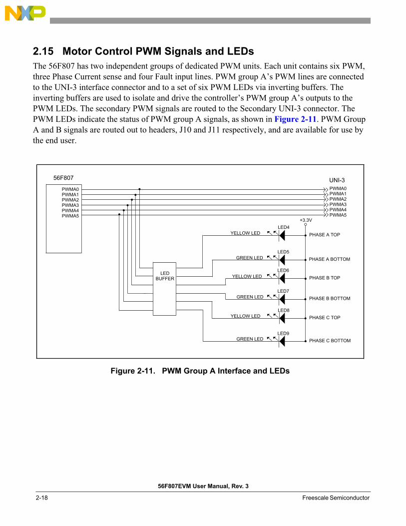
2.15 Motor Control PWM Signals and LEDs
The 56F807 has two independent groups of dedicated PWM units. Each unit contains six PWM,
three Phase Current sense and four Fault input lines. PWM group A’s PWM lines are connected
to the UNI-3 interface connector and to a set of six PWM LEDs via inverting buffers. The
inverting buffers are used to isolate and drive the controller’s PWM group A’s outputs to the
PWM LEDs. The secondary PWM signals are routed to the Secondary UNI-3 connector. The
PWM LEDs indicate the status of PWM group A signals, as shown in Figure 2-11. PWM Group
A and B signals are routed out to headers, J10 and J11 respectively, and are available for use by
the end user.
56F807
LEDBUFFER
UNI-3
PWMA0PWMA1PWMA2PWMA3PWMA4PWMA5
PWMA0PWMA1PWMA2PWMA3PWMA4PWMA5
YELLOW LED
GREEN LED
GREEN LED
GREEN LED
YELLOW LED
YELLOW LED
+3.3V
PHASE A TOP
PHASE A BOTTOM
PHASE B TOP
PHASE B BOTTOM
PHASE C TOP
PHASE C BOTTOM
LED4
LED5
LED6
LED7
LED8
LED9
Figure 2-11. PWM Group A Interface and LEDs
Motor Protection Logic
Technical Summary, Rev. 3
Freescale Semiconductor 2-19
2.16 Motor Protection Logic
The 56F807EVM contains two UNI-3 connectors that interface with various motor drive boards,
Primary UNI-3 and Secondary UNI-3. The device can sense error conditions generated by the
motor power stage boards via signals on the UNI-3 connector. The motor driver board’s Motor
Supply DC Bus Voltage, Current and Motor Phase Currents are sensed on the power stage board.
The conditioned signals are transferred to the board via the UNI-3 connector. These analog input
signals are compared to a limit set by trimpots. If the input analog signals are greater than the
limit set by the trimpot, a controller digital voltage-compatible +3.3V DC fault signal is
generated.
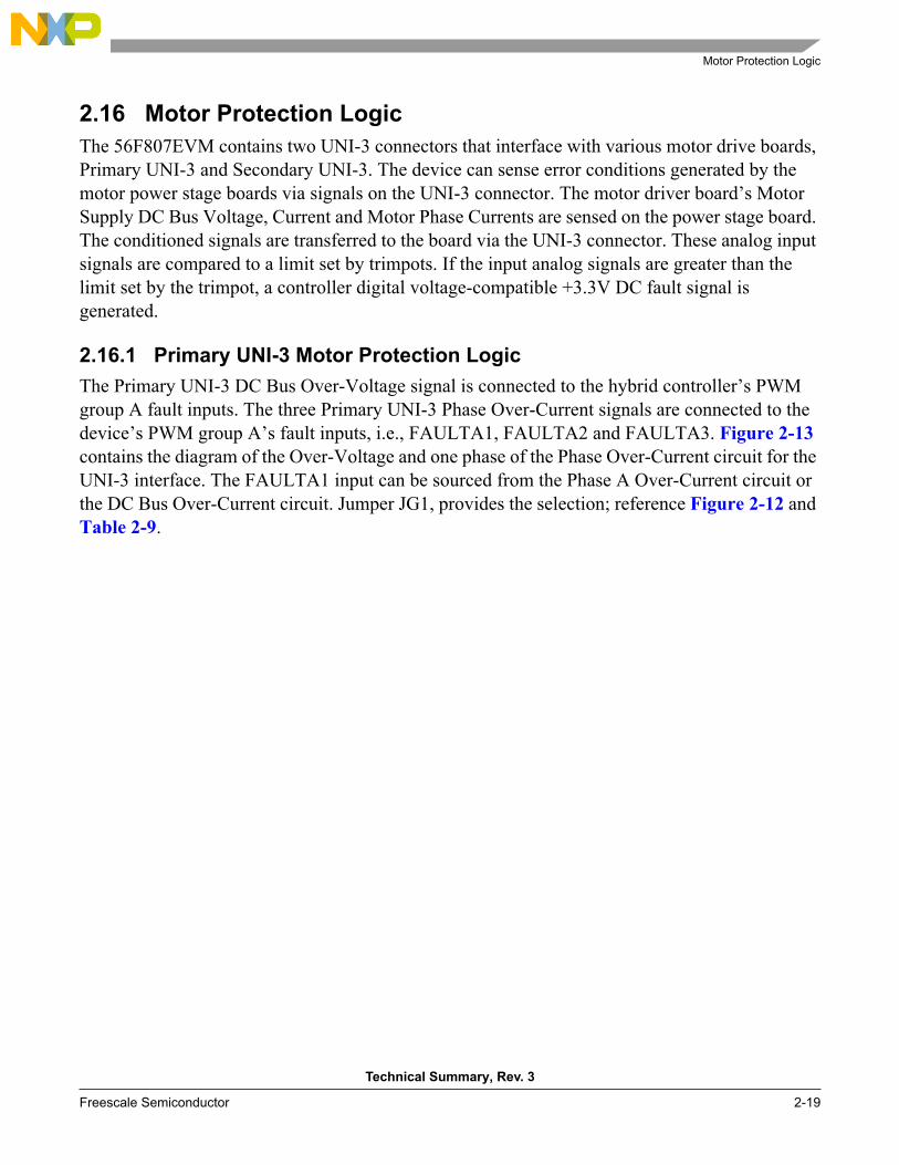
2.16.1 Primary UNI-3 Motor Protection Logic
The Primary UNI-3 DC Bus Over-Voltage signal is connected to the hybrid controller’s PWM
group A fault inputs. The three Primary UNI-3 Phase Over-Current signals are connected to the
device’s PWM group A’s fault inputs, i.e., FAULTA1, FAULTA2 and FAULTA3. Figure 2-13
contains the diagram of the Over-Voltage and one phase of the Phase Over-Current circuit for the
UNI-3 interface. The FAULTA1 input can be sourced from the Phase A Over-Current circuit or
the DC Bus Over-Current circuit. Jumper JG1, provides the selection; reference Figure 2-12 and
Table 2-9.
DC BUS CURRENT SENSE
I_sense_DCB
+
–
+5.0V
+5.0V
LM393
+3.3V
JG1
3 21
FAULTA1
+
–
+5.0V
+5.0V
+3.3V
PHA_IS
PHASE A CURRENT SENSE
LM393
56F807EVM User Manual, Rev. 3
2-20 Freescale Semiconductor
Figure 2-12. FAULTA1 Selection Circuit
Table 2-9. FAULTA1 Source Selection Jumper
JG1 Comment
1–2 Phase A Over-Current Sense input
2–3 DC Bus Over-Current Sense input
Motor Protection Logic
Technical Summary, Rev. 3
Freescale Semiconductor 2-21
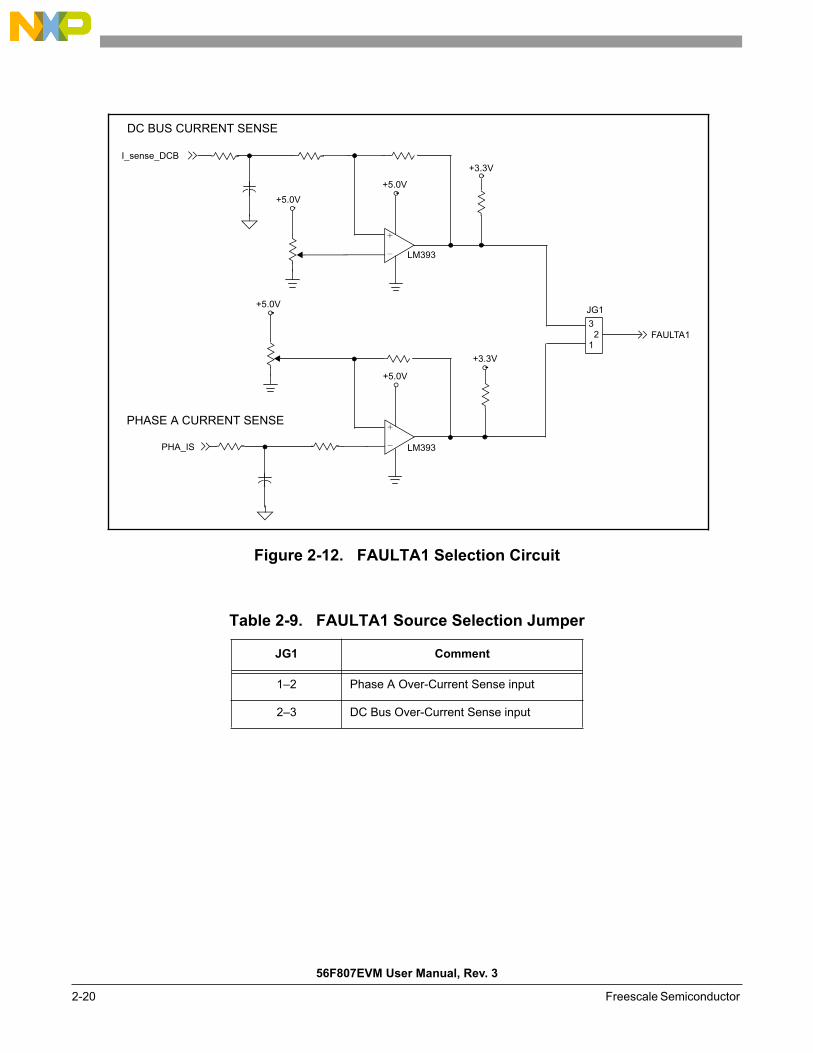
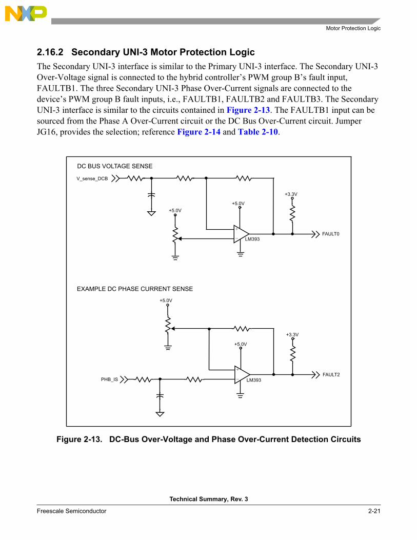
2.16.2 Secondary UNI-3 Motor Protection Logic
The Secondary UNI-3 interface is similar to the Primary UNI-3 interface. The Secondary UNI-3
Over-Voltage signal is connected to the hybrid controller’s PWM group B’s fault input,
FAULTB1. The three Secondary UNI-3 Phase Over-Current signals are connected to the
device’s PWM group B fault inputs, i.e., FAULTB1, FAULTB2 and FAULTB3. The Secondary
UNI-3 interface is similar to the circuits contained in Figure 2-13. The FAULTB1 input can be
sourced from the Phase A Over-Current circuit or the DC Bus Over-Current circuit. Jumper
JG16, provides the selection; reference Figure 2-14 and Table 2-10.
+5.0V
+
–
+5.0V
+3.3V
V_sense_DCB
FAULT0LM393
+
–
+5.0V
+5.0V
+3.3V
FAULT2PHB_IS LM393
DC BUS VOLTAGE SENSE
EXAMPLE DC PHASE CURRENT SENSE
Figure 2-13. DC-Bus Over-Voltage and Phase Over-Current Detection Circuits
1
2
3
I_sense_DCB
+5.0V
+5.0V
+3.3V
DC BUS CURRENT SENSE
LM393
+
-
+
-
+5.0V
+5.0V
+3.3V
FAULTB1
JG2
PHASE A CURRENT SENSE
PHA_ISLM393
56F807EVM User Manual, Rev. 3
2-22 Freescale Semiconductor
Figure 2-14. FAULTB1 Selection Circuit
Table 2-10. FAULTB1 Source Selection Jumper
JG2 Comment
1–2 Phase A Over-Current Sense input
2–3 DC Bus Over-Current Sense input
Quadrature Encoder/Hall-Effect Interface
Technical Summary, Rev. 3
Freescale Semiconductor 2-23
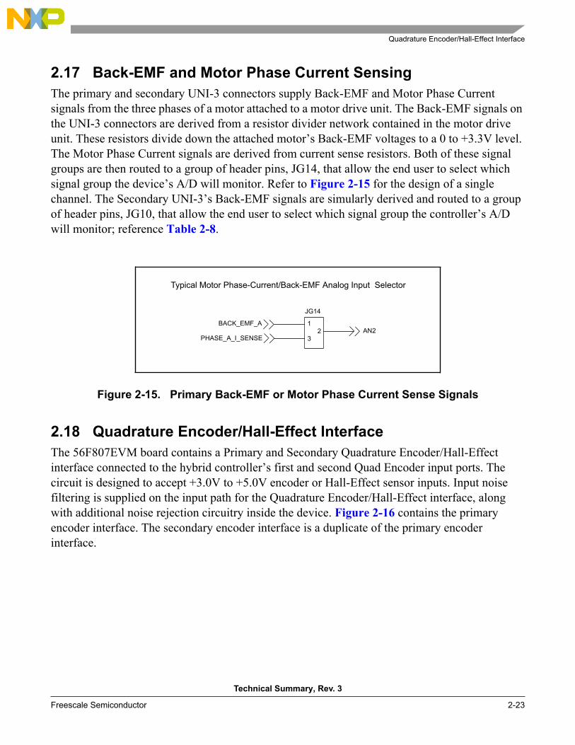
2.17 Back-EMF and Motor Phase Current Sensing
The primary and secondary UNI-3 connectors supply Back-EMF and Motor Phase Current
signals from the three phases of a motor attached to a motor drive unit. The Back-EMF signals on
the UNI-3 connectors are derived from a resistor divider network contained in the motor drive
unit. These resistors divide down the attached motor’s Back-EMF voltages to a 0 to +3.3V level.
The Motor Phase Current signals are derived from current sense resistors. Both of these signal
groups are then routed to a group of header pins, JG14, that allow the end user to select which
signal group the device’s A/D will monitor. Refer to Figure 2-15 for the design of a single
channel. The Secondary UNI-3’s Back-EMF signals are simularly derived and routed to a group
of header pins, JG10, that allow the end user to select which signal group the controller’s A/D
will monitor; reference Table 2-8.
Typical Motor Phase-Current/Back-EMF Analog Input Selector
BACK_EMF_A
PHASE_A_I_SENSE
1 23
AN2
JG14
Figure 2-15. Primary Back-EMF or Motor Phase Current Sense Signals
2.18 Quadrature Encoder/Hall-Effect Interface
The 56F807EVM board contains a Primary and Secondary Quadrature Encoder/Hall-Effect
interface connected to the hybrid controller’s first and second Quad Encoder input ports. The
circuit is designed to accept +3.0V to +5.0V encoder or Hall-Effect sensor inputs. Input noise
filtering is supplied on the input path for the Quadrature Encoder/Hall-Effect interface, along
with additional noise rejection circuitry inside the device. Figure 2-16 contains the primary
encoder interface. The secondary encoder interface is a duplicate of the primary encoder
interface.
56F807EVM User Manual, Rev. 3
2-24 Freescale Semiconductor
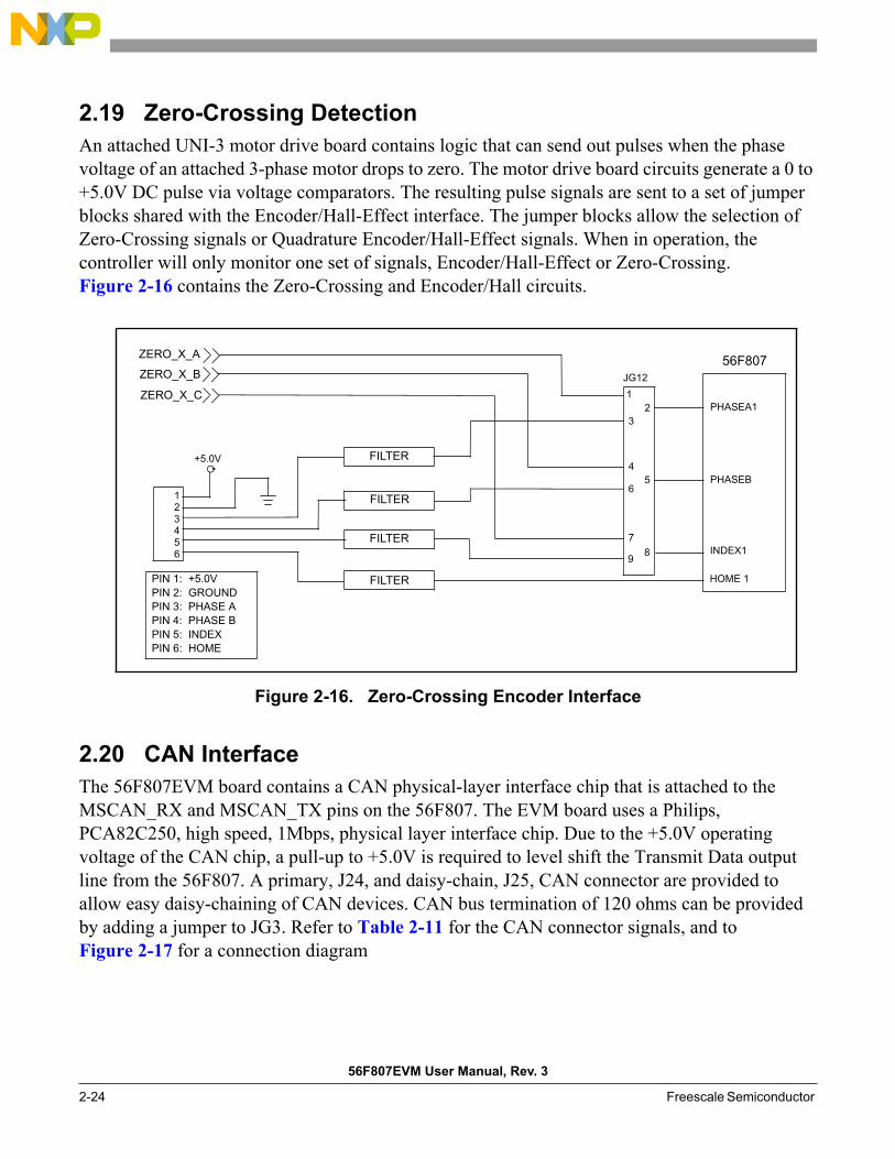
2.19 Zero-Crossing Detection
An attached UNI-3 motor drive board contains logic that can send out pulses when the phase
voltage of an attached 3-phase motor drops to zero. The motor drive board circuits generate a 0 to
+5.0V DC pulse via voltage comparators. The resulting pulse signals are sent to a set of jumper
blocks shared with the Encoder/Hall-Effect interface. The jumper blocks allow the selection of
Zero-Crossing signals or Quadrature Encoder/Hall-Effect signals. When in operation, the
controller will only monitor one set of signals, Encoder/Hall-Effect or Zero-Crossing.
Figure 2-16 contains the Zero-Crossing and Encoder/Hall circuits.
ZERO_X_A
ZERO_X_B
ZERO_X_C
123456
+5.0V FILTER
FILTER
FILTER
FILTERPIN 1: +5.0V
PIN 2: GROUND
PIN 3: PHASE A
PIN 4: PHASE B
PIN 5: INDEX
PIN 6: HOME
1
2
3
4
56
7
89
JG12
56F807
PHASEA1
PHASEB
INDEX1
HOME 1
Figure 2-16. Zero-Crossing Encoder Interface
2.20 CAN Interface
The 56F807EVM board contains a CAN physical-layer interface chip that is attached to the
MSCAN_RX and MSCAN_TX pins on the 56F807. The EVM board uses a Philips,
PCA82C250, high speed, 1Mbps, physical layer interface chip. Due to the +5.0V operating
voltage of the CAN chip, a pull-up to +5.0V is required to level shift the Transmit Data output
line from the 56F807. A primary, J24, and daisy-chain, J25, CAN connector are provided to
allow easy daisy-chaining of CAN devices. CAN bus termination of 120 ohms can be provided
by adding a jumper to JG3. Refer to Table 2-11 for the CAN connector signals, and to
Figure 2-17 for a connection diagram
56F807
MSCAN_TX
MSCAN_RX
CAN Transceiver CAN Connector Daisy-Chain CAN Connector
TXD
RXD
SLOPE
VREF
VCC
GND
CANL
+5.0V
+5.0V
PCA82C250T
13579
2468
10
13579
2468
10
x
xx
x
xx
x
xxx
x
xxx
JG3
J24
1
2120
CAN Bus
Terminator
1K
CANHJ25
CAN Interface
Technical Summary, Rev. 3
Freescale Semiconductor 2-25
Figure 2-17. CAN Interface
Table 2-11. CAN Header Description
J24 and J25
Pin # Signal Pin # Signal
1 NC 2 NC
3 CANL 4 CANH
5 GND 6 NC
7 NC 8 NC
9 NC 10 NC
56F807EVM User Manual, Rev. 3
2-26 Freescale Semiconductor
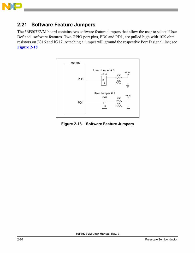
2.21 Software Feature Jumpers
The 56F807EVM board contains two software feature jumpers that allow the user to select “User
Defined” software features. Two GPIO port pins, PD0 and PD1, are pulled high with 10K ohm
resistors on JG16 and JG17. Attaching a jumper will ground the respective Port D signal line; see
Figure 2-18.
56F807
PD0
PD1
JG16
JG17
12
3
12
3
10K
10K
10K
10K
+3.3V
+3.3V
User Jumper # 0
User Jumper # 1
Figure 2-18. Software Feature Jumpers
Peripheral Connectors
Technical Summary, Rev. 3
Freescale Semiconductor 2-27
2.22 Peripheral Connectors
The EVM board contains a group of Peripheral Expansion Connectors used to gain access to the
resources of the 56F807. These signal groups have Expansion Connectors:
• Port B
• Port D
• Port E
• External Memory Control
• Encoder A/Timer Channel A
• Encoder B/Timer Channel B
• Timer Channel C
• Timer Channel D
• Port A/Address Bus
• Data Bus
• A/D Input Port A
• A/D Input Port B
• Serial Communications Port 0
• Serial Communications Port 1
• Serial Peripheral Port
• PWM Port A
• PWM Port B
56F807EVM User Manual, Rev. 3
2-28 Freescale Semiconductor
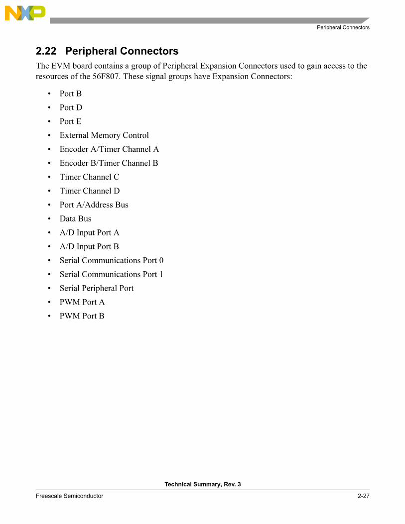
2.22.1 Port B Expansion Connector
Port B is a GPIO port which is connected to the Port B header. The pins of the port, PB0-PB7, are
dedicated to general purpose I/O and Interrupt operations. The GPIO port pins may be
programmed as inputs, outputs or level-sensitive interrupt inputs. Table 2-12 shows the port pin
to headed connections.
Table 2-12. Port B Connector Description
J20
Pin # Signal Pin # Signal
1 PB0 2 PB1
3 PB2 4 PB3
5 PB4 6 PB5
7 PB6 8 PB7
9 GND 10 +3.3V
2.22.2 Port D Expansion Connector
Port D is an MPIO port with signal lines attached to various headers. The six pins of the port,
PD0-PD5, are dedicated to general purpose operation. The remaining two pins, PD6 and PD7, are
shared with the TXD1 and RXD1 signal lines. The GPIO port pins may be programmed as
inputs, outputs or level-sensitive interrupt inputs. Table 2-13 shows the exclusive Port D signals.
The shared Port D signals are contained in Table 2-20.
Table 2-13. Port D Connector Description
J23
Pin # Signal Pin # Signal
1 PD0 2 PD1
3 PD2 4 PD3
5 PD4 6 PD5
7 GND 8 +3.3V
Peripheral Connectors
Technical Summary, Rev. 3
Freescale Semiconductor 2-29
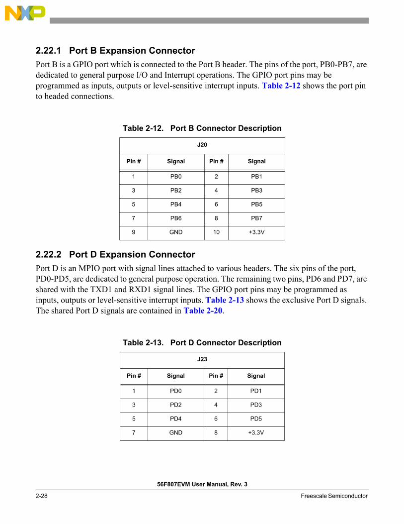
2.22.3 Port E Expansion Connector
Port E is an MPIO port with signal lines attached to various headers. The pins of the port are
shared with one SCI port, SCI0, two Address bus lines, A6 and A7, and the SPI port. Table 2-14
shows the shared pins and functions.
Table 2-14. Port E Connector Description
J17
Pin # Signal Alternate Funct Pin # Signal Alternate Funct
1 PE0 TXD0 2 PE1 RXD0
3 PE2 TXD1 4 PE3 RXD1
5 PE4 SCLK 6 PE5 MOSI
7 PE6 MISO 8 PE7 SS
9 GND GND 10 +3.3V +3.3V
2.22.4 External Memory Control Signal Expansion Connector
The External Memory Control Signal connector contains the device’s external memory control
signal lines. Refer to Table 2-15 for the names of these signals.
Table 2-15. External Memory Control Signal Connector Description
J8
Pin # Signal Pin # Signal
1 RD 2 IRQA
3 WR 4 IRQB
5 PS 6 RESET
7 DS 8 RSTO
9 CLKO 10 DE
11 GND 12 +3.3V
56F807EVM User Manual, Rev. 3
2-30 Freescale Semiconductor
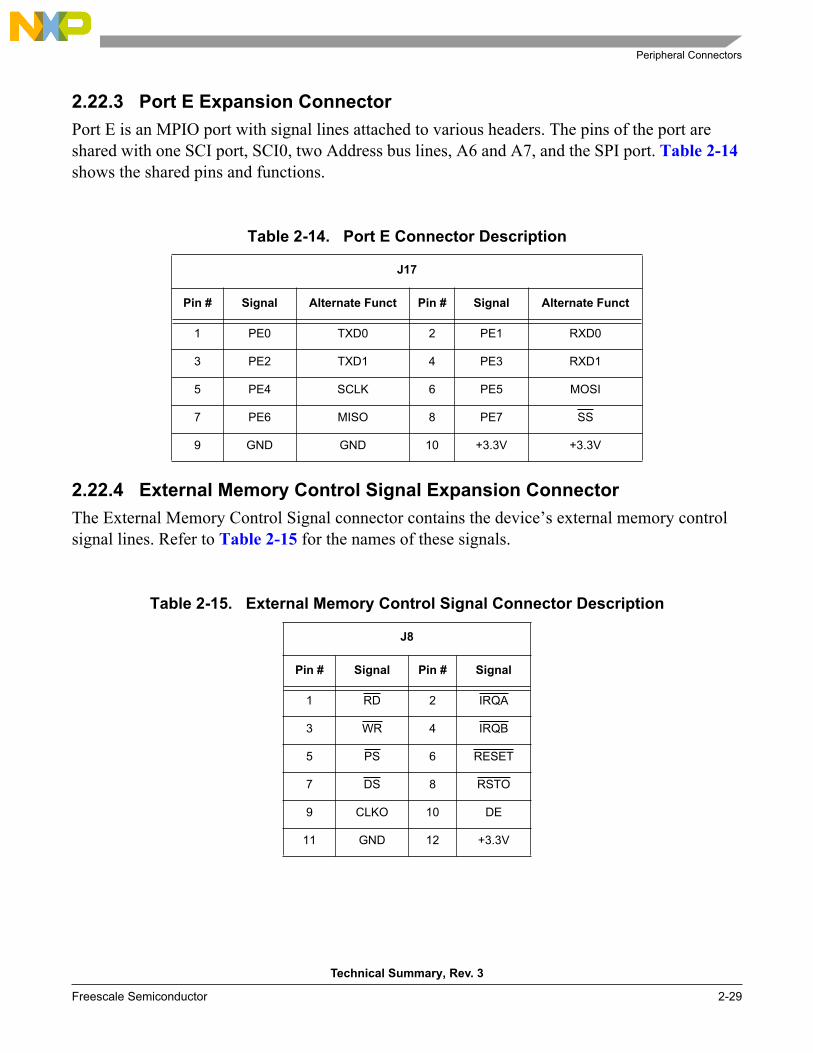
2.22.5 Primary Encoder/Timer Channel A Expansion Connector
The Primary Encoder/Timer Channel A port is an MPIO port attached to the Timer A expansion
connector. The port can act as a Quadrature Decoder interface port or as a general purpose Timer
port. See Table 2-16 for the signals attached to the connector.
Table 2-16. Timer A Connector Description
J18
Pin # Signal Alternate
1 TA0 PhaseA0
2 TA1 PhaseB0
3 TA2 INDEX0
4 TA3 HOME0
5 +3.3V +3.3V
6 GND GND
2.22.6 Secondary Encoder/Timer Channel B Expansion Connector
The Secondary Encoder/Timer Channel B port is an MPIO port attached to the Timer B
expansion connector. The port can act as a Quadrature Decoder interface port or as a general
purpose Timer port. Refer to Table 2-17 for the signals attached to the connector.
Table 2-17. Timer B Connector Description
J21
Pin # Signal Alternate
1 TB0 PhaseA1
2 TB1 PhaseB1
3 TB2 INDEX1
4 TB3 HOME1
5 +3.3V +3.3V
6 GND GND
Peripheral Connectors
Technical Summary, Rev. 3
Freescale Semiconductor 2-31
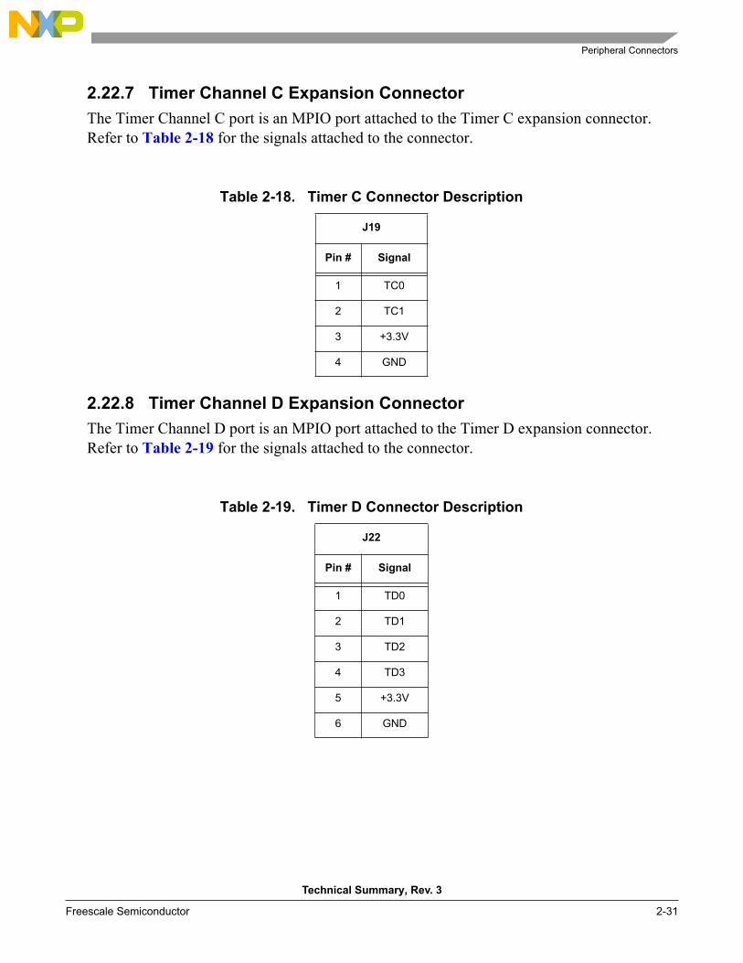
2.22.7 Timer Channel C Expansion Connector
The Timer Channel C port is an MPIO port attached to the Timer C expansion connector.
Refer to Table 2-18 for the signals attached to the connector.
Table 2-18. Timer C Connector Description
J19
Pin # Signal
1 TC0
2 TC1
3 +3.3V
4 GND
2.22.8 Timer Channel D Expansion Connector
The Timer Channel D port is an MPIO port attached to the Timer D expansion connector.
Refer to Table 2-19 for the signals attached to the connector.
Table 2-19. Timer D Connector Description
J22
Pin # Signal
1 TD0
2 TD1
3 TD2
4 TD3
5 +3.3V
6 GND
56F807EVM User Manual, Rev. 3
2-32 Freescale Semiconductor
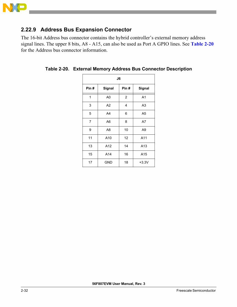
2.22.9 Address Bus Expansion Connector
The 16-bit Address bus connector contains the hybrid controller’s external memory address
signal lines. The upper 8 bits, A8 - A15, can also be used as Port A GPIO lines. See Table 2-20
for the Address bus connector information.
Table 2-20. External Memory Address Bus Connector Description
J6
Pin # Signal Pin # Signal
1 A0 2 A1
3 A2 4 A3
5 A4 6 A5
7 A6 8 A7
9 A8 10 A9
11 A10 12 A11
13 A12 14 A13
15 A14 16 A15
17 GND 18 +3.3V
Peripheral Connectors
Technical Summary, Rev. 3
Freescale Semiconductor 2-33
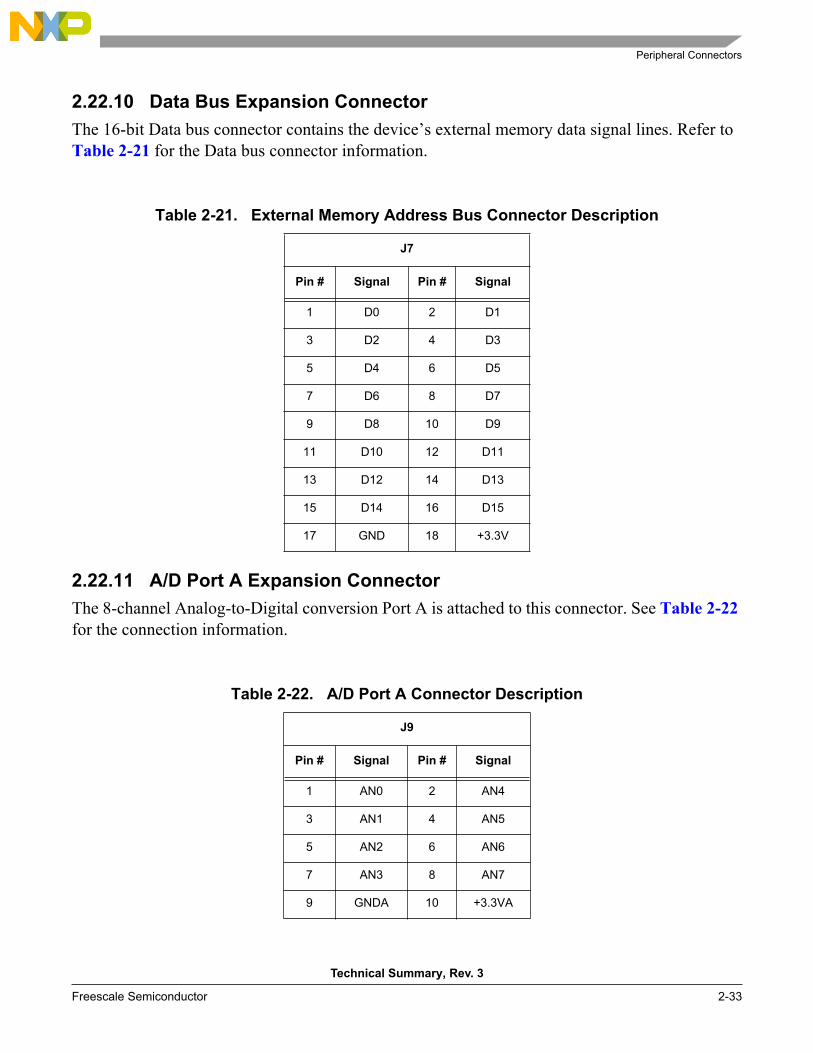
2.22.10 Data Bus Expansion Connector
The 16-bit Data bus connector contains the device’s external memory data signal lines. Refer to
Table 2-21 for the Data bus connector information.
Table 2-21. External Memory Address Bus Connector Description
J7
Pin # Signal Pin # Signal
1 D0 2 D1
3 D2 4 D3
5 D4 6 D5
7 D6 8 D7
9 D8 10 D9
11 D10 12 D11
13 D12 14 D13
15 D14 16 D15
17 GND 18 +3.3V
2.22.11 A/D Port A Expansion Connector
The 8-channel Analog-to-Digital conversion Port A is attached to this connector. See Table 2-22
for the connection information.
Table 2-22. A/D Port A Connector Description
J9
Pin # Signal Pin # Signal
1 AN0 2 AN4
3 AN1 4 AN5
5 AN2 6 AN6
7 AN3 8 AN7
9 GNDA 10 +3.3VA
56F807EVM User Manual, Rev. 3
2-34 Freescale Semiconductor
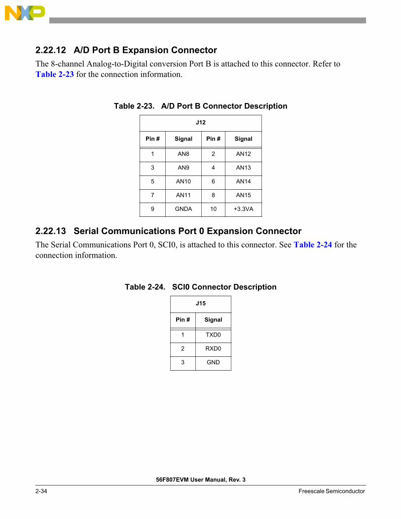
2.22.12 A/D Port B Expansion Connector
The 8-channel Analog-to-Digital conversion Port B is attached to this connector. Refer to
Table 2-23 for the connection information.
Table 2-23. A/D Port B Connector Description
J12
Pin # Signal Pin # Signal
1 AN8 2 AN12
3 AN9 4 AN13
5 AN10 6 AN14
7 AN11 8 AN15
9 GNDA 10 +3.3VA
2.22.13 Serial Communications Port 0 Expansion Connector
The Serial Communications Port 0, SCI0, is attached to this connector. See Table 2-24 for the
connection information.
Table 2-24. SCI0 Connector Description
J15
Pin # Signal
1 TXD0
2 RXD0
3 GND
Peripheral Connectors
Technical Summary, Rev. 3
Freescale Semiconductor 2-35
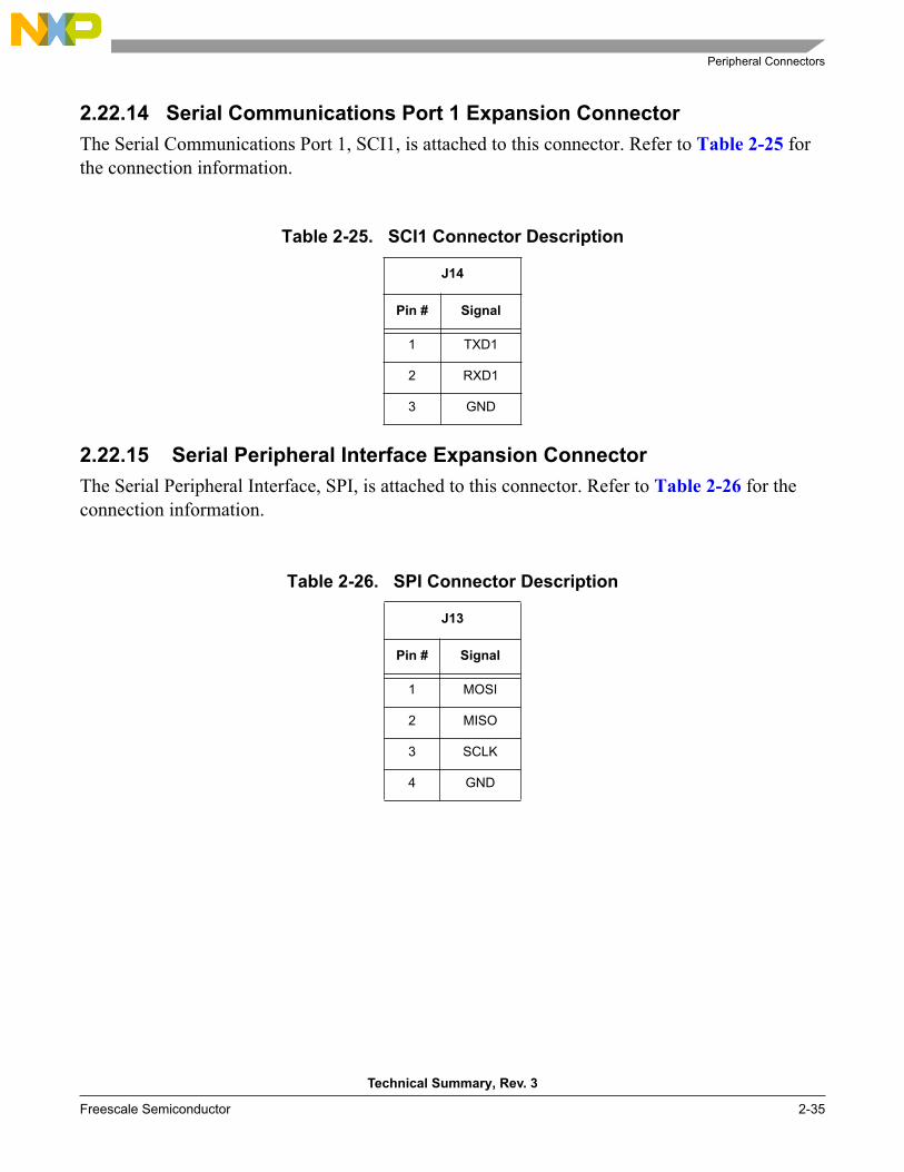
2.22.14 Serial Communications Port 1 Expansion Connector
The Serial Communications Port 1, SCI1, is attached to this connector. Refer to Table 2-25 for
the connection information.
Table 2-25. SCI1 Connector Description
J14
Pin # Signal
1 TXD1
2 RXD1
3 GND
2.22.15 Serial Peripheral Interface Expansion Connector
The Serial Peripheral Interface, SPI, is attached to this connector. Refer to Table 2-26 for the
connection information.
Table 2-26. SPI Connector Description
J13
Pin # Signal
1 MOSI
2 MISO
3 SCLK
4 GND
56F807EVM User Manual, Rev. 3
2-36 Freescale Semiconductor
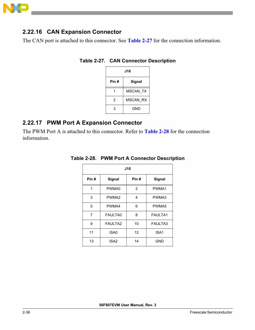
2.22.16 CAN Expansion Connector
The CAN port is attached to this connector. See Table 2-27 for the connection information.
Table 2-27. CAN Connector Description
J16
Pin # Signal
1 MSCAN_TX
2 MSCAN_RX
3 GND
2.22.17 PWM Port A Expansion Connector
The PWM Port A is attached to this connector. Refer to Table 2-28 for the connection
information.
Table 2-28. PWM Port A Connector Description
J10
Pin # Signal Pin # Signal
1 PWMA0 2 PWMA1
3 PWMA2 4 PWMA3
5 PWMA4 6 PWMA5
7 FAULTA0 8 FAULTA1
9 FAULTA2 10 FAULTA3
11 ISA0 12 ISA1
13 ISA2 14 GND
Test Points
Technical Summary, Rev. 3
Freescale Semiconductor 2-37
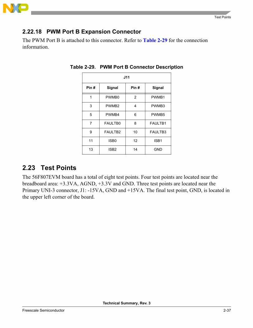
2.22.18 PWM Port B Expansion Connector
The PWM Port B is attached to this connector. Refer to Table 2-29 for the connection
information.
Table 2-29. PWM Port B Connector Description
J11
Pin # Signal Pin # Signal
1 PWMB0 2 PWMB1
3 PWMB2 4 PWMB3
5 PWMB4 6 PWMB5
7 FAULTB0 8 FAULTB1
9 FAULTB2 10 FAULTB3
11 ISB0 12 ISB1
13 ISB2 14 GND
2.23 Test Points
The 56F807EVM board has a total of eight test points. Four test points are located near the
breadboard area: +3.3VA, AGND, +3.3V and GND. Three test points are located near the
Primary UNI-3 connector, J1: -15VA, GND and +15VA. The final test point, GND, is located in
the upper left corner of the board.

56F807EVM User Manual, Rev. 3
2-38 Freescale Semiconductor
Appendix A, Rev. 3
Freescale Semiconductor A-1
Appendix A56F807EVM Schematics
A A
B B
C C
D D
E E
44
33
22
11
JTAG
CAN
Primary PFC_ENABLE
Secondary PFC_ENABLE
Secondary ZERO_CROSSING
Primary PFC_PWM
Primary PFC_ZERO_CROSSING
Secondary PFC_PWM
Primary serial_com
SECONDARY serial_con
USER LED: RED
USER LED: YELLOW
USER LED: GREEN
SERIAL D/A /CS
SECONDARY UNI-3 BRAKE CONTROL
GP PUSH BUTTON 2
START/STOP SW
USER JUMPER #1
USER JUMPER #2
GP PUSH BUTTON 1
Primary UNI-3 PWM 1
Primary UNI-3 PWM 2
Primary UNI-3 PWM 3
Primary UNI-3 PWM 4
Primary UNI-3 PWM 5
Primary UNI-3 OVER VOLTAGE
Primary UNI-3 PHASE A OVER CURRENT
Primary UNI-3 PHASE B OVER CURRENT
Primary UNI-3 PHASE C OVER CURRENT
Primary UNI-3 PWM 0
PRIMARY ENCODER
HALL EFFECT /
ZERO CROSSING
Secondary UNI-3 PWM 1
Secondary UNI-3 OVER VOLTAGE
Secondary UNI-3 PHASE A OVER CURRENT
Secondary UNI-3 PWM 2
Secondary UNI-3 PWM 3
Secondary UNI-3 PWM 4
Secondary UNI-3 PWM 5
Secondary UNI-3 PWM 0
Secondary UNI-3 PHASE B OVER CURRENT
Secondary UNI-3 PHASE C OVER CURRENT
Primary U3_I/BK_EMF_SENSE_C
Primary U3_V_SENSE_DCB
Primary U3_I/BK_EMF_SENSE_B
Primary U3_TEMP_SENSE
Primary U3_I_SENSE_DCB
SECONDARY ENCODER
HALL EFFECT /
ZERO CROSSING
Secondary U3_I_SENSE_DCB
Secondary U3_I/BK_EMF_SENSE_C
Secondary U3_I/BK_EMF_SENSE_A
Secondary U3_TEMP_SENSE
Secondary U3_V_SENSE_DCB
Secondary U3_I/BK_EMF_SENSE_B
PRIMARY UNI-3 BRAKE CONTROL
Primary U3_I/BK_EMF_SENSE_A
DS
PD
Des
ign
DS
P56
F807
Pro
cess
or
63A
1051
6S
1.0
118
Mon
day,
Oct
ober
16,
200
0B
DS
P S
tand
ard
Pro
duct
s D
ivis
ion
2100
Eas
t Elli
ot R
oad
Tem
pe, A
rizon
a 85
284
Title
Doc
umen
t
Dat
e:
Siz
e
Des
igne
r:S
heet
of
Rev
.N
umbe
r
(480
) 41
3-50
90
FAX
: (48
0) 4
13-2
510
A0
A1
A2
A3
A4
A5
A6
A7
A8
A9
A10
A11
A12
A13
A14
A15
D0
D1
D2
D3
D4
D5
D6
D7
D8
D9
D10
D11
D12
D13
D14
D15
TC
ST
CS
TC
S
A[0
..15
]
D[0
..15
]
MS
CA
N_R
XM
SC
AN
_TX
DE
BU
G_E
VE
NT
SC
LKM
OS
IM
ISO
/SS
/TR
ST
TD
OT
DI
TMS
TC
K
/PS
/DS
/WR
/RD
/IR
QA
/IR
QB
EX
TBO
OT
CLK
OE
XTA
LX
TAL
/RE
SE
T/R
ST
O
TC
0T
C1
TD
1T
D0
TD
3T
D2
TXD
1R
XD
1
RX
D0
TXD
0
PB
0P
B1
PB
2P
B3
PB
4
PB
6P
B7
PB
5
PD
2P
D3
PD
4P
D5
PD
0P
D1
PW
MA
1P
WM
A2
PW
MA
5
ISA
1IS
A0
ISA
2F
AU
LTA
0
FA
ULT
A3
FA
ULT
A1
FA
ULT
A2
PW
MA
0
PW
MA
4P
WM
A3
PH
AS
EA
0
HO
ME
0IN
DE
X0
PH
AS
EB
0
PW
MB
1P
WM
B2
PW
MB
3
PW
MB
5
ISB
1IS
B2
FA
ULT
B0
FA
ULT
B3
FA
ULT
B1
FA
ULT
B2
PW
MB
4
PW
MB
0
ISB
0
AN
6
AN
0
AN
7
AN
2A
N1
AN
5A
N4
AN
3
HO
ME
1IN
DE
X1
PH
AS
EA
1P
HA
SE
B1
AN
13
AN
15
AN
11
AN
9A
N10
AN
8
AN
12
AN
14
+3.
3VA
+3.
3VA
+3.3
V
+3.
3VA
+3.3
VA
+C
12.
2uF
+C
22.
2uF
C7
0.1u
F
C8
0.1u
F
U1A
DS
P56
F80
7FV
80
1 2 3 4 5 6 7 8 10 11 12 13 14 15 16 17 19 20 21 2223 24 25 26 27 28 29 30 31 32 33 35 36 37 38 39
40 41 42 43 44 45 46 47 49 50 51 52 53 54
55 56
57 58 59 60 61 62 64 66 67
69 70
71 72 73 7475 77 78 79 80 81 82 83 84 85
86 92 93 9798
123
124
125
102
103
104
105
106
107
108
109
99 113
114
115
116
117
118
119
120
110
121
126
127
128
129
130
131
132
133
134
135
136
137
143
144
145
146
139
142
147
148
149
150
151
152
154
155
159
160
158
A0
A1
A2
A3
A4
A5
A6
A7
A8
A9
A10
A11
A12
A13
A14
A15
PS
DS
WR
RD
D0
D1
D2
D3
D4
D5
D6
D7
D8
D9
D10
D11
D12
D13
D14
D15
MP
IOB
0M
PIO
B1
MP
IOB
2M
PIO
B3
MP
IOB
4M
PIO
B5
MP
IOB
6M
PIO
B7
MP
IOD
0M
PIO
D1
MP
IOD
2M
PIO
D3
MP
IOD
4M
PIO
D5
TX
D1
RX
D1
PW
MB
0P
WM
B1
PW
MB
2P
WM
B3
PW
MB
4P
WM
B5
ISB
0IS
B1
ISB
2
IRQ
AIR
QB
FA
ULT
B0
FA
ULT
B1
FA
ULT
B2
FA
ULT
B3
PW
MA
0P
WM
A1
PW
MA
2P
WM
A3
PW
MA
4P
WM
A5
FA
ULT
A0
FA
ULT
A1
FA
ULT
A2
FA
ULT
A3
XB
OO
T
XT
AL
EX
TA
L
RS
TO
RE
SE
T
ISA
0IS
A1
ISA
2
AN
A0
AN
A1
AN
A2
AN
A3
AN
A4
AN
A5
AN
A6
AN
A7
VR
H
AN
A8
AN
A9
AN
A10
AN
A11
AN
A12
AN
A13
AN
A14
AN
A15
VR
H2
DE
TD
0T
D1
TD
2T
D3
TC
0T
C1
TR
ST
TC
S
TC
K
TM
S
TD
IT
DO
SS
SC
LK
MIS
OM
OS
IM
SC
AN
_TX
MS
CA
N_
RX
PH
A0
PH
B0
IND
EX
0H
OM
E0
PH
A1
PH
B1
IND
EX
1H
OM
E1
TX
D0
RX
D0
CL
KO
U1B
DS
P56
F80
7FV
80
9 34 63 94 153
140
89
18 48 76 95 157
141 91 90 122
65 138
88 8796
100
101
111
112
156 68
VD
D_I
O1
VD
D_I
O2
VD
D_I
O3
VD
D_I
O4
VD
D_I
O5
VD
D_I
O6
VD
D_I
O7
VS
S_I
O1
VS
S_I
O2
VS
S_I
O3
VS
S_I
O4
VS
S_I
O5
VS
S_I
O6
VS
S_I
O7
VS
S_I
O8
VS
S_I
O9
VC
AP
C1
VC
AP
C2
VD
DA
_A
RE
G1
VS
SA
_AR
EG
1
VD
DA
_C
OR
E1
VD
DA
_AD
C2
VS
SA
_AD
C2
VD
DA
_AD
C1
VS
SA
_AD
C1
VP
PV
PP
2
R12
4
1K
56F807EVM User Manual, Rev. 3
A-2 Freescale Semiconductor
Fig
ure
A-1
.
56F
807 P
rocesso
r
A A
B B
C C
D D
E E
44
33
22
11
IRQA PUSHBUTTON
OSC BYPASS
IRQB PUSHBUTTON
RESET PUSHBUTTON
BO
OT
MO
DE
JU
MP
ER
INT BOOT
EXT BOOT
NC
1 - 2
12
3
DS1818
OPTIONAL
DS
PD
Des
ign
RE
SE
T,
MO
DE
, C
LO
CK
& I
RQ
S
63
A1
05
16
S
1.0
218
Mon
day,
Oct
ober
16,
200
0A
DS
P S
tan
dar
d P
rod
uct
s D
ivis
ion
2100
Eas
t E
lliot
Roa
dT
empe
, A
rizo
na 8
5284
Titl
e
Do
cum
en
t
Da
te:
Siz
e
De
sig
ner
:S
he
et
of
Re
v.N
um
be
r
(480
) 41
3-50
90
F
AX
: (4
80)
413-
2510
/PO
R
/PO
R
/IR
QA
/IR
QB
EX
TB
OO
T
EX
TA
L
XT
AL
+3
.3V
+3
.3V
+3
.3V
+3
.3V
+3
.3V
JG5
12
3
Y1
8.0
0M
Hz
S1
S2
S3
R8
41
0K
R8
31
0K
R8
21
0K
R1
10
M
JG7 12
JG6
12
U1
7
DS
18
18
DN
P
21
3
Vcc
RS
TG
ND
C6
70
.1u
F
C6
80
.1u
F
R1
25
10
K
Appendix A, Rev. 3
Freescale Semiconductor A-3
Fig
ure
A-2
. R
eset,
Mo
de,C
lock &
IR
QS
A A
B B
C C
D D
E E
44
33
22
11
64Kx16-bit Program and 64Kx16-bit Data Memory
SR
AM
EN
AB
LE
JU
MP
ER
OPTION
JG8
SRAM ENABLE
SRAM DISABLE
1 - 2
NC
DS
PD
Des
ign
PR
OG
RA
M &
DA
TA
SR
AM
ME
MO
RY
63
A1
05
16
S1.
03
18M
onda
y, O
ctob
er 1
6, 2
000
A
DS
P S
tan
dar
d P
rod
uct
s D
ivis
ion
2100
Eas
t E
lliot
Roa
dT
empe
, A
rizo
na 8
5284
Titl
e
Do
cum
en
t
Da
te:
Siz
e
De
sig
ner
:S
he
et
of
Re
v.N
um
be
r
(480
) 41
3-50
90
F
AX
: (4
80)
413-
2510
D2
D5
D1
3
D4
D0
D6
D1
5
D1
1
D3
D1
0
D1
D7
D1
2
D9
D8
D1
4
A1
5
A1
1
A1
A1
2
A1
0
A3
A1
4
A5
A9
A6
A8
A0
A7
A1
3
A2
A4
/RD
/WR
D[0
..1
5]
A[0
..1
5]
/PS
+3
.3V
+3
.3V
U2
GS
72
11
6T
P-1
2
7 8
1
9 10
21
31
4
3
15
16
4
29
30
5
31
32
18
35
36
19
37
38
20
21
24
25
26
27
42
43
44
40
39
41
17 6
22
34
12
33
11
DQ
1D
Q2
A4
DQ
3D
Q4
A3
DQ
5D
Q6
A2
DQ
7D
Q8
A1
DQ
9D
Q1
0
A0
DQ
11
DQ
12
A1
5
DQ
13
DQ
14
A1
4D
Q1
5D
Q1
6
A1
3A
12
A1
1A
10
A9
A8
A7
A6
A5
UB
LB
OE
WE
CE
A1
6
VS
SV
SS
VD
DV
DD
JG8 1 2
R8
51
0K
R8
71
KR
86
1K
56F807EVM User Manual, Rev. 3
A-4 Freescale Semiconductor
Fig
ure
A-3
.
Pro
gra
m &
Data
SR
AM
Mem
ory
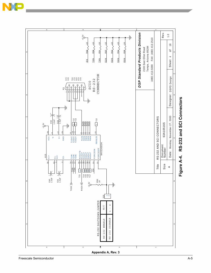
A A
B B
C C
D D
E E
44
33
22
11
RS
-23
2 S
HU
TD
OW
N J
UM
PE
R
1 - 2
N/C
RS-232 ENABLE
RS-232 DISABLE
CONNECTOR
CTS
DSR
DTR
RXD
TXD
RTS
DCD
+
+
+ +
SCI0
RS-232
DS
PD
Des
ign
RS
-23
2 A
ND
SC
I C
ON
NE
CT
OR
S
63
A1
05
16
S
1.0
418
Mon
day,
Nov
embe
r 27
, 20
00A
DS
P S
tan
dar
d P
rod
uct
s D
ivis
ion
2100
Eas
t E
lliot
Roa
dT
empe
, A
rizo
na 8
5284
Titl
e
Do
cum
en
t
Da
te:
Siz
e
De
sig
ner
:S
he
et
of
Re
v.N
um
be
r
(480
) 41
3-50
90
F
AX
: (4
80)
413-
2510
R4
IN
R5
IN
R2
IN
R3
IN
T3
IN
/EN
T2
IN
T2
INT
3IN
/EN
R3
INR
4IN
R5
IN
R2
IN
TX
D0
RX
D0
+3
.3V
+3
.3V
+3
.3V
R9
41
K
R9
51
K
R9
31
K
R9
21
K
R8
91
K
R9
11
K
R8
81
K
C6
01
.0u
F
C6
11
.0u
FC
63
1.0
uF
C6
2
1.0
uF
JG9 1 2
R9
01
K
T1
41
T1
51
T1
61
T1
71
P3
594837261
T1
31
T1
21
T2
21
T2
11
U1
3 MA
X3
24
5E
EA
I
27
1
26
2
23
28
14
13
12
19
18
17
16
15
8765411
10
9
22
24
3 25
20
21
V+
C2
+
VC
C
C2
-
FO
RC
EO
N
C1
+
T1
INT
2IN
T3
IN
R1
OU
TR
2O
UT
R3
OU
TR
4O
UT
R5
OU
TR
5IN
R4
INR
3IN
R2
INR
1IN
T3
OU
TT
2O
UT
T1
OU
T
FO
RC
EO
FF
C1
-V
-
GN
D
R2
OU
TB
INV
AL
ID
Appendix A, Rev. 3
Freescale Semiconductor A-5
Fig
ure
A-4
. R
S-2
32 a
nd
SC
I C
on
necto
rs
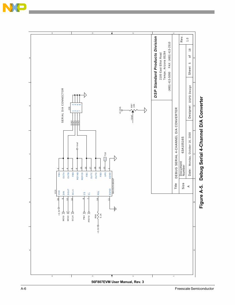
A A
B B
C C
D D
E E
44
33
22
11
SE
RIA
L D
/A C
ON
NE
CT
OR
DS
PD
Des
ign
DE
BU
G S
ER
IAL
4-C
HA
NN
EL
D/A
CO
NV
ER
TE
R
63
A1
05
16
S
1.0
518
Mon
day,
Oct
ober
16,
200
0A
DS
P S
tan
dar
d P
rod
uct
s D
ivis
ion
2100
Eas
t E
lliot
Roa
dT
empe
, A
rizo
na 8
5284
Titl
e
Do
cum
en
t
Da
te:
Siz
e
De
sig
ner
:S
he
et
of
Re
v.N
um
be
r
(480
) 41
3-50
90
F
AX
: (4
80)
413-
2510
D/A
3D
/A2
D/A
1D
/A0
+V
ref
MIS
O
SC
LK
MO
SI
PB
4
/RS
TO
+3
.3V
+3
.3V
+3
.3V
A
+V
ref
R9
6
5.1
K
U1
4
MA
X5
25
1B
EA
P
12 3 4 5 6 15
16
17
18
19
20
13
9
12
10 8 7
14
11
AG
ND
FB
A
OU
TA
OU
TB
FB
B
RE
FA
B
RE
FC
D
FB
C
OU
TC
OU
TD
FB
D
VD
D
UP
0
DIN
DO
UT
SC
LK
CS
CL
PD
L
DG
ND
J26
1 3 5 7
2 4 6 8
T1
81
R9
71
0K
56F807EVM User Manual, Rev. 3
A-6 Freescale Semiconductor
Fig
ure
A-5
. D
eb
ug
Seri
al 4-C
han
nel D
/A C
on
vert
er
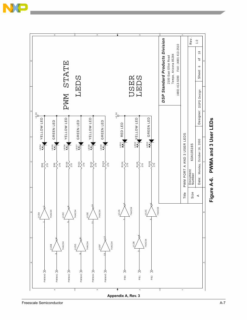
A A
B B
C C
D D
E E
44
33
22
11
PWM STATE
LEDS
USER
LEDS
YE
LL
OW
LE
D
YE
LL
OW
LE
D
RE
D L
ED
GR
EE
N L
ED
GR
EE
N L
ED
GR
EE
N L
ED
GR
EE
N L
ED
YE
LL
OW
LE
D
YE
LL
OW
LE
D
DS
PD
Des
ign
PW
M P
OR
T A
AN
D 3
US
ER
LE
DS
63
A1
05
16
S
1.0
618
Mon
day,
Oct
ober
16,
200
0A
DS
P S
tan
dar
d P
rod
uct
s D
ivis
ion
2100
Eas
t E
lliot
Roa
dT
empe
, A
rizo
na 8
5284
Titl
e
Do
cum
en
t
Da
te:
Siz
e
De
sig
ner
:S
he
et
of
Re
v.N
um
be
r
(480
) 41
3-50
90
F
AX
: (4
80)
413-
2510
PW
MA
4
PW
MA
1
PW
MA
0
PW
MA
5
PW
MA
2
PW
MA
3
PB
0
PB
1
PB
2
+3
.3V
+3
.3V
R9
8
27
0
R9
9
27
0
R1
00
27
0
R1
01
27
0
R1
02
27
0
R1
03
27
0
R1
04
27
0
R1
05
27
0
R1
06
27
0
U1
5A
74
AC
04
12
U1
5B
74
AC
04
34
U1
5C
74
AC
04
56
U1
5D
74
AC
04
98
U1
5E
74
AC
04
11
10
U1
5F
74
AC
04
13
12
U1
2A
74
AC
04
12
U1
2B
74
AC
04
34
U1
2C
74
AC
04
56
LE
D4
LE
D5
LE
D6
LE
D7
LE
D8
LE
D9
LE
D1
LE
D2
LE
D3
Appendix A, Rev. 3
Freescale Semiconductor A-7
Fig
ure
A-6
.
PW
MA
an
d 3
Us
er
LE
Ds
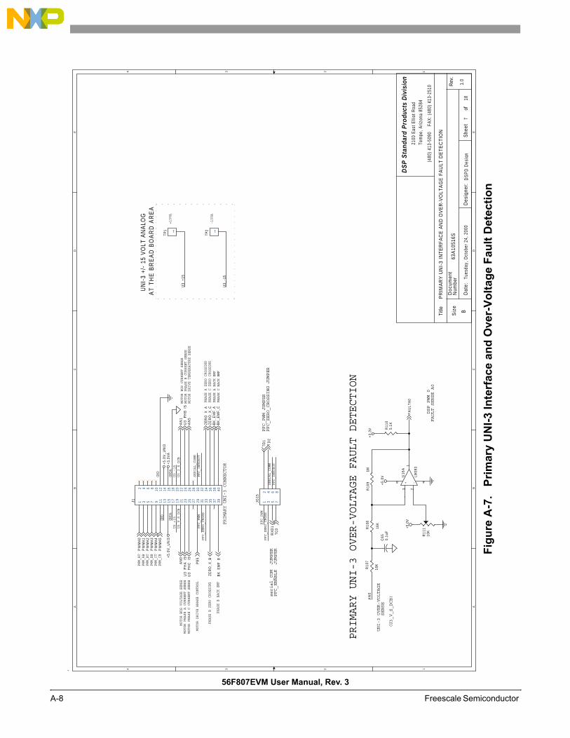
A A
B B
C C
D D
E E
44
33
22
11
PRIMARY UNI-3 CONNECTOR
PFC_ZERO_CROSSING JUMPER
PFC_PWM JUMPER
PFC_ENABLE JUMPER
serial_COM JUMPER
PHASE B BACK EMF
PHASE C BACK EMF
MOTOR PHASE A CURRENT SENSE
MOTOR DRIVE TEMPERATURE SENSE
MOTOR PHASE C CURRENT SENSE
MOTOR DRIVE BRAKE CONTROL
PWM_AT
PWM_AB
PWM_BT
PWM_BB
PWM_CT
PWM_CB
MOTOR PHASE B CURRENT SENSE
PRIMARY UNI-3 OVER-VOLTAGE FAULT DETECTION
UNI-3 OVER-VOLTAGE
SENSE
FAULT SENSE A0
DSP PWM 0
MOTOR BUS VOLTAGE SENSE
MOTOR BUS CURRENT SENSE
UN
I-3
+/-
15 V
OLT
AN
ALO
GA
T T
HE
BR
EA
D B
OA
RD
AR
EA
+15VA
-15VA
U3_V_S_DCB
U3_I_S_DCB
(U3_V_S_DCB)
PHASE A BACK EMF
PHASE C ZERO CROSSING
PHASE A ZERO CROSSING
PHASE B ZERO CROSSING
DS
PD
Des
ign
PR
IMA
RY
UN
I-3
INTE
RFA
CE
AN
D O
VE
R-V
OLT
AG
E F
AU
LT D
ETE
CTI
ON
63A
1051
6S
1.0
718
Tues
day,
Oct
ober
24,
200
0B
DS
P S
tand
ard
Pro
duct
s D
ivis
ion
2100
Eas
t Elli
ot R
oad
Tem
pe, A
rizon
a 85
284
Title
Doc
umen
t
Dat
e:
Siz
e
Des
igne
r:S
heet
of
Rev
.N
umbe
r
(480
) 41
3-50
90
FAX
: (48
0) 4
13-2
510
GND
GND
GNDA
GNDA
PFC_PWM
PFC_ZERO_CROSS
SERIAL_COMM
PFC_INHIBIT
PFC_ZERO_CROSS
PFC_PWM
SERIAL_COMM
PFC_INHIBIT
AN
0
U3_-15
U3_+15
U3_
+15
U3_
-15
PW
MA
0P
WM
A1
PW
MA
2P
WM
A3
PW
MA
4
U3_
PH
B_I
SU
3_P
HC
_IS
AN
5
ZE
RO
_X_A
ZE
RO
_X_B
ZE
RO
_X_C
BK
_EM
F_A
BK
_EM
F_B
BK
_EM
F_C
PB
5
RX
D1
TD
1
TC
0
U3_
PH
A_I
S
TD
2
PW
MA
5
FA
ULT
A0
AN
0A
N1
+5.
0V_U
NI3
+5.
0V_U
NI3
+3.3
VA
+3.
3V
+5.
0V
+5.0
V
JG15
1 3 5 7
2 4 6 8
J1 1 3 5 7 9 11 13 15 17 19 21 23 25 27 29 31 33 35 37 39
2 4 6 8 10 12 14 16 18 20 22 24 26 28 30 32 34 36 38 40
C65
0.1u
FR
110
5.1K
R10
7
16K
R10
8
16K
R10
91M
+ -
U16
A
LM39
3
3 21
8 4
TP1 1
TP2 1
R11
110
K
56F807EVM User Manual, Rev. 3
A-8 Freescale Semiconductor
d
Fig
ure
A-7
. P
rim
ary
UN
I-3 In
terf
ace a
nd
Over-
Vo
ltag
e F
au
lt D
ete
cti
on
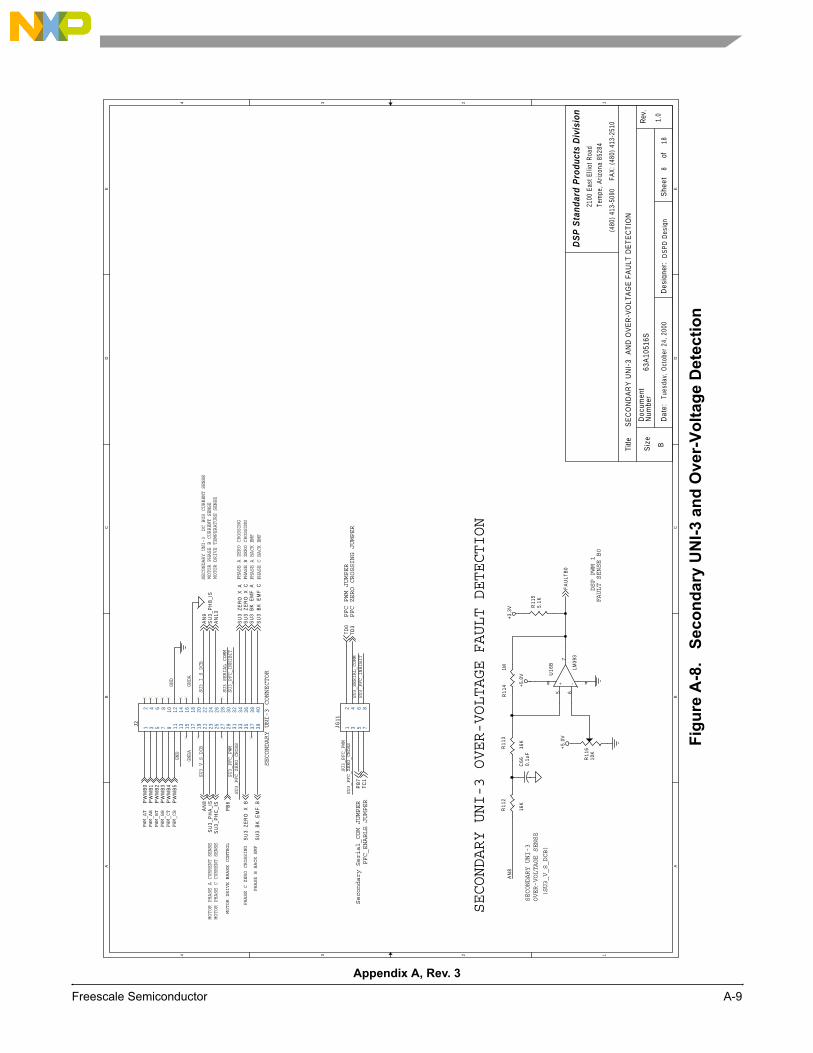
A A
B B
C C
D D
E E
44
33
22
11
SECONDARY UNI-3 CONNECTOR
PFC ZERO CROSSING JUMPER
PFC PWM JUMPER
PFC_ENABLE JUMPER
Secondary Serial_COM JUMPER
PHASE B BACK EMF
PHASE C BACK EMF
PHASE A BACK EMF
MOTOR PHASE A CURRENT SENSE
MOTOR DRIVE TEMPERATURE SENSE
MOTOR PHASE C CURRENT SENSE
MOTOR DRIVE BRAKE CONTROL
PWM_AT
PWM_AB
PWM_BT
PWM_BB
PWM_CT
PWM_CB
MOTOR PHASE B CURRENT SENSE
PHASE A ZERO CROSSING
PHASE B ZERO CROSSING
PHASE C ZERO CROSSING
SECONDARY UNI-3 OVER-VOLTAGEFAULT DETECTION
FAULT SENSE B0
DSP PWM 1
SECONDARY UNI-3 DC BUS CURRENT SENSE
SU3_V_S_DCB
SU3_I_S_DCB
SECONDARY UNI-3
OVER-VOLTAGE SENSE
(SU3_V_S_DCB)
DS
PD
Des
ign
SE
CO
ND
AR
Y U
NI-
3 A
ND
OV
ER
-VO
LTA
GE
FA
ULT
DE
TEC
TIO
N
63A
1051
6S
1.0
818
Tues
day,
Oct
ober
24,
200
0B
DS
P S
tand
ard
Pro
duct
s D
ivis
ion
2100
Eas
t Elli
ot R
oad
Tem
pe, A
rizon
a 85
284
Title
Doc
umen
t
Dat
e:
Siz
e
Des
igne
r:S
heet
of
Rev
.N
umbe
r
(480
) 41
3-50
90
FAX
: (48
0) 4
13-2
510
GND
GND
GNDA
GNDA
SU3_PFC_PWM
SU3_PFC_ZERO_CROSS
SU3_SERIAL_COMM
SU3_PFC_INHIBIT
SU3_PFC_ZERO_CROSS
SU3_PFC_PWM
SU3_SERIAL_COMM
SU3_PFC_INHIBIT
AN
8
PW
MB
0P
WM
B1
PW
MB
2P
WM
B3
PW
MB
4P
WM
B5
PB
6
TD
3P
B7
TD
0
TC
1
FA
ULT
B0
SU
3_P
HA
_IS
SU
3_P
HC
_IS
SU
3_P
HB
_IS
AN
13
SU
3_Z
ER
O_X
_AS
U3_
ZE
RO
_X_C
SU
3_Z
ER
O_X
_B
AN
9A
N8
SU
3_B
K_E
MF
_BS
U3_
BK
_EM
F_C
SU
3_B
K_E
MF
_A
+3.3
V
+5.0
V
+5.
0V+ -
U16
B
LM39
3
5 67
8 4
J2 1 3 5 7 9 11 13 15 17 19 21 23 25 27 29 31 33 35 37 39
2 4 6 8 10 12 14 16 18 20 22 24 26 28 30 32 34 36 38 40
JG11
1 3 5 7
2 4 6 8
C66
0.1u
FR
115
5.1K
R11
2
16K
R11
3
16K
R11
41M
R11
610
K
Appendix A, Rev. 3
Freescale Semiconductor A-9
Fig
ure
A-8
.
Seco
nd
ary
UN
I-3 a
nd
Over-
Vo
ltag
e D
ete
cti
on
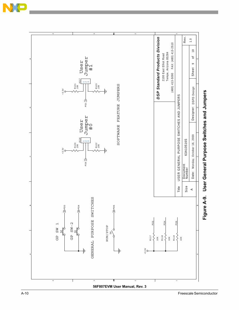
A A
B B
C C
D D
E E
44
33
22
11
GENERAL PURPOSE SWITCHES
GP SW-2
RUN/STOP
GP SW 1
SOFTWARE FEATURE JUMPERS
Jumper
User
#0
Jumper
User
#1
DS
PD
Des
ign
US
ER
GE
NE
RA
L P
UR
PO
SE
SW
ITC
HE
S A
ND
JU
MP
ER
S
63
A1
05
16
S
1.0
918
Mon
day,
Oct
ober
16,
200
0A
DS
P S
tan
dar
d P
rod
uct
s D
ivis
ion
2100
Eas
t E
lliot
Roa
dT
empe
, A
rizo
na 8
5284
Titl
e
Do
cum
en
t
Da
te:
Siz
e
De
sig
ner
:S
he
et
of
Re
v.N
um
be
r
(480
) 41
3-50
90
F
AX
: (4
80)
413-
2510
PD
3
PD
4
PD
5
PD
3
PD
4
PD
5
PD
0P
D1
+3
.3V
+3
.3V
+3
.3V
R1
20
10
K
S4
S5
JG1
6
1 2 3
R1
22
10
K
R1
21
10
KJG
17
1 2 3
R1
23
10
K
R1
17
10
K
R1
18
10
K
R1
19
10
K
S6
56F807EVM User Manual, Rev. 3
A-10 Freescale Semiconductor
Fig
ure
A-9
.
User
Gen
era
l P
urp
ose S
wit
ch
es a
nd
Ju
mp
ers
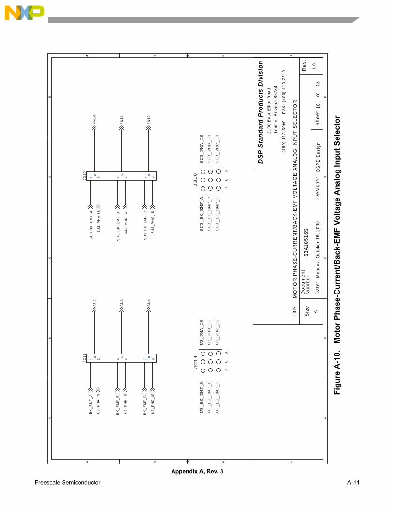
A A
B B
C C
D D
E E
44
33
22
11
U3_BK_EMF_A
U3_BK_EMF_B
U3_BK_EMF_C
U3_PHA_IS
U3_PHB_IS
U3_PHC_IS
89
7
JG14
SU3_BK_EMF_A
SU3_BK_EMF_B
SU3_BK_EMF_C
SU3_PHA_IS
SU3_PHB_IS
SU3_PHC_IS
89
7
JG10
DS
PD
Des
ign
MO
TO
R P
HA
SE
-CU
RR
EN
T/B
AC
K-E
MF
VO
LT
AG
E A
NA
LO
G I
NP
UT
SE
LE
CT
OR
63
A1
05
16
S
1.0
1018
Mon
day,
Oct
ober
16,
200
0A
DS
P S
tan
dar
d P
rod
uct
s D
ivis
ion
2100
Eas
t E
lliot
Roa
dT
empe
, A
rizo
na 8
5284
Titl
e
Do
cum
en
t
Da
te:
Siz
e
De
sig
ner
:S
he
et
of
Re
v.N
um
be
r
(480
) 41
3-50
90
F
AX
: (4
80)
413-
2510
BK
_E
MF
_B
BK
_E
MF
_C
U3
_P
HA
_IS
AN
2
U3
_P
HB
_IS
AN
3
U3
_P
HC
_IS
AN
4
BK
_E
MF
_A
SU
3_
PH
A_
ISA
N1
0
AN
11
AN
12
SU
3_
BK
_E
MF
_A
SU
3_
PH
B_
IS
SU
3_
BK
_E
MF
_C
SU
3_
PH
C_
IS
SU
3_
BK
_E
MF
_B
JG1
4
12
3 4 65 8
7 9
JG1
0
12
3 4 65 8
7 9
Appendix A, Rev. 3
Freescale Semiconductor A-11
Fig
ure
A-1
0. M
oto
r P
hase-C
urr
en
t/B
ack-E
MF
Vo
ltag
e A
nalo
g In
pu
t S
ele
cto
r
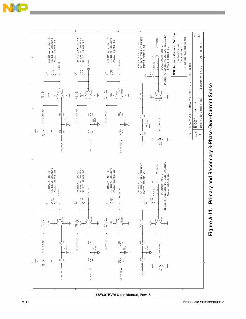
A A
B B
C C
D D
E E
44
33
22
11
PRIMARY UNI-3
PHASE A CURRENT
FAULT SENSE A1
SECONDARY UNI-3
PHASE A CURRENT
FAULT SENSE B1
PRIMARY UNI-3
PHASE B CURRENT
FAULT SENSE A2
PRIMARY UNI-3
PHASE C CURRENT
FAULT SENSE A3
SECONDARY UNI-3
PHASE B CURRENT
FAULT SENSE B2
SECONDARY UNI-3
PHASE C CURRENT
FAULT SENSE B3
PRIMARY UNI-3
DC BUS OVER-CURRENT
FAULT SENSE A1
PRIMARY UNI-3
PHASE A CURRENT/DC BUS CURRENT
FAULT SENSE A1
SECONDARY UNI-3
DC BUS OVER-CURRENT
FAULT SENSE B1
SECONDARY UNI-3
PHASE A CURRENT/DC BUS CURRENT
FAULT SENSE B1
U3_I_S_DCB
DS
PD
Des
ign
PR
IMA
RY
AN
D S
EC
ON
DA
RY
3-P
HA
SE
OV
ER
CU
RR
EN
T S
EN
SE
63A
1051
6S
1.0
1118
Mon
day,
Oct
ober
16,
200
0B
DS
P S
tand
ard
Pro
duct
s D
ivis
ion
2100
Eas
t Elli
ot R
oad
Tem
pe, A
rizon
a 85
284
Title
Doc
umen
t
Dat
e:
Siz
e
Des
igne
r:S
heet
of
Rev
.N
umbe
r
(480
) 41
3-50
90
FAX
: (48
0) 4
13-2
510
S_P
HA
_IS
PR
I_O
VE
R_I
_LIM
IT
P_P
HA
_IS
U3_
I_LI
MIT
_RE
F
U3_
I_LI
MIT
_RE
F
U3_
I_LI
MIT
_RE
F
SU
3_I_
LIM
IT_R
EF
SU
3_I_
LIM
IT_R
EF
SU
3_I_
LIM
IT_R
EF
P_P
HA
_IS
P_O
I_F
AU
LTS
EC
_O
VE
R_I
_LIM
IT
S_P
HA
_IS
S_O
I_F
AU
LT
FA
ULT
A3
FA
ULT
A2
FA
ULT
B3
FA
ULT
B2
AN
1
FA
ULT
A1
U3_
PH
A_I
S
U3_
PH
B_I
S
U3_
PH
C_I
S
SU
3_P
HA
_IS
SU
3_P
HB
_IS
SU
3_P
HC
_IS
AN
9
FA
ULT
B1
+3.3
V
+3.3
V
+3.3
V
+3.3
V
+3.3
V
+3.3
V
+5.0
V+5
.0V
+3.3
V
+5.0
V
+5.0
V+
5.0V
+3.
3V
+5.
0V
+5.0
V+5
.0V
+5.0
V+
5.0V+5
.0V
+5.0
V
R22
5.1K
R20
1M
R14
5.1K
R12
1M
R23
5.1K
R21
1M
R15
5.1K
R13
1M
R5
1M
R7
5.1K
R4
1M
R6
5.1K
R30
1M
R34
5.1K
R28
16K
R29
16K
C15
0.1u
F
JG1
1 2 3
R9
16K
C9
0.1u
F
R8
16K
R17
16K
C11
0.1u
F
R16
16K
C13
0.1u
F
R25
16K
R24 16
K
C10
0.1u
F
R11
16K
R10
16K
R19
16K
R18
16K
C12
0.1u
F
C14
0.1u
F
R26
16K
R27
16K
R33
1M
R35
5.1K
R31
16K
R32
16K
C16
0.1u
F
JG2
1 2 3
+ -
U5B
LM39
3
5 67
8 4
+ -
U4B
LM39
3
5 67
8 4
+ -
U4A
LM39
3
3 21
8 4
+ -
U5A
LM39
3
3 21
8 4
+ -
U3B
LM39
3
5 67
8 4
+ -
U6B
LM39
3
5 67
8 4
+ -
U3A
LM39
3
3 21
8 4
+ -
U6A
LM39
3
3 21
8 4
R2
10K
R3
10K
R37
10K
R36
10K
56F807EVM User Manual, Rev. 3
A-12 Freescale Semiconductor
Fig
ure
A-1
1.
P
rim
ary
an
d S
eco
nd
ary
3-P
hase O
ver-
Cu
rren
t S
en
se
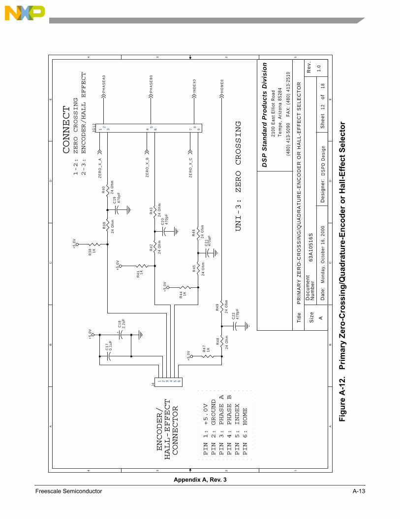
A A
B B
C C
D D
E E
44
33
22
11
HALL-EFFECT
CONNECTOR
UNI-3: ZERO CROSSING
PIN 1: +5.0V
PIN 3: PHASE A
PIN 4: PHASE B
PIN 5: INDEX
PIN 2: GROUND
PIN 6: HOME
CONNECT
1-2: ZERO CROSSING
2-3: ENCODER/HALL EFFECT
ENCODER/
DS
PD
Des
ign
PR
IMA
RY
ZE
RO
-CR
OS
SIN
G/Q
UA
DR
AT
UR
E-E
NC
OD
ER
OR
HA
LL
-EF
FE
CT
SE
LE
CT
OR
63
A1
05
16
S
1.0
1218
Mon
day,
Oct
ober
16,
200
0A
DS
P S
tan
dar
d P
rod
uct
s D
ivis
ion
2100
Eas
t E
lliot
Roa
dT
empe
, A
rizo
na 8
5284
Titl
e
Do
cum
en
t
Da
te:
Siz
e
De
sig
ner
:S
he
et
of
Re
v.N
um
be
r
(480
) 41
3-50
90
F
AX
: (4
80)
413-
2510
HO
ME
0
ZE
RO
_X
_C
ZE
RO
_X
_B
ZE
RO
_X
_A
IND
EX
0
PH
AS
EB
0
PH
AS
EA
0
+5
.0V
+5
.0V
+5
.0V
+5
.0V
+5
.0V
R4
9
24
Oh
m
C2
24
70
pF
R4
8
24
Oh
m
R4
71
K
R4
6
24
Oh
m
R4
5
24
Oh
m
R4
41
K
C2
14
70
pF
R4
3
24
Oh
m
R4
2
24
Oh
m
R4
1 1K
C2
04
70
pF
R3
81
K
C1
94
70
pFR
40
24
Oh
m
R3
9
24
Oh
m+
C1
82
.2u
F
C1
70
.1u
F
J4
1 2 3 4 5 6
JG1
2
12
3 4 65 8
7 9
Appendix A, Rev. 3
Freescale Semiconductor A-13
Fig
ure
A-1
2. P
rim
ary
Zero
-Cro
ssin
g/Q
uad
ratu
re-E
nco
der
or
Hall-E
ffect
Sele
cto
r
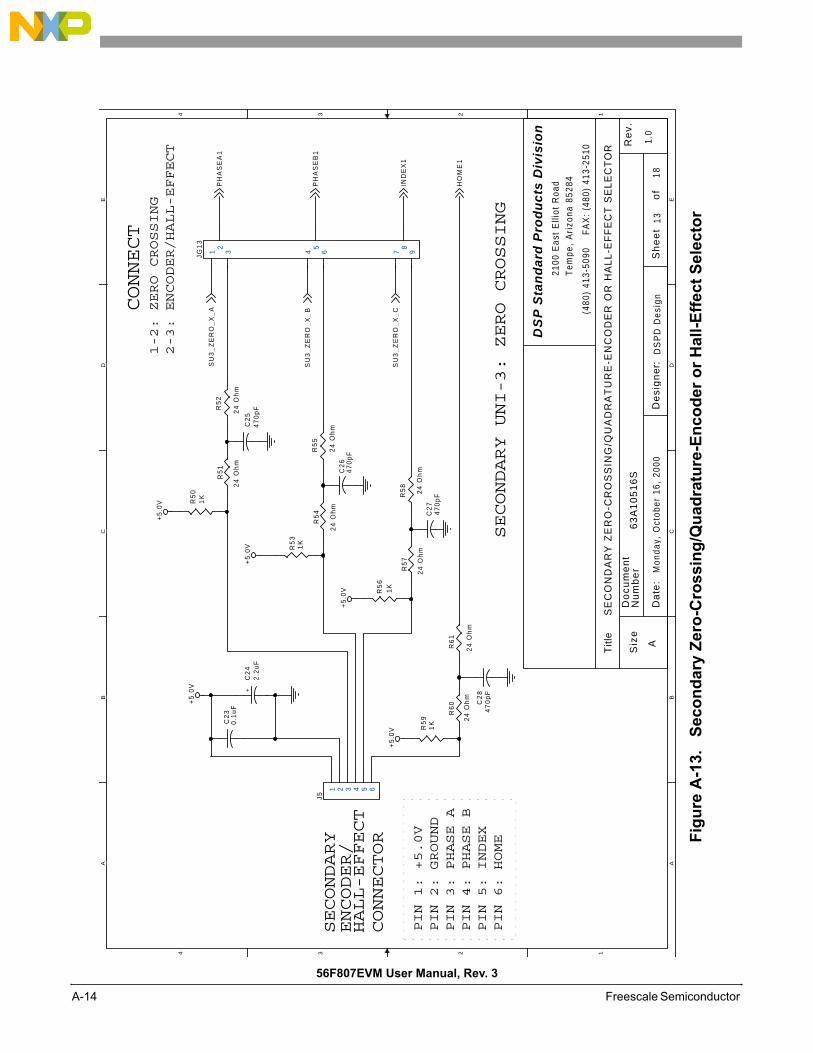
A A
B B
C C
D D
E E
44
33
22
11
ENCODER/
HALL-EFFECT
CONNECTOR
SECONDARY UNI-3: ZERO CROSSING
PIN 1: +5.0V
PIN 3: PHASE A
PIN 4: PHASE B
PIN 5: INDEX
PIN 2: GROUND
PIN 6: HOME
CONNECT
1-2: ZERO CROSSING
2-3: ENCODER/HALL-EFFECT
SECONDARY
DS
PD
Des
ign
SE
CO
ND
AR
Y Z
ER
O-C
RO
SS
ING
/QU
AD
RA
TU
RE
-EN
CO
DE
R O
R H
AL
L-E
FF
EC
T S
EL
EC
TO
R
63
A1
05
16
S1.
013
18M
onda
y, O
ctob
er 1
6, 2
000
A
DS
P S
tan
dar
d P
rod
uct
s D
ivis
ion
2100
Eas
t E
lliot
Roa
dT
empe
, A
rizo
na 8
5284
Titl
e
Do
cum
en
t
Da
te:
Siz
e
De
sig
ner
:S
he
et
of
Re
v.N
um
be
r
(480
) 41
3-50
90
F
AX
: (4
80)
413-
2510
HO
ME
1
SU
3_
ZE
RO
_X
_C
SU
3_
ZE
RO
_X
_B
SU
3_
ZE
RO
_X
_A
PH
AS
EA
1
PH
AS
EB
1
IND
EX
1
+5
.0V
+5
.0V
+5
.0V
+5
.0V
+5
.0V
R5
8
24
Oh
m
R5
7
24
Oh
m
R5
61
K
C2
74
70
pF
R5
5
24
Oh
m
R5
4
24
Oh
m
R5
31
K
C2
64
70
pF
R5
01
K
C2
54
70
pFR
52
24
Oh
m
R5
1
24
Oh
m
+C
24
2.2
uF
C2
30
.1u
F
R6
1
24
Oh
m
C2
84
70
pF
R6
0
24
Oh
m
R5
91
K
J5
1 2 3 4 5 6
JG1
3
12
3 4 65 8
7 9
56F807EVM User Manual, Rev. 3
A-14 Freescale Semiconductor
Fig
ure
A-1
3.
Seco
nd
ary
Zero
-Cro
ssin
g/Q
uad
ratu
re-E
nco
der
or
Hall-E
ffect
Sele
cto
r
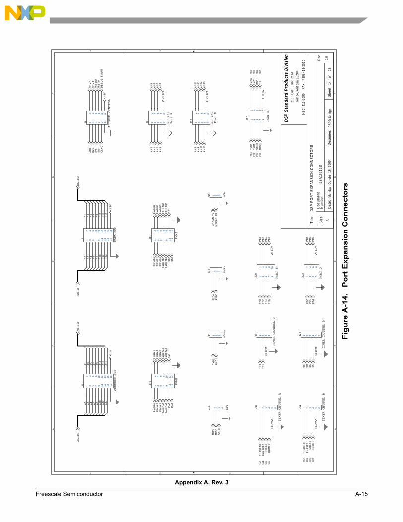
A A
B B
C C
D D
E E
44
33
22
11
PE1
PE3
PE5
PE7
PE0
PE2
PE4
PE6
TB0
TB2
TB3
TB1
TA0
TA2
TA3
TA1
DATA BUS
ADDRESS BUS
SPI
PWM2
SCI1
SCI0
DSP A/D
ADDRESS CONTROL
PORT E
PORT B
PORT D
TIMER CHANNEL C
TIMER CHANNEL D
TIMER CHANNEL B
TIMER CHANNEL A
CAN
DSP A/D
Port A
Port B
PWM1
DS
PD
Des
ign
DS
P P
OR
T E
XP
AN
SIO
N C
ON
NE
CTO
RS
63A
1051
6S
1.0
1418
Mon
day,
Oct
ober
16,
200
0B
DS
P S
tand
ard
Pro
duct
s D
ivis
ion
2100
Eas
t Elli
ot R
oad
Tem
pe, A
rizon
a 85
284
Title
Doc
umen
t
Dat
e:
Siz
e
Des
igne
r:S
heet
of
Rev
.N
umbe
r
(480
) 41
3-50
90
FAX
: (48
0) 4
13-2
510
A0
A2
A4
A6
A8
A10
A12
A14
A1
A3
A5
A7
A9
A11
A13
A15
D0
D2
D4
D6
D8
D10
D12
D14
D1
D3
D5
D7
D9
D11
D13
D15
PB
0P
B2
PB
4P
B6
PB
1P
B3
PB
5P
B7
PD
0P
D2
PD
4
PD
1P
D3
PD
5
/DS
/RS
TO
/IR
QB
/RE
SE
T
/IR
QA
/WR
/RD
/PS
RX
D1
/SS
TXD
0R
XD
0
SC
LKM
ISO
MO
SI
TXD
1
CLK
O
TD
3T
D2
TD
1
TC
0T
C1
DE
BU
G_E
VE
NT
PH
AS
EA
1P
HA
SE
B1
IND
EX
1H
OM
E1
TD
0
PH
AS
EA
0P
HA
SE
B0
IND
EX
0H
OM
E0
AN
0A
N1
AN
2A
N3
AN
4A
N5
AN
6A
N7
A[0
..15
]A
[0..
15]
D[0
..15
]D
[0..
15]
MO
SI
MIS
OS
CLK
TXD
1R
XD
1TX
D0
RX
D0
MS
CA
N_T
XM
SC
AN
_RX
AN
8A
N9
AN
10A
N11
AN
12A
N13
AN
14A
N15
PW
MB
0P
WM
B2
PW
MB
4
PW
MB
1P
WM
B3
PW
MB
5F
AU
LTB
0F
AU
LTB
2F
AU
LTB
1F
AU
LTB
3IS
B0
ISB
2IS
B1
PW
MA
0P
WM
A2
PW
MA
4
PW
MA
1P
WM
A3
PW
MA
5F
AU
LTA
0F
AU
LTA
2F
AU
LTA
1F
AU
LTA
3IS
A0
ISA
2IS
A1 +3
.3V
+3.
3V
+3.
3V
+3.
3V
+3.3
V
+3.
3V+3
.3V
+3.
3VA
+3.
3V
+3.
3V+3
.3V
+3.
3VA
J23
1 3 5 7
2 4 6 8
J20
1 3 5 7 9
2 4 6 8 10
J15 1 2 3
J16 1 2 3
J14 1 2 3
J17
1 3 5 7 9
2 4 6 8 10
J19 1 2 3 4
J18
1 2 3 4 5 6 J21
1 2 3 4 5 6
J9 1 3 5 7 9
2 4 6 8 10
J13 1 2 3 4
J8 1 3 5 7 9 11
2 4 6 8 10 12
J22
1 2 3 4 5 6
J6 12
34
56
78
910
1112
1314
1516
1718
J7 12
34
56
78
910
1112
1314
1516
1718
J12
1 3 5 7 9
2 4 6 8 10
J11
1 3 5 7 9 11 13
2 4 6 8 10 12 14
J10
1 3 5 7 9 11 13
2 4 6 8 10 12 14
Appendix A, Rev. 3
Freescale Semiconductor A-15
Fig
ure
A-1
4. P
ort
Exp
an
sio
n C
on
necto
rs
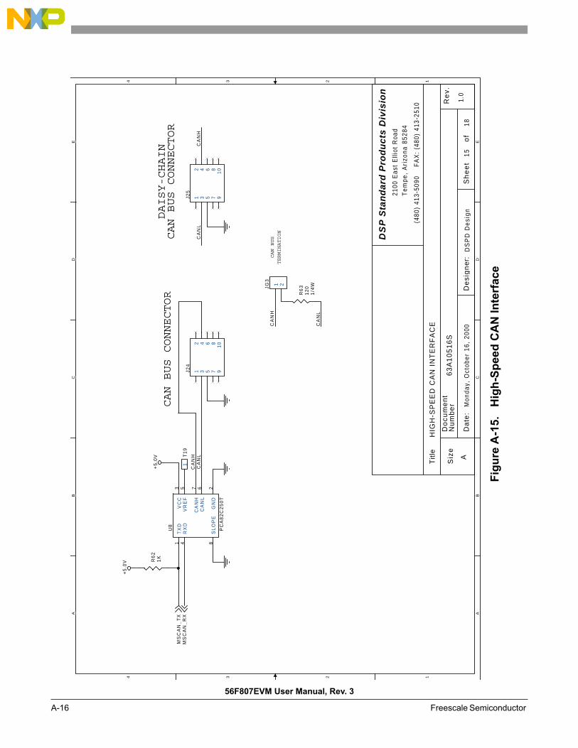
A A
B B
C C
D D
E E
44
33
22
11
CAN BUS CONNECTOR
DAISY-CHAIN
CAN BUS CONNECTOR
CAN BUS
TERMINATION
DS
PD
Des
ign
HIG
H-S
PE
ED
CA
N I
NT
ER
FA
CE
63
A1
05
16
S
1.0
1518
Mon
day,
Oct
ober
16,
200
0A
DS
P S
tan
dar
d P
rod
uct
s D
ivis
ion
2100
Eas
t E
lliot
Roa
dT
empe
, A
rizo
na 8
5284
Titl
e
Do
cum
en
t
Da
te:
Siz
e
De
sig
ner
:S
he
et
of
Re
v.N
um
be
r
(480
) 41
3-50
90
F
AX
: (4
80)
413-
2510
CA
NH
CA
NL
CA
NH
CA
NL
CA
NH
CA
NL
MS
CA
N_
TX
MS
CA
N_
RX
+5
.0V
+5
.0V
J24
1 3 5 7 9
2 4 6 81
0
U8
PC
A8
2C
25
0T
1 4
23 5 67
8
TX
DR
XD
GN
D
VC
CV
RE
F
CA
NL
CA
NH
SL
OP
E
R6
21
K
J25
1 3 5 7 9
2 4 6 81
0
JG3
1 2
R6
31
20
1/4
W
T1
91
56F807EVM User Manual, Rev. 3
A-16 Freescale Semiconductor
Fig
ure
A-1
5.
Hig
h-S
peed
CA
N In
terf
ace
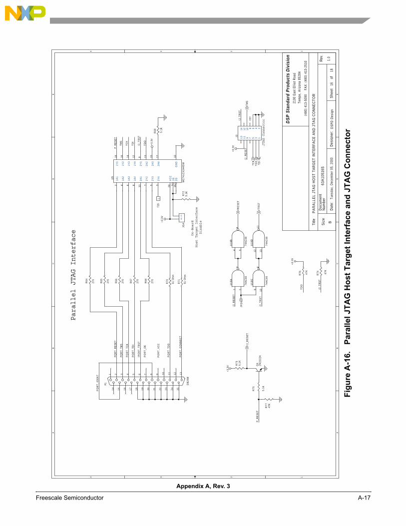
A A
B B
C C
D D
E E
44
33
22
11
Parallel JTAG Interface
KEY
JTAG Connector
On-Board
Host Target Interface
Disable
PO
RT
_VC
C
PO
RT
_DE
DS
PD
Des
ign
PA
RA
LLE
L JT
AG
HO
ST
TAR
GE
T IN
TER
FAC
E A
ND
JTA
G C
ON
NE
CTO
R
63A
1051
6S
1.0
1618
Tues
day,
Dec
embe
r 05
, 200
0B
DS
P S
tand
ard
Pro
duct
s D
ivis
ion
2100
Eas
t Elli
ot R
oad
Tem
pe, A
rizon
a 85
284
Title
Doc
umen
t
Dat
e:
Siz
e
Des
igne
r:S
heet
of
Rev
.N
umbe
r
(480
) 41
3-50
90
FAX
: (48
0) 4
13-2
510
P_R
ES
ET
/J_T
RS
T
/J_R
ES
ET
TD
O
P_R
ES
ET
TMS
TC
K
TD
I
/J_T
RS
T
TD
O
PO
RT
_TD
O
PO
RT
_TM
S
/PO
RT
_TR
ST
PO
RT
_TC
K
PO
RT
_TD
I
PO
RT
_CO
NN
EC
T
PO
RT
_RE
SE
T
PO
RT
_ID
EN
T
/J_T
RS
T
/J_R
ES
ET
/J_T
RS
T
/J_R
ES
ET
TD
IT
DO
TC
K
TMS
/RE
SE
T
/TR
ST
/PO
R
+3.3
V
+3.3
V
+3.3
V
+3.3
V
+3.3
V
R70
51 O
hm
R75
5.1K
R73
5.1K
J3 135791113
2468101214
R77
47K
R76 47
K
R64
270
R66
270
R65
270
R68
270
R67
270
R72
5.1K
JG4
12
U9
MC
74LC
X24
4DW
18 16 14 12 9
7 5 3 1912 4 6 8 11
13 15 17
20
10
1Y1
1Y2
1Y3
1Y4
2Y1
2Y2
2Y3
2Y4
2G1G1A1
1A2
1A3
1A4
2A1
2A2
2A3
2A4
VC
C
GN
D
T20
1R
69 5.1K
P1 DB
25M
1 321514 16
417
518
619
720
821
922
1023
1124
1225
13R
71
51 O
hm
R74 47
K
Q1
2N22
22A
U18
A
74A
C00
1 23
U18
C
74A
C00
9 108
U18
B
74A
C00
4 56
U18
D
74A
C00
12 1311
Appendix A, Rev. 3
Freescale Semiconductor A-17
Fig
ure
A-1
6.
Para
llel JT
AG
Ho
st
Targ
et
Inte
rface a
nd
JT
AG
Co
nn
ecto
r
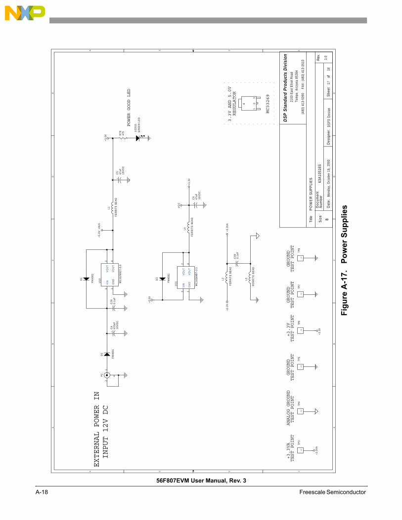
A A
B B
C C
D D
E E
44
33
22
11
EXTERNAL POWER IN
INPUT 12V DC
12
3
4
MC33269
3.3V AND 5.0V
REGULATOR
POWER GOOD LED
+3.3VA
TEST POINT
ANALOG GROUND
TEST POINT
GROUND
TEST POINT
+3.3V
TEST POINT
GROUND
TEST POINT
GROUND
TEST POINT
DS
PD
Des
ign
PO
WE
R S
UP
PLI
ES
63A
1051
6S
1.0
1718
Mon
day,
Oct
ober
16,
200
0B
DS
P S
tand
ard
Pro
duct
s D
ivis
ion
2100
Eas
t Elli
ot R
oad
Tem
pe, A
rizon
a 85
284
Title
Doc
umen
t
Dat
e:
Siz
e
Des
igne
r:S
heet
of
Rev
.N
umbe
r
(480
) 41
3-50
90
FAX
: (48
0) 4
13-2
510
+5.
0V
+3.3
V
+3.3
V
+3.3
VA
+5.0
V
+5.
0V_U
NI3
+3.3
VA
+3.3
V
VC
C
R78
470
P2
1
3
2
C29
0.1u
F
C30
0.1u
F
U11
MC
3326
9DT-
3.3
32 4
1
VIN
VO
UT
VO
UT
GN
DU10
MC
3326
9DT
-5.0
32 4
1
VIN
VO
UT
VO
UT
GN
D
L1
FE
RR
ITE
BE
AD
L3
FE
RR
ITE
BE
AD
L2
FE
RR
ITE
BE
AD
+C
647
uF10
VD
C
+C
447
0uF
16V
DC
+C
547
uF10
VD
C
L4
FE
RR
ITE
BE
AD
TP3
1
TP4
1
TP5
1
TP6
1
TP7
1
TP8
1
D2
FM
4001
D1
FM
4001
LED
10G
RE
EN
LE
D
D3
FM
4001
56F807EVM User Manual, Rev. 3
A-18 Freescale Semiconductor
Fig
ure
A-1
7.
P
ow
er
Su
pp
lie
s
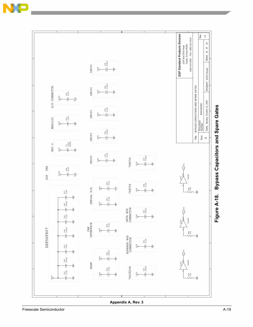
A A
B B
C C
D D
E E
44
33
22
11
DSP56F807
SRAM
A/D CONNECTOR
ADDRESS BUS
CONNECTOR
CONNECTOR
DATA BUS
CAN
INTERFACE
SERIAL D/A
74HC04
74HC04
DSP
VRH
MAX3225
74LCX244
LM393
LM393
LM393
LM393
LM393
UNI-3
DS
PD
Des
ign
BY
PA
SS
CA
PA
CIT
OR
S A
ND
SP
AR
E G
AT
ES
63A
1051
6S
1.0
1818
Mon
day,
Oct
ober
16,
200
0B
DS
P S
tand
ard
Pro
duct
s D
ivis
ion
2100
Eas
t Elli
ot R
oad
Tem
pe, A
rizon
a 85
284
Title
Doc
umen
t
Dat
e:
Siz
e
Des
igne
r:S
heet
of
Rev
.N
umbe
r
(480
) 41
3-50
90
FAX
: (48
0) 4
13-2
510
+3.
3V+3
.3V
+5.
0V+
3.3V
+Vre
f
+3.3
V
+3.3
VA
+3.3
V+3
.3V
+3.3
V
+3.
3VA
+3.3
V
+3.
3V
+5.0
V+5
.0V
+5.0
V+
5.0V
+5.
0V
+3.3
V
+3.3
V
C56
0.1u
FC
550.
01uF
C46
0.01
uFC
500.
1uF
C48
0.1u
F
C54
0.1u
F
C51
0.1u
FC
520.
1uF
R79
5.1k
C53
0.01
uF
C36
0.01
uFC
400.
1uF
C45
0.1u
FC
440.
01uF
C49
0.01
uF
C41
0.1u
F
C35
0.1u
F
U12
D
74A
C04
98
C38
0.1u
F
C34
0.01
uFC
330.
1uF
C32
0.01
uFC
310.
1uF
C57
0.01
uF
C37
0.1u
F
R80
5.1k
U12
E
74A
C04
1110
R81
5.1k
U12
F
74A
C04
1312
C43
0.1u
F
T91
T10
1T1
11
+C
32.
2uF
50V
DC
C39
0.01
uF
Appendix A, Rev. 3
Freescale Semiconductor A-19
Fig
ure
A-1
8.
B
yp
ass C
ap
acit
ors
an
d S
pare
Gate
s

56F807EVM User Manual, Rev. 3
A-20 Freescale Semiconductor
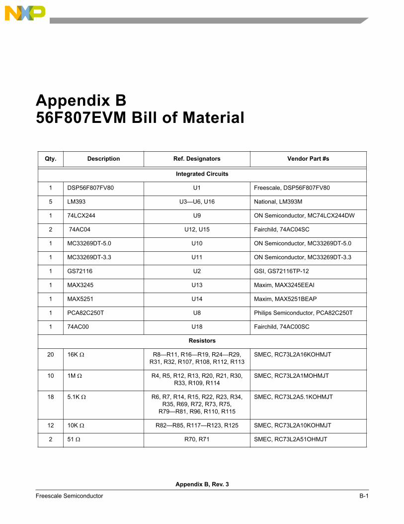
Appendix B, Rev. 3
Freescale Semiconductor B-1
Appendix B56F807EVM Bill of Material
Qty. Description Ref. Designators Vendor Part #s
Integrated Circuits
1 DSP56F807FV80 U1 Freescale, DSP56F807FV80
5 LM393 U3—U6, U16 National, LM393M
1 74LCX244 U9 ON Semiconductor, MC74LCX244DW
2 74AC04 U12, U15 Fairchild, 74AC04SC
1 MC33269DT-5.0 U10 ON Semiconductor, MC33269DT-5.0
1 MC33269DT-3.3 U11 ON Semiconductor, MC33269DT-3.3
1 GS72116 U2 GSI, GS72116TP-12
1 MAX3245 U13 Maxim, MAX3245EEAI
1 MAX5251 U14 Maxim, MAX5251BEAP
1 PCA82C250T U8 Philips Semiconductor, PCA82C250T
1 74AC00 U18 Fairchild, 74AC00SC
Resistors
20 16K R8—R11, R16—R19, R24—R29, R31, R32, R107, R108, R112, R113
SMEC, RC73L2A16KOHMJT
10 1M R4, R5, R12, R13, R20, R21, R30, R33, R109, R114
SMEC, RC73L2A1MOHMJT
18 5.1K R6, R7, R14, R15, R22, R23, R34, R35, R69, R72, R73, R75,
R79—R81, R96, R110, R115
SMEC, RC73L2A5.1KOHMJT
12 10K R82—R85, R117—R123, R125 SMEC, RC73L2A10KOHMJT
2 51 R70, R71 SMEC, RC73L2A51OHMJT
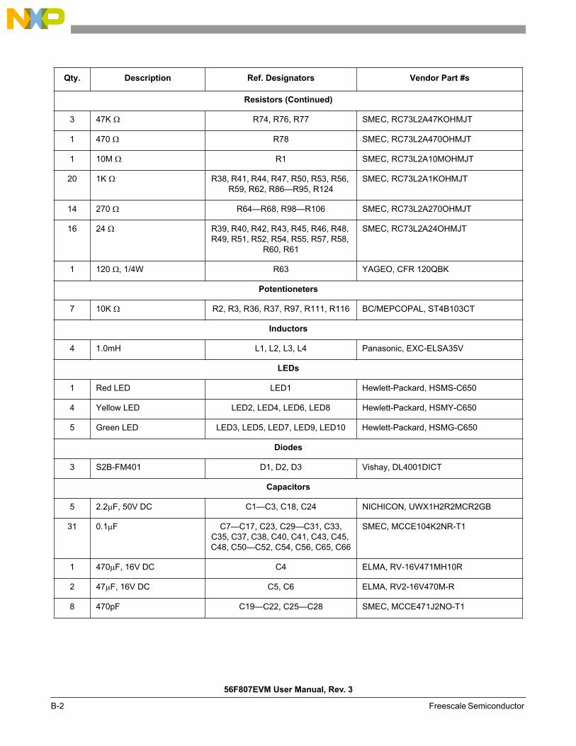
56F807EVM User Manual, Rev. 3
B-2 Freescale Semiconductor
Resistors (Continued)
3 47K R74, R76, R77 SMEC, RC73L2A47KOHMJT
1 470 R78 SMEC, RC73L2A470OHMJT
1 10M R1 SMEC, RC73L2A10MOHMJT
20 1K R38, R41, R44, R47, R50, R53, R56, R59, R62, R86—R95, R124
SMEC, RC73L2A1KOHMJT
14 270 R64—R68, R98—R106 SMEC, RC73L2A270OHMJT
16 24 R39, R40, R42, R43, R45, R46, R48, R49, R51, R52, R54, R55, R57, R58,
R60, R61
SMEC, RC73L2A24OHMJT
1 120 , 1/4W R63 YAGEO, CFR 120QBK
Potentioneters
7 10K R2, R3, R36, R37, R97, R111, R116 BC/MEPCOPAL, ST4B103CT
Inductors
4 1.0mH L1, L2, L3, L4 Panasonic, EXC-ELSA35V
LEDs
1 Red LED LED1 Hewlett-Packard, HSMS-C650
4 Yellow LED LED2, LED4, LED6, LED8 Hewlett-Packard, HSMY-C650
5 Green LED LED3, LED5, LED7, LED9, LED10 Hewlett-Packard, HSMG-C650
Diodes
3 S2B-FM401 D1, D2, D3 Vishay, DL4001DICT
Capacitors
5 2.2 F, 50V DC C1—C3, C18, C24 NICHICON, UWX1H2R2MCR2GB
31 0.1 F C7—C17, C23, C29—C31, C33, C35, C37, C38, C40, C41, C43, C45, C48, C50—C52, C54, C56, C65, C66
SMEC, MCCE104K2NR-T1
1 470 F, 16V DC C4 ELMA, RV-16V471MH10R
2 47 F, 16V DC C5, C6 ELMA, RV2-16V470M-R
8 470pF C19—C22, C25—C28 SMEC, MCCE471J2NO-T1
Qty. Description Ref. Designators Vendor Part #s
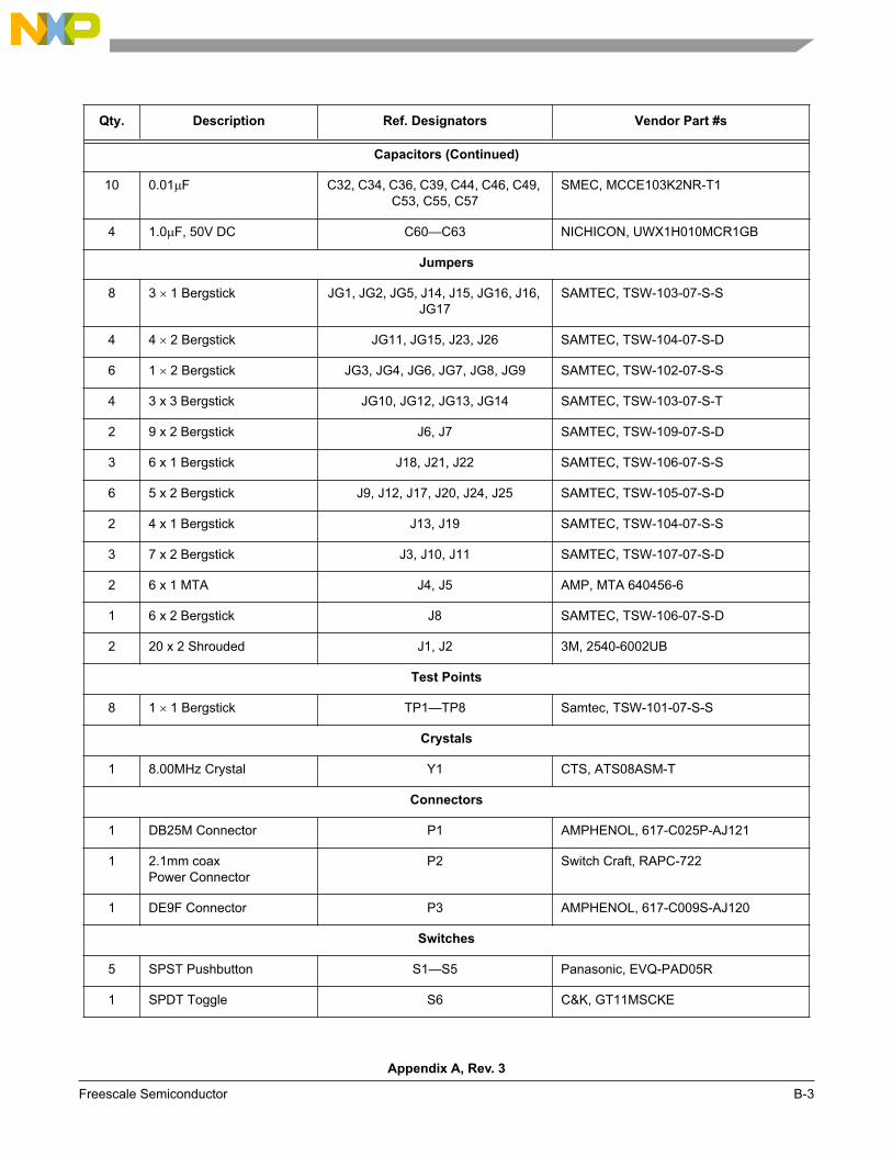
Appendix A, Rev. 3
Freescale Semiconductor B-3
Capacitors (Continued)
10 0.01 F C32, C34, C36, C39, C44, C46, C49, C53, C55, C57
SMEC, MCCE103K2NR-T1
4 1.0 F, 50V DC C60—C63 NICHICON, UWX1H010MCR1GB
Jumpers
8 3 1 Bergstick JG1, JG2, JG5, J14, J15, JG16, J16, JG17
SAMTEC, TSW-103-07-S-S
4 4 2 Bergstick JG11, JG15, J23, J26 SAMTEC, TSW-104-07-S-D
6 1 2 Bergstick JG3, JG4, JG6, JG7, JG8, JG9 SAMTEC, TSW-102-07-S-S
4 3 x 3 Bergstick JG10, JG12, JG13, JG14 SAMTEC, TSW-103-07-S-T
2 9 x 2 Bergstick J6, J7 SAMTEC, TSW-109-07-S-D
3 6 x 1 Bergstick J18, J21, J22 SAMTEC, TSW-106-07-S-S
6 5 x 2 Bergstick J9, J12, J17, J20, J24, J25 SAMTEC, TSW-105-07-S-D
2 4 x 1 Bergstick J13, J19 SAMTEC, TSW-104-07-S-S
3 7 x 2 Bergstick J3, J10, J11 SAMTEC, TSW-107-07-S-D
2 6 x 1 MTA J4, J5 AMP, MTA 640456-6
1 6 x 2 Bergstick J8 SAMTEC, TSW-106-07-S-D
2 20 x 2 Shrouded J1, J2 3M, 2540-6002UB
Test Points
8 1 1 Bergstick TP1—TP8 Samtec, TSW-101-07-S-S
Crystals
1 8.00MHz Crystal Y1 CTS, ATS08ASM-T
Connectors
1 DB25M Connector P1 AMPHENOL, 617-C025P-AJ121
1 2.1mm coaxPower Connector
P2 Switch Craft, RAPC-722
1 DE9F Connector P3 AMPHENOL, 617-C009S-AJ120
Switches
5 SPST Pushbutton S1—S5 Panasonic, EVQ-PAD05R
1 SPDT Toggle S6 C&K, GT11MSCKE
Qty. Description Ref. Designators Vendor Part #s
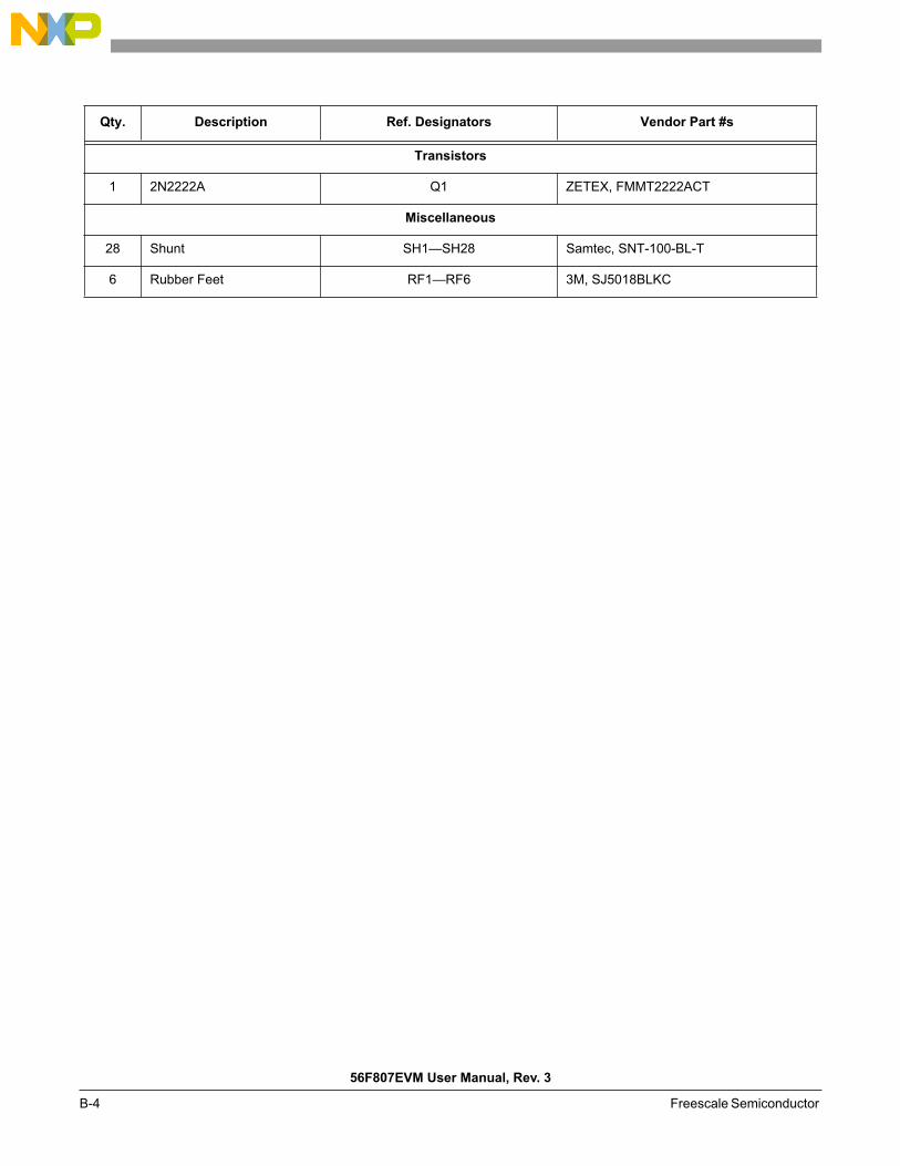
56F807EVM User Manual, Rev. 3
B-4 Freescale Semiconductor
Transistors
1 2N2222A Q1 ZETEX, FMMT2222ACT
Miscellaneous
28 Shunt SH1—SH28 Samtec, SNT-100-BL-T
6 Rubber Feet RF1—RF6 3M, SJ5018BLKC
Qty. Description Ref. Designators Vendor Part #s
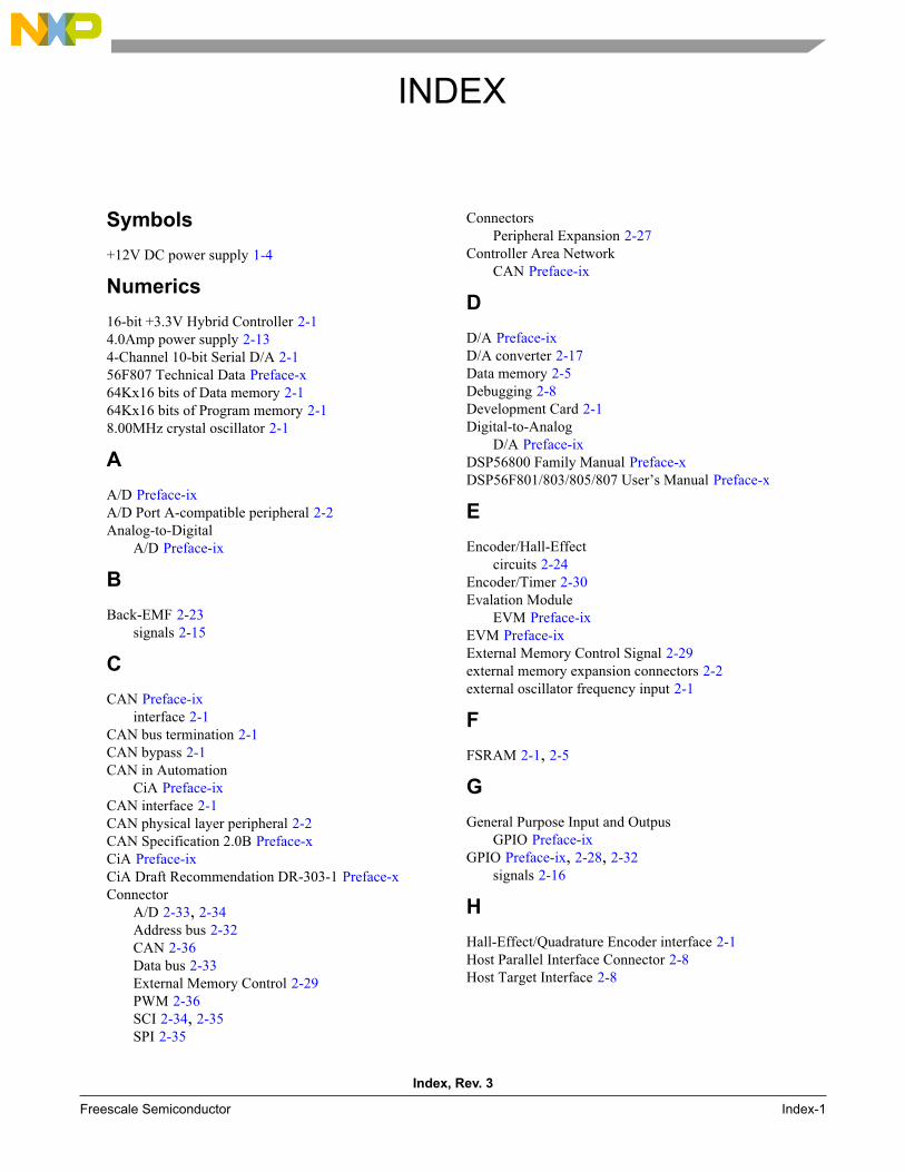
INDEX
Index, Rev. 3
Freescale Semiconductor Index-1
Symbols
+12V DC power supply 1-4
Numerics
16-bit +3.3V Hybrid Controller 2-1
4.0Amp power supply 2-13
4-Channel 10-bit Serial D/A 2-1
56F807 Technical Data Preface-x
64Kx16 bits of Data memory 2-1
64Kx16 bits of Program memory 2-1
8.00MHz crystal oscillator 2-1
A
A/D Preface-ix
A/D Port A-compatible peripheral 2-2
Analog-to-Digital
A/D Preface-ix
B
Back-EMF 2-23
signals 2-15
C
CAN Preface-ix
interface 2-1
CAN bus termination 2-1
CAN bypass 2-1
CAN in Automation
CiA Preface-ix
CAN interface 2-1
CAN physical layer peripheral 2-2
CAN Specification 2.0B Preface-x
CiA Preface-ix
CiA Draft Recommendation DR-303-1 Preface-x
Connector
A/D 2-33, 2-34
Address bus 2-32
CAN 2-36
Data bus 2-33
External Memory Control 2-29
PWM 2-36
SCI 2-34, 2-35
SPI 2-35
Connectors
Peripheral Expansion 2-27
Controller Area Network
CAN Preface-ix
D
D/A Preface-ix
D/A converter 2-17
Data memory 2-5
Debugging 2-8
Development Card 2-1
Digital-to-Analog
D/A Preface-ix
DSP56800 Family Manual Preface-x
DSP56F801/803/805/807 User’s Manual Preface-x
E
Encoder/Hall-Effect
circuits 2-24
Encoder/Timer 2-30
Evalation Module
EVM Preface-ix
EVM Preface-ix
External Memory Control Signal 2-29
external memory expansion connectors 2-2
external oscillator frequency input 2-1
F
FSRAM 2-1, 2-5
G
General Purpose Input and Outpus
GPIO Preface-ix
GPIO Preface-ix, 2-28, 2-32
signals 2-16
H
Hall-Effect/Quadrature Encoder interface 2-1
Host Parallel Interface Connector 2-8
Host Target Interface 2-8
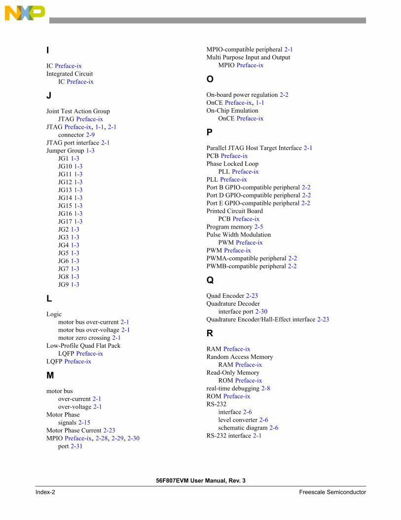
56F807EVM User Manual, Rev. 3
Index-2 Freescale Semiconductor
I
IC Preface-ix
Integrated Circuit
IC Preface-ix
J
Joint Test Action Group
JTAG Preface-ix
JTAG Preface-ix, 1-1, 2-1
connector 2-9
JTAG port interface 2-1
Jumper Group 1-3
JG1 1-3
JG10 1-3
JG11 1-3
JG12 1-3
JG13 1-3
JG14 1-3
JG15 1-3
JG16 1-3
JG17 1-3
JG2 1-3
JG3 1-3
JG4 1-3
JG5 1-3
JG6 1-3
JG7 1-3
JG8 1-3
JG9 1-3
L
Logic
motor bus over-current 2-1
motor bus over-voltage 2-1
motor zero crossing 2-1
Low-Profile Quad Flat Pack
LQFP Preface-ix
LQFP Preface-ix
M
motor bus
over-current 2-1
over-voltage 2-1
Motor Phase
signals 2-15
Motor Phase Current 2-23
MPIO Preface-ix, 2-28, 2-29, 2-30
port 2-31
MPIO-compatible peripheral 2-1
Multi Purpose Input and Output
MPIO Preface-ix
O
On-board power regulation 2-2
OnCE Preface-ix, 1-1
On-Chip Emulation
OnCE Preface-ix
P
Parallel JTAG Host Target Interface 2-1
PCB Preface-ix
Phase Locked Loop
PLL Preface-ix
PLL Preface-ix
Port B GPIO-compatible peripheral 2-2
Port D GPIO-compatible peripheral 2-2
Port E GPIO-compatible peripheral 2-2
Printed Circuit Board
PCB Preface-ix
Program memory 2-5
Pulse Width Modulation
PWM Preface-ix
PWM Preface-ix
PWMA-compatible peripheral 2-2
PWMB-compatible peripheral 2-2
Q
Quad Encoder 2-23
Quadrature Decoder
interface port 2-30
Quadrature Encoder/Hall-Effect interface 2-23
R
RAM Preface-ix
Random Access Memory
RAM Preface-ix
Read-Only Memory
ROM Preface-ix
real-time debugging 2-8
ROM Preface-ix
RS-232
interface 2-6
level converter 2-6
schematic diagram 2-6
RS-232 interface 2-1

Index, Rev. 3
Freescale Semiconductor Index-3
S
SCI Preface-ix
Serial Communications Port 2-34, 2-35
SCI0-compatible peripheral 2-1
SCI1-compatible peripheral 2-2
Serial Communications Interface
SCI Preface-ix
Serial Peripheral Interface
SPI Preface-ix
SPI Preface-ix
Serial Peripheral Interface 2-35
SPI-compatible peripheral 2-2
SRAM Preface-ix
external data 2-1
external program 2-1
Static Random Access Memory
SRAM Preface-ix
T
Timer-compatible peripheral 2-2
U
UART Preface-ix
UNI-3
Back-EMF 2-23
connector/interface 2-14
DC Bus Over-Voltage signal 2-19
Motor Drive interface 2-15
Motor interface
Primary 2-2
Secondary 2-3
Over-Voltage signal 2-21
UNI-3 connector/interface 2-14
Universal Asynchronous Receiver/Transmitter
UART Preface-ix
Z
Zero-Crossing
circuits 2-24


How to Reach Us:
Home Page:www.freescale.com
E-mail:[email protected]
USA/Europe or Locations Not Listed:Freescale SemiconductorTechnical Information Center, CH3701300 N. Alma School RoadChandler, Arizona 85224+1-800-521-6274 or [email protected]
Europe, Middle East, and Africa:Freescale Halbleiter Deutschland GmbHTechnical Information CenterSchatzbogen 781829 Muenchen, Germany+44 1296 380 456 (English)+46 8 52200080 (English)+49 89 92103 559 (German)+33 1 69 35 48 48 (French)[email protected]
Japan:Freescale Semiconductor Japan Ltd.HeadquartersARCO Tower 15F1-8-1, Shimo-Meguro, Meguro-ku,Tokyo 153-0064, Japan0120 191014 or +81 3 5437 [email protected]
Asia/Pacific:Freescale Semiconductor Hong Kong Ltd.Technical Information Center2 Dai King StreetTai Po Industrial EstateTai Po, N.T., Hong Kong+800 2666 [email protected]
For Literature Requests Only:Freescale Semiconductor Literature Distribution CenterP.O. Box 5405Denver, Colorado 802171-800-441-2447 or 303-675-2140Fax: [email protected]
Freescale™ and the Freescale logo are trademarks of Freescale Semiconductor,
Inc. All other product or service names are the property of their respective owners.
This product incorporates SuperFlash® technology licensed from SST.
© Freescale Semiconductor, Inc. 2005. All rights reserved.
DSP56F807EVMUMRev. 307/2005
Information in this document is provided solely to enable system and
software implementers to use Freescale Semiconductor products. There are
no express or implied copyright licenses granted hereunder to design or
fabricate any integrated circuits or integrated circuits based on the
information in this document.
Freescale Semiconductor reserves the right to make changes without further
notice to any products herein. Freescale Semiconductor makes no warranty,
representation or guarantee regarding the suitability of its products for any
particular purpose, nor does Freescale Semiconductor assume any liability
arising out of the application or use of any product or circuit, and specifically
disclaims any and all liability, including without limitation consequential or
incidental damages. “Typical” parameters that may be provided in Freescale
Semiconductor data sheets and/or specifications can and do vary in different
applications and actual performance may vary over time. All operating
parameters, including “Typicals”, must be validated for each customer
application by customer’s technical experts. Freescale Semiconductor does
not convey any license under its patent rights nor the rights of others.
Freescale Semiconductor products are not designed, intended, or authorized
for use as components in systems intended for surgical implant into the body,
or other applications intended to support or sustain life, or for any other
application in which the failure of the Freescale Semiconductor product could
create a situation where personal injury or death may occur. Should Buyer
purchase or use Freescale Semiconductor products for any such unintended
or unauthorized application, Buyer shall indemnify and hold Freescale
Semiconductor and its officers, employees, subsidiaries, affiliates, and
distributors harmless against all claims, costs, damages, and expenses, and
reasonable attorney fees arising out of, directly or indirectly, any claim of
personal injury or death associated with such unintended or unauthorized
use, even if such claim alleges that Freescale Semiconductor was negligent
regarding the design or manufacture of the part.