434 mhz single ended antenna matrix selection … · medium size (wire) helical antenna...
TRANSCRIPT

Rev. 1.1 8/14 Copyright © 2014 by Silicon Laboratories AN849
AN849434 MHZ SINGLE-ENDED ANTENNA MATRIXSELECTION GUIDE
1. IntroductionThis report describes the nine different 50 single-ended antenna types in the easy-to-use 434 MHz AntennaMatrix (WES0070-01-AMS434-01), dedicated to the EZRadio and EZRadioPRO family. Using the developmenttool, readers can test the performance of the Silicon Labs’ RFIC radio family with different types of antennas andfind the best solution for the application in terms of shape, size, cost, and expected range.
The antenna types in the matrix are selected for the most common application areas in the 434 MHz band. Theantennas are optimized and tuned for the antenna PCB + Pico Board + motherboard (MSC-WMB930 WirelessMotherboard) structure (Figure 1).
The input impedance, radiation pattern and antenna gain of every antenna type in the matrix are measured with theabove configuration. The outdoor range is also checked using two identical antenna modules at the two sides ofthe link. The results are given in application note, “AN850: 434 MHz Single-ended Antenna Matrix MeasurementReports”, a separate document containing a detailed measurement report for each antenna type. A brief summaryof antenna gains and measured maximum output ranges can also be found at the end of this report.
In typical customer cases, the antennas are applied without the nearby Pico Board and motherboard and thereforehave no effect. Since all customer applications are different, the right solution may not be found among these fixed-size, fixed-form factor matrix antennas.
For these outlying cases, Silicon Labs recommends modifying or tuning the printed ILA (Inverted L Antenna) andIFA (Inverted F Antenna) types, which are customizable in terms of length and performance. Silicon Labs providesa simple, step-by-step tuning process description in the application note, “AN853: Single-ended Antenna MatrixDesign Guide”. Use this application note to customize and optimize the performance of these antennas.
The current matrix is designed for 50 single-ended solutions. Another matrix will be devoted for the differentialhigh-impedance antennas, which are applied by the Si4010/12/RFIC family.
Figure 1. Typical Measurement Configuration: Antenna Board, Pico Board, and Wireless Motherboard

AN849
2 Rev. 1.1
2. General NotesThe following apply:
EZRadio and EZRadioPRO family of products are supported.
RF Pico Boards equipped with Si4x55, Si4456, or Si446x can be used with these antennas.
RF connectors are matched to 50 .
Boards are equipped with female SMA connectors.Antenna can be connected to the Pico Board using an SMA male-to-male straight adapter.
MSC-WMB930 Wireless Motherboard serves as driving interface of the Pico Board (Figure 1).
The width of the antenna panels is 41 mm. It is identical to the width of the Pico Board and also a typical customer application form factor.
All PCB antennas are designed to 1.55 m-thick FR4 substrate.
3. Antenna Type Description and Typical ApplicationsA picture of the WES0070-01-AMS434-01 915 MHz Antenna Matrix is shown in Figure 2. For the 434 MHz band,eight different PCB antenna solutions are proposed:
Medium Size Printed IFA around the PCB circumference (WES0071-01-APF434M-01)
Ceramic (Chip) Antenna (WES0072-01-ACM434D-01)
Medium Size (Wire) Helical Antenna (WES0074-01-AWH434M-01)
Panic Button IFA (Printed) along the circumference (WES0075-01-APF434P-01)
Panic Button ILA (Printed) along the circumference (WES0076-01-APL434P-01)
Printed Meander Monopole (WES0077-01-APN434D-01)
Small Size Printed ILA (or optional IFA) in dedicated small antenna area (WES0078-01-APL434S-01)
Printed BIFA in a dedicated bigger antenna area (WES0073-01-APB434D-01)
In addition to testing the range of the antennas in the antenna matrix, the range is tested using a commerciallyavailable external whip reference antenna.
Figure 2. WES0070-01-AMS434-01 434 MHz Antenna Matrix Board

AN849
Rev. 1.1 3
3.1. Typical Applications of the Antenna TypesEach antenna type described in this section has advantages and disadvantages relative to context and intendeduse.
3.1.1. Medium Size Printed IFA Around the PCB Circumference (WES0071-01-APF434M-01)This is a low-cost, printed monopole antenna. This type of antenna uses a narrow PCB strip around the PCBcircumference as the antenna area, thereby saving significant space. The drawback can be reduced gain, if theantenna trace is close to the ground metal of the circuitry.
The maximum gain of the realized antenna is ~+0.3 dBi with the antenna PCB + Pico Board + motherboard (MSC-WMB930 Wireless Motherboard) structure. The gain of the antenna board alone has not not measured yet.
This antenna type is sensitive to hand effect, so bench tuning with hand in place is required. But hand effect canalso improve radiation if the hand covers mostly or only the circuit area.
Due to these properties, this antenna type is frequently used in key fobs, where the range requirement is usuallymoderate. The picture of the antenna and the used matching is shown in Figure 3. Fortunately, the antenna isinherently tuned so no external matching elements are required (except the series 0 to connect it in the antennaboard).
Figure 3. Medium Size Printed IFA (WES0071-01-APF434M-01)3.1.2. Ceramic (Chip) Antenna (WES0072-01-ACM434D-01)This type of antenna usually requires a relatively large circuit area with the gaps filled in with ground metal. Thisantenna type is a very good, high-gain, smaller alternative to any printed antenna. However, the cost of the chipantenna is higher. Chip antennas are typically used in set-top boxes and AMRs where the slight additional cost canbe tolerated.
Chip antennas are usually realized on high epsilon dielectric, so the hand effect has less influence on them, unlessthe PCB circuitry area (with ground metal) is small. In these cases, the hand increases the small ground size andthus changes (usually improves) the radiation. Due to this, with small PCB sizes, bench tuning of the impedancewith hand is usually required.
Despite the moderate hand effect sensitivity, chip antennas are not generally used in key fobs due to their relativelyhigher price.
The antenna used in the matrix is the 0433AT62A0020E type from Johanson Technology. With the applied antennaPCB ground size, this antenna requires a two-element external matching network at the input to work at 434 M(see Figure 4). The maximum gain of the realized antenna board is 2.7 dBi with the antenna PCB + Pico Board +motherboard (MSC-WMB930 Wireless Motherboard) structure.

AN849
4 Rev. 1.1
Figure 4. Ceramic Chip Antenna (WES0072-01-ACM434D-01)3.1.3. Medium Size (Wire) Helical Antenna (WES0074-01-AWH434M-01)This type of antenna is a popular, small, low-cost alternative to an external whip antenna. Unfortunately, the gain isslightly lower due to the shorter length. But the gain is usually better than the gain of a small printed antenna (forexample, a small ILA). Typically, this type of antenna is used in key fobs, set-top boxes, AMRs, and alarm systems.In this matrix the ANT-433-HETH type from Linx Technologies, Inc. is selected with a one-element externalmatching (see Figure 5) at the antenna input to tune it to 434 MHz. The maximum of the gain of the realizedantenna board is +3 dBi with the antenna PCB + Pico Board + motherboard (MSC-WMB930 WirelessMotherboard) structure.
The helical monopole is sensitive to hand effect, which is true even if only the circuit (ground) area of the PCB istouched and the ground size is small. As in this case, the ground size around the antenna changes (the radiationusually improves). So with hand effect, further tuning of the matching network is necessary.
Figure 5. Medium Size (Wire) Helical Antenna (WES0074-01-AWH434M-01)
AN849
Rev. 1.1 5
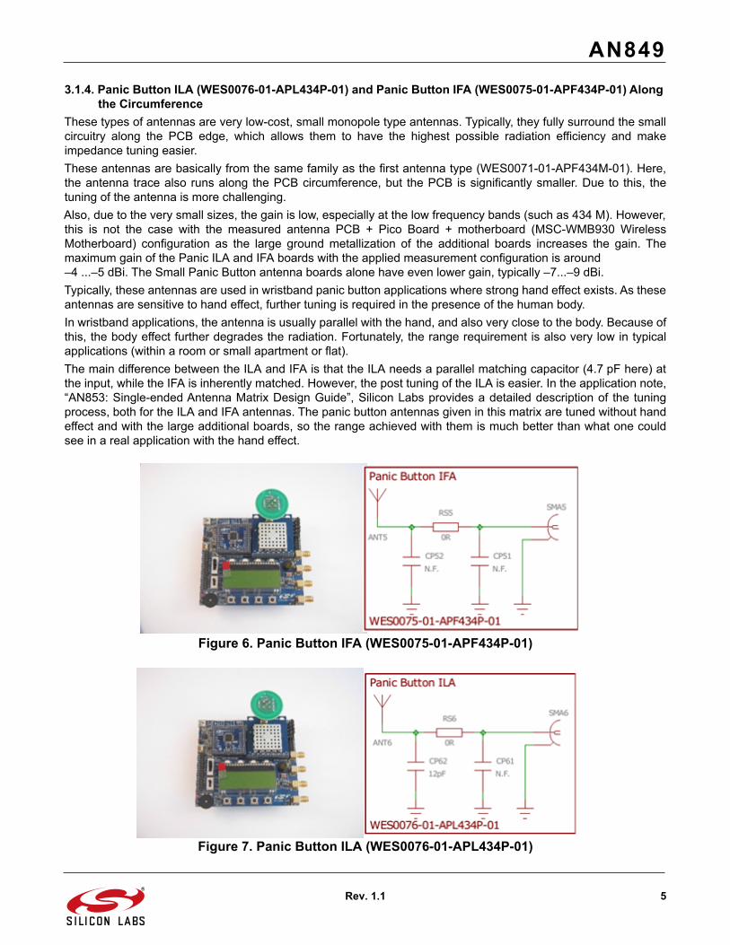
3.1.4. Panic Button ILA (WES0076-01-APL434P-01) and Panic Button IFA (WES0075-01-APF434P-01) Along the Circumference
These types of antennas are very low-cost, small monopole type antennas. Typically, they fully surround the smallcircuitry along the PCB edge, which allows them to have the highest possible radiation efficiency and makeimpedance tuning easier.
These antennas are basically from the same family as the first antenna type (WES0071-01-APF434M-01). Here,the antenna trace also runs along the PCB circumference, but the PCB is significantly smaller. Due to this, thetuning of the antenna is more challenging.
Also, due to the very small sizes, the gain is low, especially at the low frequency bands (such as 434 M). However,this is not the case with the measured antenna PCB + Pico Board + motherboard (MSC-WMB930 WirelessMotherboard) configuration as the large ground metallization of the additional boards increases the gain. Themaximum gain of the Panic ILA and IFA boards with the applied measurement configuration is around –4 ...–5 dBi. The Small Panic Button antenna boards alone have even lower gain, typically –7...–9 dBi.
Typically, these antennas are used in wristband panic button applications where strong hand effect exists. As theseantennas are sensitive to hand effect, further tuning is required in the presence of the human body.
In wristband applications, the antenna is usually parallel with the hand, and also very close to the body. Because ofthis, the body effect further degrades the radiation. Fortunately, the range requirement is also very low in typicalapplications (within a room or small apartment or flat).
The main difference between the ILA and IFA is that the ILA needs a parallel matching capacitor (4.7 pF here) atthe input, while the IFA is inherently matched. However, the post tuning of the ILA is easier. In the application note,“AN853: Single-ended Antenna Matrix Design Guide”, Silicon Labs provides a detailed description of the tuningprocess, both for the ILA and IFA antennas. The panic button antennas given in this matrix are tuned without handeffect and with the large additional boards, so the range achieved with them is much better than what one couldsee in a real application with the hand effect.
Figure 6. Panic Button IFA (WES0075-01-APF434P-01)
Figure 7. Panic Button ILA (WES0076-01-APL434P-01)
AN849
6 Rev. 1.1
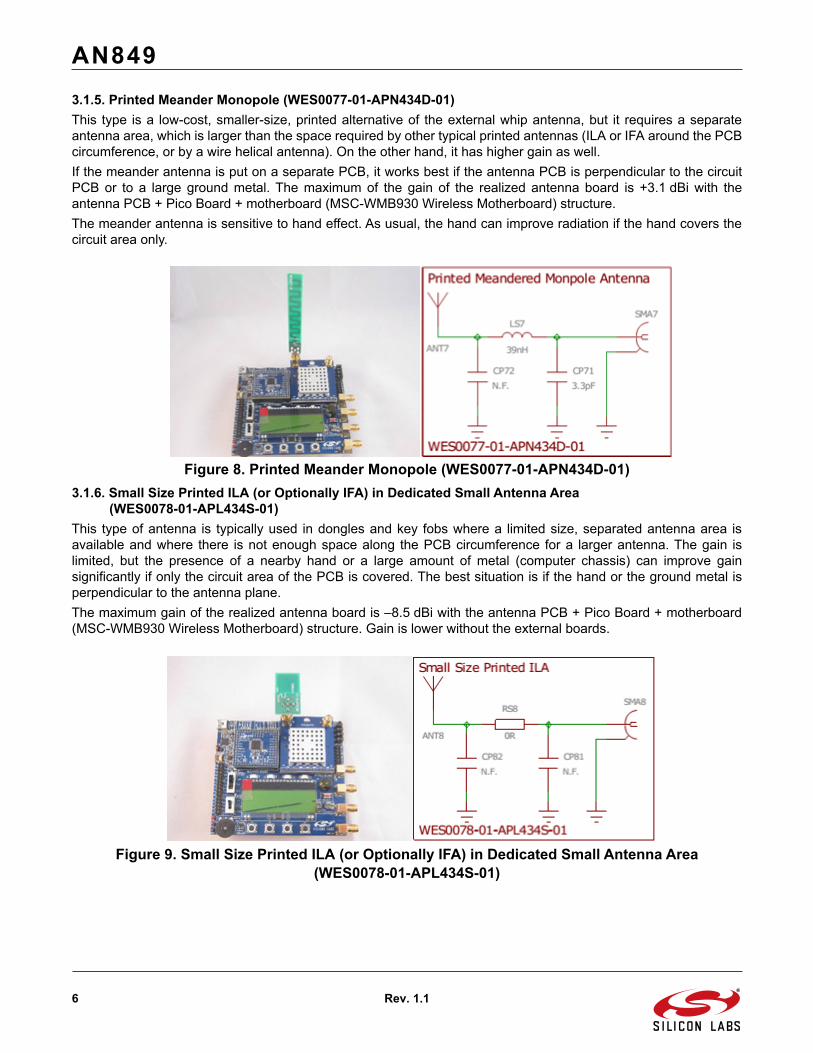
3.1.5. Printed Meander Monopole (WES0077-01-APN434D-01)This type is a low-cost, smaller-size, printed alternative of the external whip antenna, but it requires a separateantenna area, which is larger than the space required by other typical printed antennas (ILA or IFA around the PCBcircumference, or by a wire helical antenna). On the other hand, it has higher gain as well.
If the meander antenna is put on a separate PCB, it works best if the antenna PCB is perpendicular to the circuitPCB or to a large ground metal. The maximum of the gain of the realized antenna board is +3.1 dBi with theantenna PCB + Pico Board + motherboard (MSC-WMB930 Wireless Motherboard) structure.
The meander antenna is sensitive to hand effect. As usual, the hand can improve radiation if the hand covers thecircuit area only.
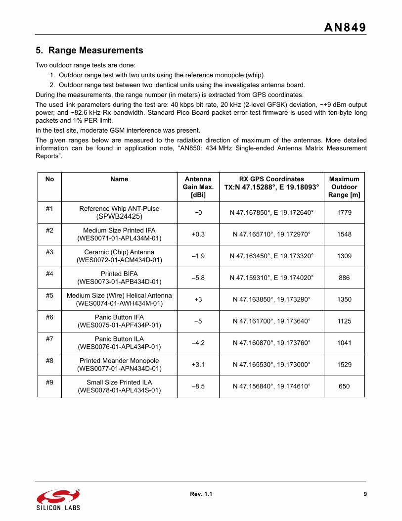
Figure 8. Printed Meander Monopole (WES0077-01-APN434D-01)3.1.6. Small Size Printed ILA (or Optionally IFA) in Dedicated Small Antenna Area
(WES0078-01-APL434S-01)This type of antenna is typically used in dongles and key fobs where a limited size, separated antenna area isavailable and where there is not enough space along the PCB circumference for a larger antenna. The gain islimited, but the presence of a nearby hand or a large amount of metal (computer chassis) can improve gainsignificantly if only the circuit area of the PCB is covered. The best situation is if the hand or the ground metal isperpendicular to the antenna plane.
The maximum gain of the realized antenna board is –8.5 dBi with the antenna PCB + Pico Board + motherboard(MSC-WMB930 Wireless Motherboard) structure. Gain is lower without the external boards.
Figure 9. Small Size Printed ILA (or Optionally IFA) in Dedicated Small Antenna Area(WES0078-01-APL434S-01)

AN849
Rev. 1.1 7
3.1.7. Balanced IFA (BIFA) in Dedicated Bigger Antenna Area (WES0073-01-APB434D-01)The biggest advantage of the BIFA is that the radiation pattern is not much influenced by the PCB ground size andshape, due to the balanced operation of the antenna. (The BIFA antenna is differential and a printed balun is usedat the input to connect it to the 50 single-ended Pico Board input/output.) Due to this, the performance of theBIFA antenna is nearly the same without the Pico Board and motherboard. The maximum gain is –5.8 dBi. TheBIFA antenna mostly radiates to the direction of the antenna’s symmetrical axis; more precisely, it radiates along aplane which includes the symmetrical axis and perpendicular to the antenna PCB.
Unfortunately, the BIFA is sensitive to hand effect if the antenna traces are directly touched. But it is not sensitive ifonly the ground (circuit) part of the PCB is touched.
Figure 10. Balanced IFA (BIFA) (WES0073-01-APB434D-01)

AN849
8 Rev. 1.1
4. Related Documentation:The application note, “AN850: 434 MHz Single-ended Antenna Matrix Measurement Reports”, contains a detaileddescription of each antenna type, including the following:
Antenna match schematic, if it exists
Top and bottom layouts
Picture
Measured impedance
Measured antenna gain
Measured radiation pattern
Harmonic radiation (up to 10th harmonic)
Range measurements
The documentation for each antenna includes a manufacturing pack as well which may be downloaded from therespective web page (www.silabs.com).
AN849
Rev. 1.1 9
5. Range MeasurementsTwo outdoor range tests are done:
1. Outdoor range test with two units using the reference monopole (whip).
2. Outdoor range test between two identical units using the investigates antenna board.
During the measurements, the range number (in meters) is extracted from GPS coordinates.
The used link parameters during the test are: 40 kbps bit rate, 20 kHz (2-level GFSK) deviation, ~+9 dBm outputpower, and ~82.6 kHz Rx bandwidth. Standard Pico Board packet error test firmware is used with ten-byte longpackets and 1% PER limit.
In the test site, moderate GSM interference was present.
The given ranges below are measured to the radiation direction of maximum of the antennas. More detailedinformation can be found in application note, “AN850: 434 MHz Single-ended Antenna Matrix MeasurementReports”.
No Name Antenna Gain Max.
[dBi]
RX GPS CoordinatesTX:N 47.15288°, E 19.18093°
Maximum Outdoor
Range [m]
#1 Reference Whip ANT-Pulse(SPWB24425) ~0 N 47.167850°, E 19.172640° 1779
#2 Medium Size Printed IFA(WES0071-01-APL434M-01)
+0.3 N 47.165710°, 19.172970° 1548
#3 Ceramic (Chip) Antenna (WES0072-01-ACM434D-01)
–1.9 N 47.163450°, E 19.173320° 1309
#4 Printed BIFA (WES0073-01-APB434D-01)
–5.8 N 47.159310°, E 19.174020° 886
#5 Medium Size (Wire) Helical Antenna(WES0074-01-AWH434M-01)
+3 N 47.163850°, 19.173290° 1350
#6 Panic Button IFA(WES0075-01-APF434P-01)
–5 N 47.161700°, 19.173640° 1125
#7 Panic Button ILA (WES0076-01-APL434P-01)
–4.2 N 47.160870°, 19.173760° 1041
#8 Printed Meander Monopole(WES0077-01-APN434D-01)
+3.1 N 47.165530°, 19.173000° 1529
#9 Small Size Printed ILA(WES0078-01-APL434S-01)
–8.5 N 47.156840°, 19.174610° 650

http://www.silabs.com
Silicon Laboratories Inc.400 West Cesar ChavezAustin, TX 78701USA
Smart. Connected. Energy-Friendly.
Productswww.silabs.com/products
Qualitywww.silabs.com/quality
Support and Communitycommunity.silabs.com
DisclaimerSilicon Labs intends to provide customers with the latest, accurate, and in-depth documentation of all peripherals and modules available for system and software implementers using or intending to use the Silicon Labs products. Characterization data, available modules and peripherals, memory sizes and memory addresses refer to each specific device, and "Typical" parameters provided can and do vary in different applications. Application examples described herein are for illustrative purposes only. Silicon Labs reserves the right to make changes without further notice and limitation to product information, specifications, and descriptions herein, and does not give warranties as to the accuracy or completeness of the included information. Silicon Labs shall have no liability for the consequences of use of the information supplied herein. This document does not imply or express copyright licenses granted hereunder to design or fabricate any integrated circuits. The products are not designed or authorized to be used within any Life Support System without the specific written consent of Silicon Labs. A "Life Support System" is any product or system intended to support or sustain life and/or health, which, if it fails, can be reasonably expected to result in significant personal injury or death. Silicon Labs products are not designed or authorized for military applications. Silicon Labs products shall under no circumstances be used in weapons of mass destruction including (but not limited to) nuclear, biological or chemical weapons, or missiles capable of delivering such weapons.
Trademark InformationSilicon Laboratories Inc.® , Silicon Laboratories®, Silicon Labs®, SiLabs® and the Silicon Labs logo®, Bluegiga®, Bluegiga Logo®, Clockbuilder®, CMEMS®, DSPLL®, EFM®, EFM32®, EFR, Ember®, Energy Micro, Energy Micro logo and combinations thereof, "the world’s most energy friendly microcontrollers", Ember®, EZLink®, EZRadio®, EZRadioPRO®, Gecko®, ISOmodem®, Precision32®, ProSLIC®, Simplicity Studio®, SiPHY®, Telegesis, the Telegesis Logo®, USBXpress® and others are trademarks or registered trademarks of Silicon Labs. ARM, CORTEX, Cortex-M3 and THUMB are trademarks or registered trademarks of ARM Holdings. Keil is a registered trademark of ARM Limited. All other products or brand names mentioned herein are trademarks of their respective holders.