4 mbit, low voltage, page-erasable serial flash...
TRANSCRIPT
1/37
PRELIMINARY DATA
January 2005This is preliminary information on a new product now in development or undergoing evaluation. Details are subject to change without notice.
M25PE404 Mbit, Low Voltage, Page-Erasable Serial Flash Memory with
Byte-Alterability, 25 MHz SPI Bus, Standard Pinout
FEATURES SUMMARY Industrial Standard SPI Pinout 4Mbit of Page-Erasable Flash Memory Page Write (up to 256 Bytes) in 11ms (typical) Page Program (up to 256 Bytes) in 1.2ms
(typical) Page Erase (256 Bytes) in 10ms (typical) Sector Erase (512 Kbit) 2.7 to 3.6V Single Supply Voltage SPI Bus Compatible Serial Interface 25MHz Clock Rate (maximum) Deep Power-down Mode 1µA (typical) Electronic Signature
– JEDEC Standard Two-Byte Signature (8013h)
More than 100,000 Write Cycles More than 20 Year Data Retention Hardware Write Protection of the Top Sector
(64KB)
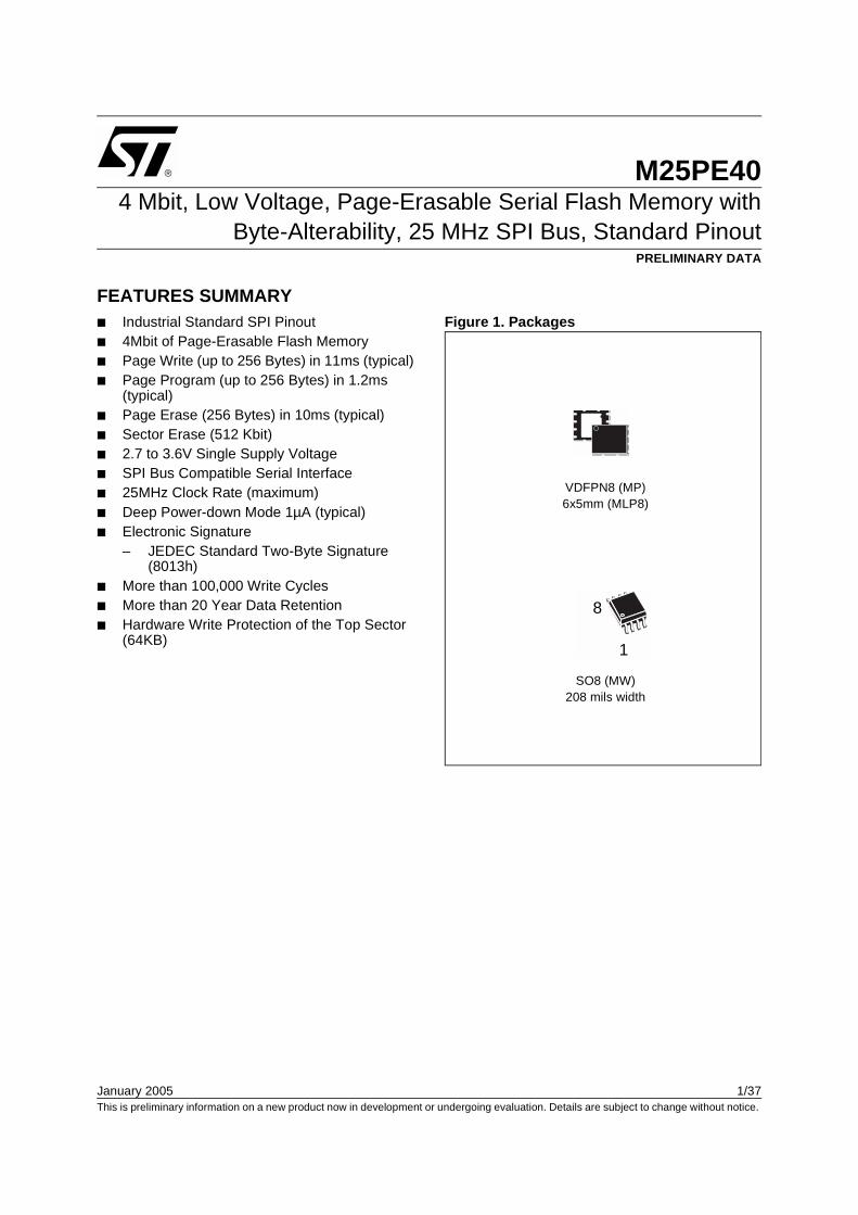
Figure 1. Packages
VDFPN8 (MP)6x5mm (MLP8)
8
1
SO8 (MW)208 mils width
M25PE40
2/37
TABLE OF CONTENTS
FEATURES SUMMARY . . . . . . . . . . . . . . . . . . . . . . . . . . . . . . . . . . . . . . . . . . . . . . . . . . . . . . . . . . . . . 1
Figure 1. Packages . . . . . . . . . . . . . . . . . . . . . . . . . . . . . . . . . . . . . . . . . . . . . . . . . . . . . . . . . . . . . . 1Figure 2. Logic Diagram . . . . . . . . . . . . . . . . . . . . . . . . . . . . . . . . . . . . . . . . . . . . . . . . . . . . . . . . . . 5Table 1. Signal Names . . . . . . . . . . . . . . . . . . . . . . . . . . . . . . . . . . . . . . . . . . . . . . . . . . . . . . . . . . 5Figure 3. VDFPN and SO Connections . . . . . . . . . . . . . . . . . . . . . . . . . . . . . . . . . . . . . . . . . . . . . . 5
SIGNAL DESCRIPTION . . . . . . . . . . . . . . . . . . . . . . . . . . . . . . . . . . . . . . . . . . . . . . . . . . . . . . . . . . . . . 6
Serial Data Output (Q). . . . . . . . . . . . . . . . . . . . . . . . . . . . . . . . . . . . . . . . . . . . . . . . . . . . . . . . . . . . 6Serial Data Input (D) . . . . . . . . . . . . . . . . . . . . . . . . . . . . . . . . . . . . . . . . . . . . . . . . . . . . . . . . . . . . . 6Serial Clock (C) . . . . . . . . . . . . . . . . . . . . . . . . . . . . . . . . . . . . . . . . . . . . . . . . . . . . . . . . . . . . . . . . . 6Chip Select (S) . . . . . . . . . . . . . . . . . . . . . . . . . . . . . . . . . . . . . . . . . . . . . . . . . . . . . . . . . . . . . . . . . 6Reset (Reset) . . . . . . . . . . . . . . . . . . . . . . . . . . . . . . . . . . . . . . . . . . . . . . . . . . . . . . . . . . . . . . . . . . 6Top Sector Lock (TSL) . . . . . . . . . . . . . . . . . . . . . . . . . . . . . . . . . . . . . . . . . . . . . . . . . . . . . . . . . . . 6
SPI MODES . . . . . . . . . . . . . . . . . . . . . . . . . . . . . . . . . . . . . . . . . . . . . . . . . . . . . . . . . . . . . . . . . . . . . . . 7
Figure 4. Bus Master and Memory Devices on the SPI Bus. . . . . . . . . . . . . . . . . . . . . . . . . . . . . . . 7Figure 5. SPI Modes Supported . . . . . . . . . . . . . . . . . . . . . . . . . . . . . . . . . . . . . . . . . . . . . . . . . . . . 7
OPERATING FEATURES . . . . . . . . . . . . . . . . . . . . . . . . . . . . . . . . . . . . . . . . . . . . . . . . . . . . . . . . . . . . 8
Sharing the Overhead of Modifying Data . . . . . . . . . . . . . . . . . . . . . . . . . . . . . . . . . . . . . . . . . . . 8An Easy Way to Modify Data . . . . . . . . . . . . . . . . . . . . . . . . . . . . . . . . . . . . . . . . . . . . . . . . . . . . . 8A Fast Way to Modify Data . . . . . . . . . . . . . . . . . . . . . . . . . . . . . . . . . . . . . . . . . . . . . . . . . . . . . . . 8Polling During a Write, Program or Erase Cycle . . . . . . . . . . . . . . . . . . . . . . . . . . . . . . . . . . . . . 8Reset. . . . . . . . . . . . . . . . . . . . . . . . . . . . . . . . . . . . . . . . . . . . . . . . . . . . . . . . . . . . . . . . . . . . . . . . . 8Active Power, Standby Power and Deep Power-Down Modes . . . . . . . . . . . . . . . . . . . . . . . . . . 8Status Register . . . . . . . . . . . . . . . . . . . . . . . . . . . . . . . . . . . . . . . . . . . . . . . . . . . . . . . . . . . . . . . . 9WIP bit . . . . . . . . . . . . . . . . . . . . . . . . . . . . . . . . . . . . . . . . . . . . . . . . . . . . . . . . . . . . . . . . . . . . . . . . 9WEL bit . . . . . . . . . . . . . . . . . . . . . . . . . . . . . . . . . . . . . . . . . . . . . . . . . . . . . . . . . . . . . . . . . . . . . . . 9Table 2. Status Register Format . . . . . . . . . . . . . . . . . . . . . . . . . . . . . . . . . . . . . . . . . . . . . . . . . . . 9Protection Modes . . . . . . . . . . . . . . . . . . . . . . . . . . . . . . . . . . . . . . . . . . . . . . . . . . . . . . . . . . . . . . 9
MEMORY ORGANIZATION . . . . . . . . . . . . . . . . . . . . . . . . . . . . . . . . . . . . . . . . . . . . . . . . . . . . . . . . . 10
Table 3. Memory Organization . . . . . . . . . . . . . . . . . . . . . . . . . . . . . . . . . . . . . . . . . . . . . . . . . . . 10Figure 6. Block Diagram . . . . . . . . . . . . . . . . . . . . . . . . . . . . . . . . . . . . . . . . . . . . . . . . . . . . . . . . . 11
INSTRUCTIONS . . . . . . . . . . . . . . . . . . . . . . . . . . . . . . . . . . . . . . . . . . . . . . . . . . . . . . . . . . . . . . . . . . 12
Table 4. Instruction Set . . . . . . . . . . . . . . . . . . . . . . . . . . . . . . . . . . . . . . . . . . . . . . . . . . . . . . . . . 12Write Enable (WREN) . . . . . . . . . . . . . . . . . . . . . . . . . . . . . . . . . . . . . . . . . . . . . . . . . . . . . . . . . . 13Figure 7. Write Enable (WREN) Instruction Sequence . . . . . . . . . . . . . . . . . . . . . . . . . . . . . . . . . . 13Write Disable (WRDI). . . . . . . . . . . . . . . . . . . . . . . . . . . . . . . . . . . . . . . . . . . . . . . . . . . . . . . . . . . 13Figure 8. Write Disable (WRDI) Instruction Sequence . . . . . . . . . . . . . . . . . . . . . . . . . . . . . . . . . . 13Read Identification (RDID) . . . . . . . . . . . . . . . . . . . . . . . . . . . . . . . . . . . . . . . . . . . . . . . . . . . . . . 14Table 5. Read Identification (RDID) Data-Out Sequence . . . . . . . . . . . . . . . . . . . . . . . . . . . . . . . 14
3/37
M25PE40
Figure 9. Read Identification (RDID) Instruction Sequence and Data-Out Sequence . . . . . . . . . . 14Read Status Register (RDSR). . . . . . . . . . . . . . . . . . . . . . . . . . . . . . . . . . . . . . . . . . . . . . . . . . . . 15WIP bit . . . . . . . . . . . . . . . . . . . . . . . . . . . . . . . . . . . . . . . . . . . . . . . . . . . . . . . . . . . . . . . . . . . . . . . 15WEL bit . . . . . . . . . . . . . . . . . . . . . . . . . . . . . . . . . . . . . . . . . . . . . . . . . . . . . . . . . . . . . . . . . . . . . . 15Figure 10.Read Status Register (RDSR) Instruction Sequence and Data-Out Sequence . . . . . . . 15Read Data Bytes (READ). . . . . . . . . . . . . . . . . . . . . . . . . . . . . . . . . . . . . . . . . . . . . . . . . . . . . . . . 16Figure 11.Read Data Bytes (READ) Instruction Sequence and Data-Out Sequence . . . . . . . . . . . 16Read Data Bytes at Higher Speed (FAST_READ). . . . . . . . . . . . . . . . . . . . . . . . . . . . . . . . . . . . 17Figure 12.Read Data Bytes at Higher Speed (FAST_READ) Instruction Sequence
and Data-Out Sequence . . . . . . . . . . . . . . . . . . . . . . . . . . . . . . . . . . . . . . . . . . . . . . . . . 17Page Write (PW). . . . . . . . . . . . . . . . . . . . . . . . . . . . . . . . . . . . . . . . . . . . . . . . . . . . . . . . . . . . . . . 18Figure 13.Page Write (PW) Instruction Sequence. . . . . . . . . . . . . . . . . . . . . . . . . . . . . . . . . . . . . . 18Page Program (PP) . . . . . . . . . . . . . . . . . . . . . . . . . . . . . . . . . . . . . . . . . . . . . . . . . . . . . . . . . . . . 19Figure 14.Page Program (PP) Instruction Sequence . . . . . . . . . . . . . . . . . . . . . . . . . . . . . . . . . . . 19Page Erase (PE) . . . . . . . . . . . . . . . . . . . . . . . . . . . . . . . . . . . . . . . . . . . . . . . . . . . . . . . . . . . . . . . 20Figure 15.Page Erase (PE) Instruction Sequence. . . . . . . . . . . . . . . . . . . . . . . . . . . . . . . . . . . . . . 20Sector Erase (SE) . . . . . . . . . . . . . . . . . . . . . . . . . . . . . . . . . . . . . . . . . . . . . . . . . . . . . . . . . . . . . 21Figure 16.Sector Erase (SE) Instruction Sequence. . . . . . . . . . . . . . . . . . . . . . . . . . . . . . . . . . . . . 21Deep Power-down (DP) . . . . . . . . . . . . . . . . . . . . . . . . . . . . . . . . . . . . . . . . . . . . . . . . . . . . . . . . . 22Figure 17.Deep Power-down (DP) Instruction Sequence . . . . . . . . . . . . . . . . . . . . . . . . . . . . . . . . 22Release from Deep Power-down (RDP). . . . . . . . . . . . . . . . . . . . . . . . . . . . . . . . . . . . . . . . . . . . 23Figure 18.Release from Deep Power-down (RDP) Instruction Sequence. . . . . . . . . . . . . . . . . . . . 23
POWER-UP AND POWER-DOWN . . . . . . . . . . . . . . . . . . . . . . . . . . . . . . . . . . . . . . . . . . . . . . . . . . . . 24
Figure 19.Power-up Timing . . . . . . . . . . . . . . . . . . . . . . . . . . . . . . . . . . . . . . . . . . . . . . . . . . . . . . . 24Table 6. Power-Up Timing and VWI Threshold . . . . . . . . . . . . . . . . . . . . . . . . . . . . . . . . . . . . . . . 25
INITIAL DELIVERY STATE. . . . . . . . . . . . . . . . . . . . . . . . . . . . . . . . . . . . . . . . . . . . . . . . . . . . . . . . . . 25
MAXIMUM RATING. . . . . . . . . . . . . . . . . . . . . . . . . . . . . . . . . . . . . . . . . . . . . . . . . . . . . . . . . . . . . . . . 26
Table 7. Absolute Maximum Ratings . . . . . . . . . . . . . . . . . . . . . . . . . . . . . . . . . . . . . . . . . . . . . . . 26
DC and AC PARAMETERS . . . . . . . . . . . . . . . . . . . . . . . . . . . . . . . . . . . . . . . . . . . . . . . . . . . . . . . . . 27
Table 8. Operating Conditions. . . . . . . . . . . . . . . . . . . . . . . . . . . . . . . . . . . . . . . . . . . . . . . . . . . . 27Table 9. AC Measurement Conditions. . . . . . . . . . . . . . . . . . . . . . . . . . . . . . . . . . . . . . . . . . . . . . 27Figure 20.AC Measurement I/O Waveform . . . . . . . . . . . . . . . . . . . . . . . . . . . . . . . . . . . . . . . . . . . 27Table 10. Capacitance. . . . . . . . . . . . . . . . . . . . . . . . . . . . . . . . . . . . . . . . . . . . . . . . . . . . . . . . . . . 27Table 11. DC Characteristics. . . . . . . . . . . . . . . . . . . . . . . . . . . . . . . . . . . . . . . . . . . . . . . . . . . . . . 28Table 12. AC Characteristics . . . . . . . . . . . . . . . . . . . . . . . . . . . . . . . . . . . . . . . . . . . . . . . . . . . . . . 29Figure 21.Serial Input Timing . . . . . . . . . . . . . . . . . . . . . . . . . . . . . . . . . . . . . . . . . . . . . . . . . . . . . 30Figure 22.Top Sector Lock Setup and Hold Timing. . . . . . . . . . . . . . . . . . . . . . . . . . . . . . . . . . . . . 30Figure 23.Output Timing . . . . . . . . . . . . . . . . . . . . . . . . . . . . . . . . . . . . . . . . . . . . . . . . . . . . . . . . . 31Table 13. Reset Timings . . . . . . . . . . . . . . . . . . . . . . . . . . . . . . . . . . . . . . . . . . . . . . . . . . . . . . . . . 32Figure 24.Reset AC Waveforms . . . . . . . . . . . . . . . . . . . . . . . . . . . . . . . . . . . . . . . . . . . . . . . . . . . 32
PACKAGE MECHANICAL . . . . . . . . . . . . . . . . . . . . . . . . . . . . . . . . . . . . . . . . . . . . . . . . . . . . . . . . . . 33
M25PE40
4/37
Figure 25.MLP8, 8-lead Very thin Dual Flat Package No lead, 6x5mm, Package Outline . . . . . . . 33Table 14. MLP8, 8-lead Very thin Dual Flat Package No lead, 6x5mm,
Package Mechanical Data . . . . . . . . . . . . . . . . . . . . . . . . . . . . . . . . . . . . . . . . . . . . . . . . 33Figure 26.SO8 wide – 8 lead Plastic Small Outline, 208 mils body width, Package Outline . . . . . . 34Table 15. SO8 wide – 8 lead Plastic Small Outline, 208 mils body width, Mechanical Data . . . . . . 34
PART NUMBERING . . . . . . . . . . . . . . . . . . . . . . . . . . . . . . . . . . . . . . . . . . . . . . . . . . . . . . . . . . . . . . . 35
Table 16. Ordering Information Scheme . . . . . . . . . . . . . . . . . . . . . . . . . . . . . . . . . . . . . . . . . . . . . 35
REVISION HISTORY. . . . . . . . . . . . . . . . . . . . . . . . . . . . . . . . . . . . . . . . . . . . . . . . . . . . . . . . . . . . . . . 36
Table 17. Document Revision History . . . . . . . . . . . . . . . . . . . . . . . . . . . . . . . . . . . . . . . . . . . . . . . 36
5/37
M25PE40
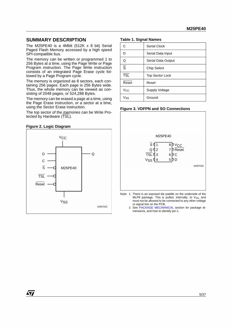
SUMMARY DESCRIPTIONThe M25PE40 is a 4Mbit (512K x 8 bit) SerialPaged Flash Memory accessed by a high speedSPI-compatible bus.The memory can be written or programmed 1 to256 Bytes at a time, using the Page Write or PageProgram instruction. The Page Write instructionconsists of an integrated Page Erase cycle fol-lowed by a Page Program cycle.The memory is organized as 8 sectors, each con-taining 256 pages. Each page is 256 Bytes wide.Thus, the whole memory can be viewed as con-sisting of 2048 pages, or 524,288 Bytes.The memory can be erased a page at a time, usingthe Page Erase instruction, or a sector at a time,using the Sector Erase instruction.The top sector of the memories can be Write Pro-tected by Hardware (TSL).
Figure 2. Logic Diagram
Table 1. Signal Names
Figure 3. VDFPN and SO Connections
Note: 1. There is an exposed die paddle on the underside of theMLP8 package. This is pulled, internally, to VSS, andmust not be allowed to be connected to any other voltageor signal line on the PCB.
2. See PACKAGE MECHANICAL section for package di-mensions, and how to identify pin-1.
Reset
AI09704C
S
VCC
M25PE40
VSS
TSL
Q
C
D
C Serial Clock
D Serial Data Input
Q Serial Data Output
S Chip Select
TSL Top Sector Lock
Reset Reset
VCC Supply Voltage
VSS Ground
1
AI09703C
234
8765 DVSS
CResetQ
S VCC
TSL
M25PE40
M25PE40
6/37
SIGNAL DESCRIPTION
Serial Data Output (Q). This output signal isused to transfer data serially out of the device.Data is shifted out on the falling edge of SerialClock (C).
Serial Data Input (D). This input signal is used totransfer data serially into the device. It receives in-structions, addresses, and the data to be pro-grammed. Values are latched on the rising edge ofSerial Clock (C).
Serial Clock (C). This input signal provides thetiming of the serial interface. Instructions, address-es, or data present at Serial Data Input (D) arelatched on the rising edge of Serial Clock (C). Dataon Serial Data Output (Q) changes after the fallingedge of Serial Clock (C).
Chip Select (S). When this input signal is High,the device is deselected and Serial Data Output(Q) is at high impedance. Unless an internal Read,Program, Erase or Write cycle is in progress, thedevice will be in the Standby Power mode (this isnot the Deep Power-down mode). Driving Chip
Select (S) Low selects the device, placing it in theActive Power mode.After Power-up, a falling edge on Chip Select (S)is required prior to the start of any instruction.
Reset (Reset). The Reset (Reset) input providesa hardware reset for the memory.When Reset (Reset) is driven High, the memory isin the normal operating mode. When Reset (Re-set) is driven Low, the memory will enter the Resetmode. In this mode, the output is high impedance.Driving Reset (Reset) Low while an internal oper-ation is in progress will affect this operation (write,program or erase cycle) and data may be lost.
Top Sector Lock (TSL). This input signal putsthe device in the Hardware Protected mode, whenTop Sector Lock (TSL) is connected to VSS, caus-ing the top 256 pages (upper addresses) of thememory to become read-only (protected fromwrite, program and erase operations).When Top Sector Lock (TSL) is connected to VCC,the top 256 pages of memory behave like the otherpages of memory.
7/37
M25PE40
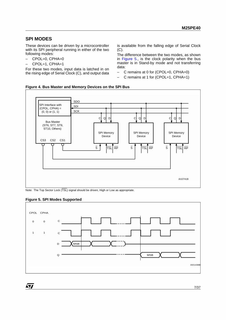
SPI MODESThese devices can be driven by a microcontrollerwith its SPI peripheral running in either of the twofollowing modes:– CPOL=0, CPHA=0– CPOL=1, CPHA=1For these two modes, input data is latched in onthe rising edge of Serial Clock (C), and output data
is available from the falling edge of Serial Clock(C).The difference between the two modes, as shownin Figure 5., is the clock polarity when the busmaster is in Stand-by mode and not transferringdata:– C remains at 0 for (CPOL=0, CPHA=0)– C remains at 1 for (CPOL=1, CPHA=1)
Figure 4. Bus Master and Memory Devices on the SPI Bus
Note: The Top Sector Lock (TSL) signal should be driven, High or Low as appropriate.
Figure 5. SPI Modes Supported
AI10741B
Bus Master(ST6, ST7, ST9,ST10, Others)
SPI MemoryDevice
SDO
SDI
SCK
C Q D
S
SPI MemoryDevice
C Q D
S
SPI MemoryDevice
C Q D
S
CS3 CS2 CS1
SPI Interface with(CPOL, CPHA) =
(0, 0) or (1, 1)
TSL RP TSL RP TSL RP
AI01438B
C
MSB
CPHA
D
0
1
CPOL
0
1
Q
C
MSB
M25PE40
8/37
OPERATING FEATURES
Sharing the Overhead of Modifying Data
To write or program one (or more) data Bytes, twoinstructions are required: Write Enable (WREN),which is one Byte, and a Page Write (PW) or PageProgram (PP) sequence, which consists of fourBytes plus data. This is followed by the internal cy-cle (of duration tPW or tPP).To share this overhead, the Page Write (PW) orPage Program (PP) instruction allows up to 256Bytes to be programmed (changing bits from 1 to0) or written (changing bits to 0 or 1) at a time, pro-vided that they lie in consecutive addresses on thesame page of memory.
An Easy Way to Modify Data
The Page Write (PW) instruction provides a con-venient way of modifying data (up to 256 contigu-ous Bytes at a time), and simply requires the startaddress, and the new data in the instruction se-quence.The Page Write (PW) instruction is entered bydriving Chip Select (S) Low, and then transmittingthe instruction Byte, three address Bytes (A23-A0)and at least one data Byte, and then driving ChipSelect (S) High. While Chip Select (S) is beingheld Low, the data Bytes are written to the databuffer, starting at the address given in the third ad-dress Byte (A7-A0). When Chip Select (S) is driv-en High, the Write cycle starts. The remaining,unchanged, Bytes of the data buffer are automati-cally loaded with the values of the correspondingBytes of the addressed memory page. The ad-dressed memory page then automatically put intoan Erase cycle. Finally, the addressed memorypage is programmed with the contents of the databuffer.All of this buffer management is handled internally,and is transparent to the user. The user is giventhe facility of being able to alter the contents of thememory on a Byte-by-Byte basis.
A Fast Way to Modify Data
The Page Program (PP) instruction provides a fastway of modifying data (up to 256 contiguous Bytesat a time), provided that it only involves resettingbits to 0 that had previously been set to 1.This might be:– when the designer is programming the device
for the first time– when the designer knows that the page has al-
ready been erased by an earlier Page Erase
(PE) or Sector Erase (SE) instruction. This is useful, for example, when storing a fast stream of data, having first performed the erase cycle when time was available
– when the designer knows that the only chang-es involve resetting bits to 0 that are still set to 1. When this method is possible, it has the ad-ditional advantage of minimizing the number of unnecessary erase operations, and the ex-tra stress incurred by each page.
Polling During a Write, Program or Erase Cycle
A further improvement in the write, program orerase time can be achieved by not waiting for theworst case delay (tPW, tPP, tPE, or tSE). The WriteIn Progress (WIP) bit is provided in the StatusRegister so that the application program can mon-itor its value, polling it to establish when the previ-ous cycle is complete.
Reset
An internal Power-On Reset circuit helps protectagainst inadvertent data writes. Addition protec-tion is provided by driving Reset (Reset) Low dur-ing the Power-on process, and only driving it Highwhen VCC has reached the correct voltage level,VCC(min).
Active Power, Standby Power and Deep Power-Down Modes
When Chip Select (S) is Low, the device is select-ed, and in the Active Power mode.When Chip Select (S) is High, the device is dese-lected, but could remain in the Active Power modeuntil all internal cycles have completed (Program,Erase, Write). The device then goes in to theStandby Power mode. The device consumptiondrops to ICC1.The Deep Power-down mode is entered when thespecific instruction (the Deep Power-down (DP) in-struction) is executed. The device consumptiondrops further to ICC2. The device remains in thismode until the Release from Deep Power-down in-struction is executed.All other instructions are ignored while the deviceis in the Deep Power-down mode. This can beused as an extra software protection mechanism,when the device is not in active use, to protect thedevice from inadvertent Write, Program or Eraseinstructions.
9/37
M25PE40
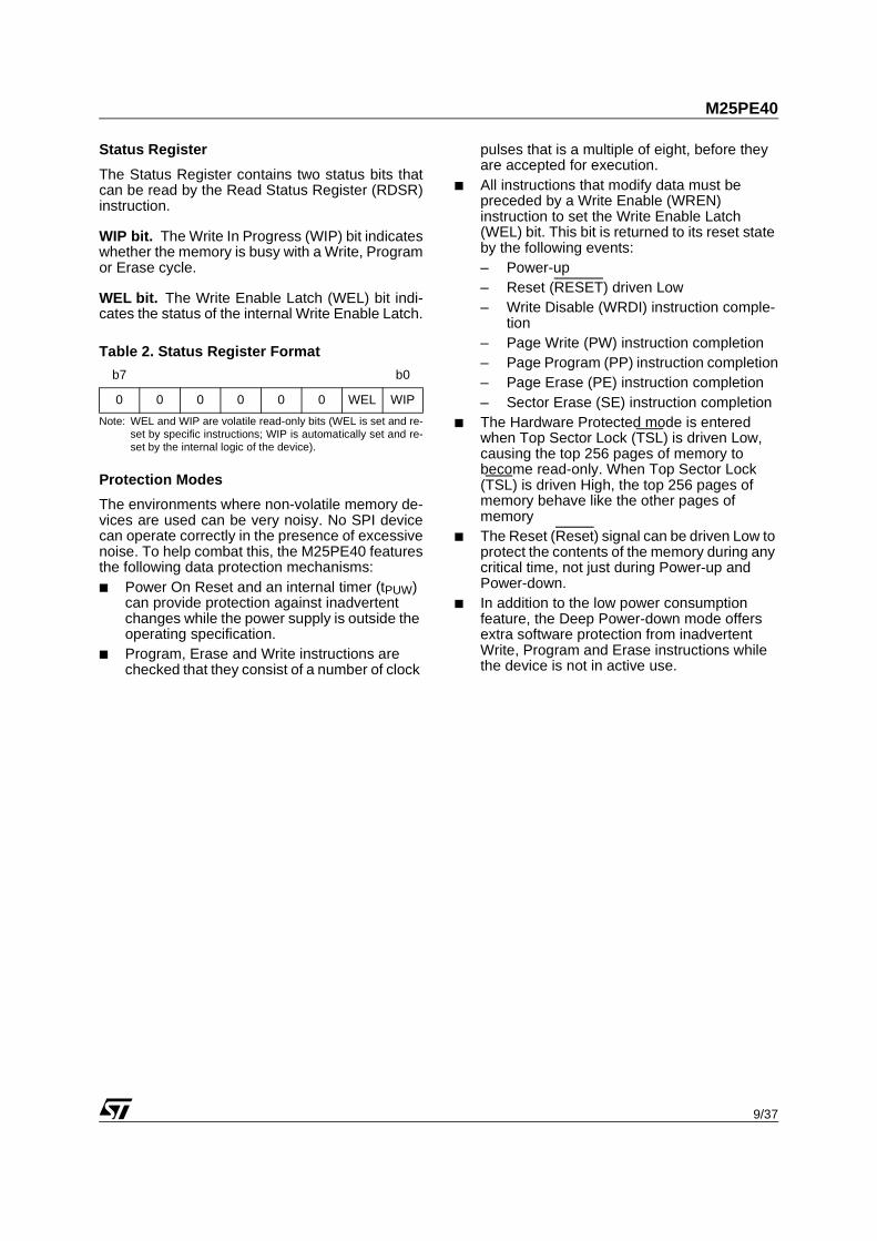
Status Register
The Status Register contains two status bits thatcan be read by the Read Status Register (RDSR)instruction.
WIP bit. The Write In Progress (WIP) bit indicateswhether the memory is busy with a Write, Programor Erase cycle.
WEL bit. The Write Enable Latch (WEL) bit indi-cates the status of the internal Write Enable Latch.
Table 2. Status Register Format
Note: WEL and WIP are volatile read-only bits (WEL is set and re-set by specific instructions; WIP is automatically set and re-set by the internal logic of the device).
Protection Modes
The environments where non-volatile memory de-vices are used can be very noisy. No SPI devicecan operate correctly in the presence of excessivenoise. To help combat this, the M25PE40 featuresthe following data protection mechanisms: Power On Reset and an internal timer (tPUW)
can provide protection against inadvertent changes while the power supply is outside the operating specification.
Program, Erase and Write instructions are checked that they consist of a number of clock
pulses that is a multiple of eight, before they are accepted for execution.
All instructions that modify data must be preceded by a Write Enable (WREN) instruction to set the Write Enable Latch (WEL) bit. This bit is returned to its reset state by the following events:– Power-up– Reset (RESET) driven Low– Write Disable (WRDI) instruction comple-
tion– Page Write (PW) instruction completion– Page Program (PP) instruction completion– Page Erase (PE) instruction completion– Sector Erase (SE) instruction completion
The Hardware Protected mode is entered when Top Sector Lock (TSL) is driven Low, causing the top 256 pages of memory to become read-only. When Top Sector Lock (TSL) is driven High, the top 256 pages of memory behave like the other pages of memory
The Reset (Reset) signal can be driven Low to protect the contents of the memory during any critical time, not just during Power-up and Power-down.
In addition to the low power consumption feature, the Deep Power-down mode offers extra software protection from inadvertent Write, Program and Erase instructions while the device is not in active use.
b7 b0
0 0 0 0 0 0 WEL WIP
M25PE40
10/37
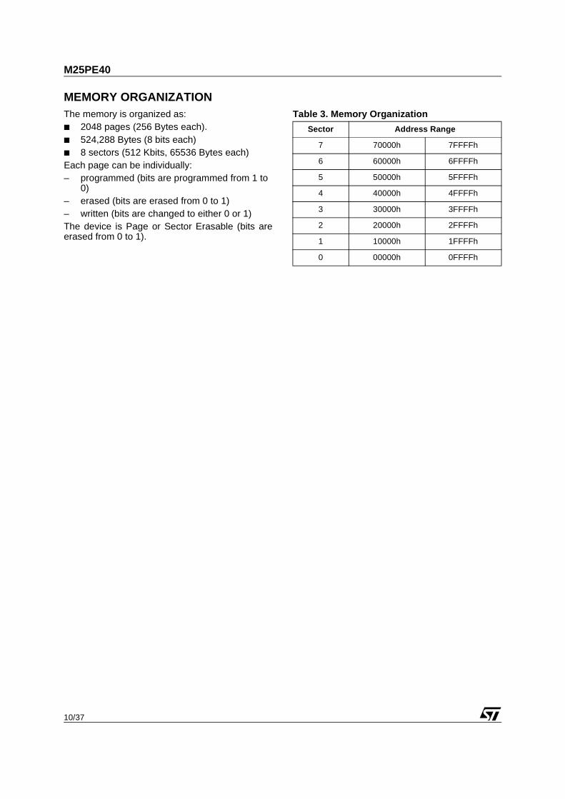
MEMORY ORGANIZATIONThe memory is organized as: 2048 pages (256 Bytes each). 524,288 Bytes (8 bits each) 8 sectors (512 Kbits, 65536 Bytes each)Each page can be individually:– programmed (bits are programmed from 1 to
0)– erased (bits are erased from 0 to 1)– written (bits are changed to either 0 or 1)The device is Page or Sector Erasable (bits areerased from 0 to 1).
Table 3. Memory Organization
Sector Address Range
7 70000h 7FFFFh
6 60000h 6FFFFh
5 50000h 5FFFFh
4 40000h 4FFFFh
3 30000h 3FFFFh
2 20000h 2FFFFh
1 10000h 1FFFFh
0 00000h 0FFFFh
11/37
M25PE40
Figure 6. Block Diagram
AI04042d
S
TSL Control LogicHigh Voltage
Generator
I/O Shift Register
Address Registerand Counter
256 ByteData Buffer
256 Bytes (Page Size)
X Decoder
Y D
ecod
er
C
D
Q
StatusRegister
00000h
7FFFFh
000FFh
Reset
6FFFFh
Top 256 Pages canbe made read-only
M25PE40
12/37
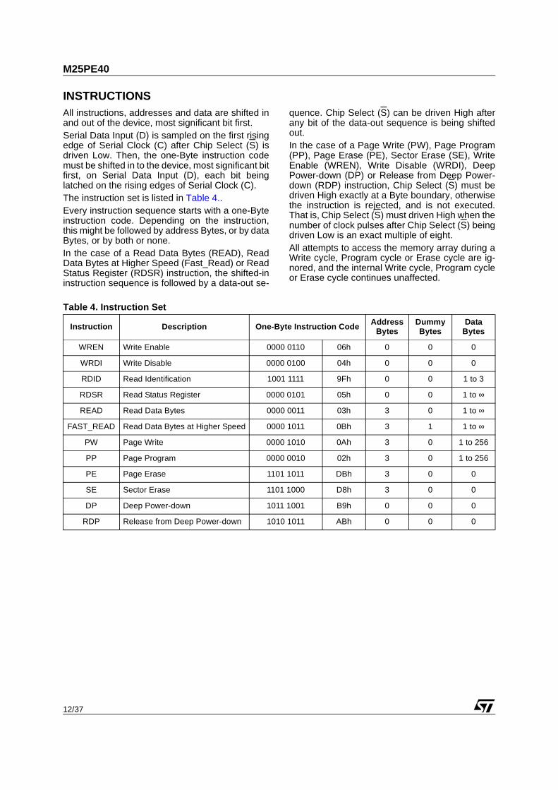
INSTRUCTIONSAll instructions, addresses and data are shifted inand out of the device, most significant bit first.Serial Data Input (D) is sampled on the first risingedge of Serial Clock (C) after Chip Select (S) isdriven Low. Then, the one-Byte instruction codemust be shifted in to the device, most significant bitfirst, on Serial Data Input (D), each bit beinglatched on the rising edges of Serial Clock (C).The instruction set is listed in Table 4.. Every instruction sequence starts with a one-Byteinstruction code. Depending on the instruction,this might be followed by address Bytes, or by dataBytes, or by both or none.In the case of a Read Data Bytes (READ), ReadData Bytes at Higher Speed (Fast_Read) or ReadStatus Register (RDSR) instruction, the shifted-ininstruction sequence is followed by a data-out se-
quence. Chip Select (S) can be driven High afterany bit of the data-out sequence is being shiftedout.In the case of a Page Write (PW), Page Program(PP), Page Erase (PE), Sector Erase (SE), WriteEnable (WREN), Write Disable (WRDI), DeepPower-down (DP) or Release from Deep Power-down (RDP) instruction, Chip Select (S) must bedriven High exactly at a Byte boundary, otherwisethe instruction is rejected, and is not executed.That is, Chip Select (S) must driven High when thenumber of clock pulses after Chip Select (S) beingdriven Low is an exact multiple of eight. All attempts to access the memory array during aWrite cycle, Program cycle or Erase cycle are ig-nored, and the internal Write cycle, Program cycleor Erase cycle continues unaffected.
Table 4. Instruction Set
Instruction Description One-Byte Instruction Code Address Bytes
Dummy Bytes
Data Bytes
WREN Write Enable 0000 0110 06h 0 0 0
WRDI Write Disable 0000 0100 04h 0 0 0
RDID Read Identification 1001 1111 9Fh 0 0 1 to 3
RDSR Read Status Register 0000 0101 05h 0 0 1 to ∞
READ Read Data Bytes 0000 0011 03h 3 0 1 to ∞
FAST_READ Read Data Bytes at Higher Speed 0000 1011 0Bh 3 1 1 to ∞
PW Page Write 0000 1010 0Ah 3 0 1 to 256
PP Page Program 0000 0010 02h 3 0 1 to 256
PE Page Erase 1101 1011 DBh 3 0 0
SE Sector Erase 1101 1000 D8h 3 0 0
DP Deep Power-down 1011 1001 B9h 0 0 0
RDP Release from Deep Power-down 1010 1011 ABh 0 0 0
13/37
M25PE40
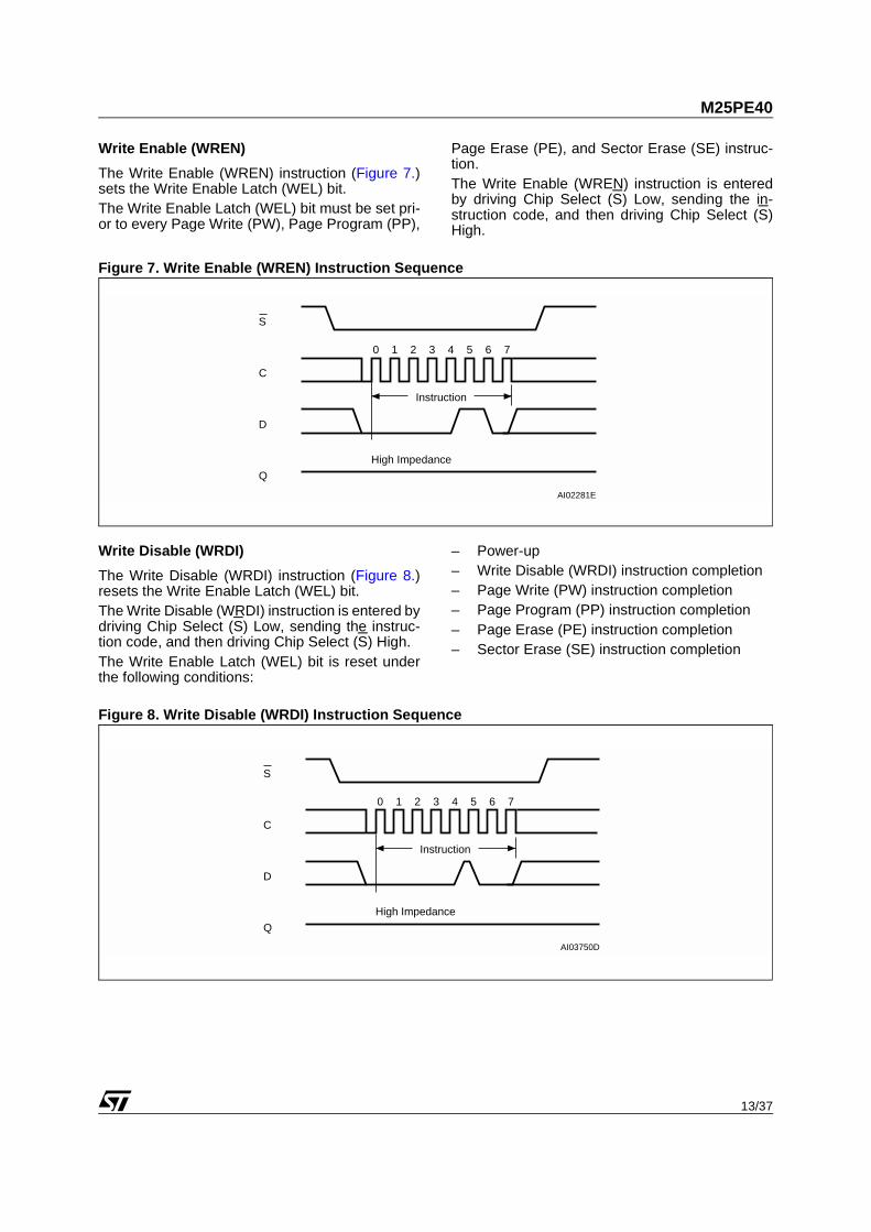
Write Enable (WREN)
The Write Enable (WREN) instruction (Figure 7.)sets the Write Enable Latch (WEL) bit. The Write Enable Latch (WEL) bit must be set pri-or to every Page Write (PW), Page Program (PP),
Page Erase (PE), and Sector Erase (SE) instruc-tion.The Write Enable (WREN) instruction is enteredby driving Chip Select (S) Low, sending the in-struction code, and then driving Chip Select (S)High.
Figure 7. Write Enable (WREN) Instruction Sequence
Write Disable (WRDI)
The Write Disable (WRDI) instruction (Figure 8.)resets the Write Enable Latch (WEL) bit. The Write Disable (WRDI) instruction is entered bydriving Chip Select (S) Low, sending the instruc-tion code, and then driving Chip Select (S) High.The Write Enable Latch (WEL) bit is reset underthe following conditions:
– Power-up– Write Disable (WRDI) instruction completion– Page Write (PW) instruction completion– Page Program (PP) instruction completion– Page Erase (PE) instruction completion– Sector Erase (SE) instruction completion
Figure 8. Write Disable (WRDI) Instruction Sequence
C
D
AI02281E
S
Q
21 3 4 5 6 7
High Impedance
0
Instruction
C
D
AI03750D
S
Q
21 3 4 5 6 7
High Impedance
0
Instruction
M25PE40
14/37
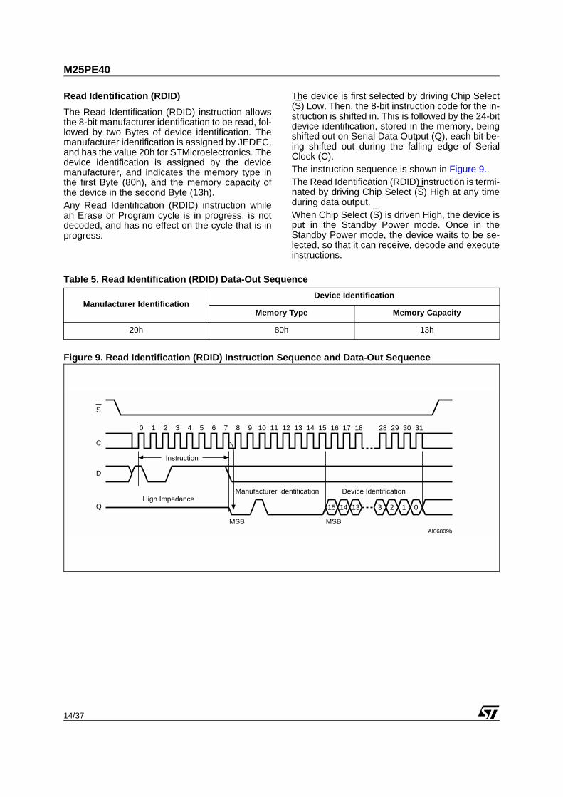
Read Identification (RDID)
The Read Identification (RDID) instruction allowsthe 8-bit manufacturer identification to be read, fol-lowed by two Bytes of device identification. Themanufacturer identification is assigned by JEDEC,and has the value 20h for STMicroelectronics. Thedevice identification is assigned by the devicemanufacturer, and indicates the memory type inthe first Byte (80h), and the memory capacity ofthe device in the second Byte (13h).Any Read Identification (RDID) instruction whilean Erase or Program cycle is in progress, is notdecoded, and has no effect on the cycle that is inprogress.
The device is first selected by driving Chip Select(S) Low. Then, the 8-bit instruction code for the in-struction is shifted in. This is followed by the 24-bitdevice identification, stored in the memory, beingshifted out on Serial Data Output (Q), each bit be-ing shifted out during the falling edge of SerialClock (C).The instruction sequence is shown in Figure 9..The Read Identification (RDID) instruction is termi-nated by driving Chip Select (S) High at any timeduring data output.When Chip Select (S) is driven High, the device isput in the Standby Power mode. Once in theStandby Power mode, the device waits to be se-lected, so that it can receive, decode and executeinstructions.
Table 5. Read Identification (RDID) Data-Out Sequence
Figure 9. Read Identification (RDID) Instruction Sequence and Data-Out Sequence
Manufacturer IdentificationDevice Identification
Memory Type Memory Capacity
20h 80h 13h
C
D
S
21 3 4 5 6 7 8 9 10 11 12 13 14 15
Instruction
0
AI06809b
Q
Manufacturer IdentificationHigh Impedance
MSB
15 14 13 3 2 1 0
Device Identification
MSB
16 17 18 28 29 30 31

15/37
M25PE40
Read Status Register (RDSR)
The Read Status Register (RDSR) instruction al-lows the Status Register to be read. The StatusRegister may be read at any time, even while aProgram, Erase or Write cycle is in progress.When one of these cycles is in progress, it is rec-ommended to check the Write In Progress (WIP)bit before sending a new instruction to the device.It is also possible to read the Status Register con-tinuously, as shown in Figure 10..The status bits of the Status Register are as fol-lows:
WIP bit. The Write In Progress (WIP) bit indicateswhether the memory is busy with a Write, Programor Erase cycle. When set to 1, such a cycle is inprogress, when reset to 0 no such cycle is inprogress.
WEL bit. The Write Enable Latch (WEL) bit indi-cates the status of the internal Write Enable Latch.When set to 1 the internal Write Enable Latch isset, when set to 0 the internal Write Enable Latchis reset and no Write, Program or Erase instructionis accepted.
Figure 10. Read Status Register (RDSR) Instruction Sequence and Data-Out Sequence
C
D
S
21 3 4 5 6 7 8 9 10 11 12 13 14 15
Instruction
0
AI02031E
Q 7 6 5 4 3 2 1 0
Status Register OutHigh Impedance
MSB
7 6 5 4 3 2 1 0
Status Register Out
MSB
7
M25PE40
16/37
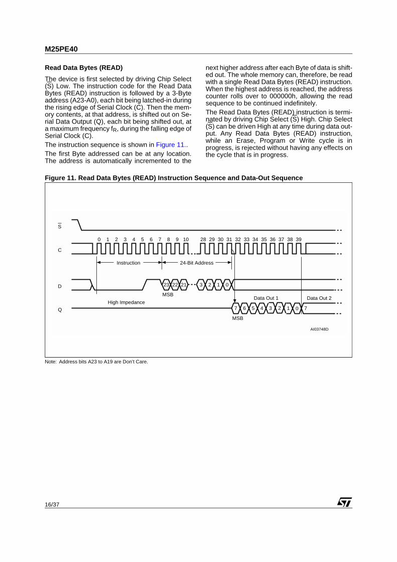
Read Data Bytes (READ)
The device is first selected by driving Chip Select(S) Low. The instruction code for the Read DataBytes (READ) instruction is followed by a 3-Byteaddress (A23-A0), each bit being latched-in duringthe rising edge of Serial Clock (C). Then the mem-ory contents, at that address, is shifted out on Se-rial Data Output (Q), each bit being shifted out, ata maximum frequency fR, during the falling edge ofSerial Clock (C).The instruction sequence is shown in Figure 11..The first Byte addressed can be at any location.The address is automatically incremented to the
next higher address after each Byte of data is shift-ed out. The whole memory can, therefore, be readwith a single Read Data Bytes (READ) instruction.When the highest address is reached, the addresscounter rolls over to 000000h, allowing the readsequence to be continued indefinitely.The Read Data Bytes (READ) instruction is termi-nated by driving Chip Select (S) High. Chip Select(S) can be driven High at any time during data out-put. Any Read Data Bytes (READ) instruction,while an Erase, Program or Write cycle is inprogress, is rejected without having any effects onthe cycle that is in progress.
Figure 11. Read Data Bytes (READ) Instruction Sequence and Data-Out Sequence
Note: Address bits A23 to A19 are Don’t Care.
C
D
AI03748D
S
Q
23
21 3 4 5 6 7 8 9 10 28 29 30 31 32 33 34 35
22 21 3 2 1 0
36 37 38
7 6 5 4 3 1 70High Impedance
Data Out 1
Instruction 24-Bit Address
0
MSB
MSB
2
39
Data Out 2
17/37
M25PE40
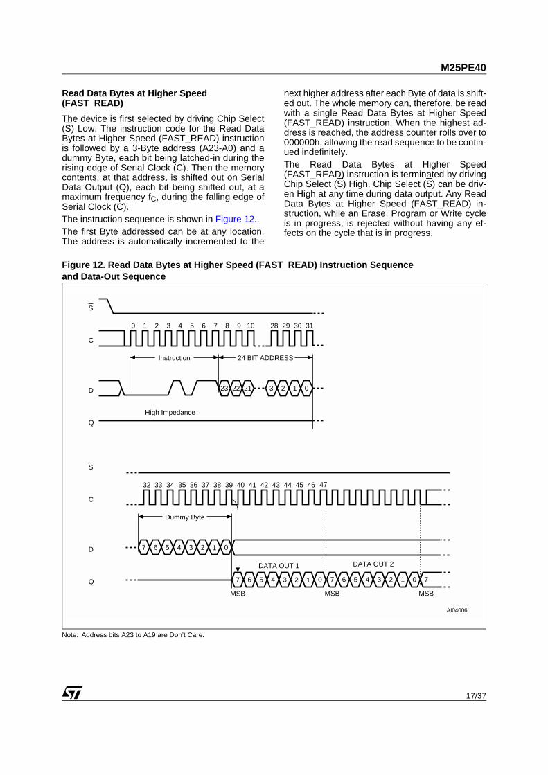
Read Data Bytes at Higher Speed (FAST_READ)
The device is first selected by driving Chip Select(S) Low. The instruction code for the Read DataBytes at Higher Speed (FAST_READ) instructionis followed by a 3-Byte address (A23-A0) and adummy Byte, each bit being latched-in during therising edge of Serial Clock (C). Then the memorycontents, at that address, is shifted out on SerialData Output (Q), each bit being shifted out, at amaximum frequency fC, during the falling edge ofSerial Clock (C).The instruction sequence is shown in Figure 12..The first Byte addressed can be at any location.The address is automatically incremented to the
next higher address after each Byte of data is shift-ed out. The whole memory can, therefore, be readwith a single Read Data Bytes at Higher Speed(FAST_READ) instruction. When the highest ad-dress is reached, the address counter rolls over to000000h, allowing the read sequence to be contin-ued indefinitely.The Read Data Bytes at Higher Speed(FAST_READ) instruction is terminated by drivingChip Select (S) High. Chip Select (S) can be driv-en High at any time during data output. Any ReadData Bytes at Higher Speed (FAST_READ) in-struction, while an Erase, Program or Write cycleis in progress, is rejected without having any ef-fects on the cycle that is in progress.
Figure 12. Read Data Bytes at Higher Speed (FAST_READ) Instruction Sequenceand Data-Out Sequence
Note: Address bits A23 to A19 are Don’t Care.
C
D
AI04006
S
Q
23
21 3 4 5 6 7 8 9 10 28 29 30 31
22 21 3 2 1 0
High Impedance
Instruction 24 BIT ADDRESS
0
C
D
S
Q
32 33 34 36 37 38 39 40 41 42 43 44 45 46
7 6 5 4 3 2 01
DATA OUT 1
Dummy Byte
MSB
7 6 5 4 3 2 1 0
DATA OUT 2
MSB MSB
7
47
7 6 5 4 3 2 01
35
M25PE40
18/37
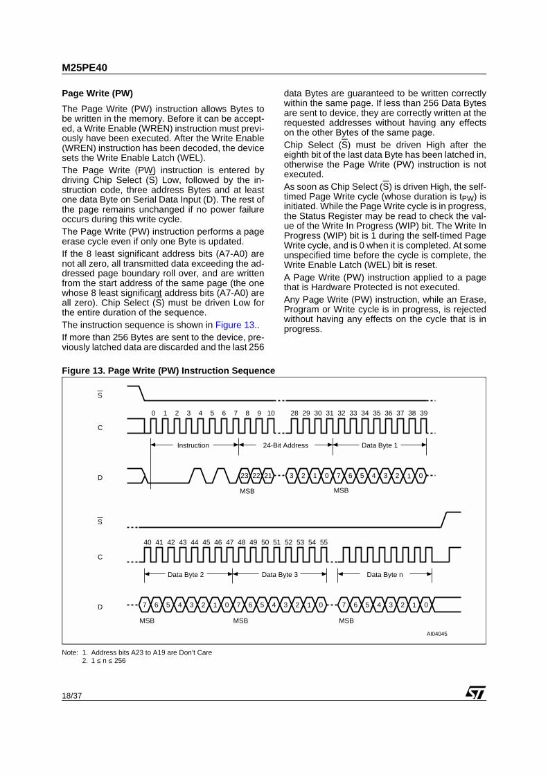
Page Write (PW)
The Page Write (PW) instruction allows Bytes tobe written in the memory. Before it can be accept-ed, a Write Enable (WREN) instruction must previ-ously have been executed. After the Write Enable(WREN) instruction has been decoded, the devicesets the Write Enable Latch (WEL).The Page Write (PW) instruction is entered bydriving Chip Select (S) Low, followed by the in-struction code, three address Bytes and at leastone data Byte on Serial Data Input (D). The rest ofthe page remains unchanged if no power failureoccurs during this write cycle.The Page Write (PW) instruction performs a pageerase cycle even if only one Byte is updated.If the 8 least significant address bits (A7-A0) arenot all zero, all transmitted data exceeding the ad-dressed page boundary roll over, and are writtenfrom the start address of the same page (the onewhose 8 least significant address bits (A7-A0) areall zero). Chip Select (S) must be driven Low forthe entire duration of the sequence.The instruction sequence is shown in Figure 13..If more than 256 Bytes are sent to the device, pre-viously latched data are discarded and the last 256
data Bytes are guaranteed to be written correctlywithin the same page. If less than 256 Data Bytesare sent to device, they are correctly written at therequested addresses without having any effectson the other Bytes of the same page. Chip Select (S) must be driven High after theeighth bit of the last data Byte has been latched in,otherwise the Page Write (PW) instruction is notexecuted.As soon as Chip Select (S) is driven High, the self-timed Page Write cycle (whose duration is tPW) isinitiated. While the Page Write cycle is in progress,the Status Register may be read to check the val-ue of the Write In Progress (WIP) bit. The Write InProgress (WIP) bit is 1 during the self-timed PageWrite cycle, and is 0 when it is completed. At someunspecified time before the cycle is complete, theWrite Enable Latch (WEL) bit is reset.A Page Write (PW) instruction applied to a pagethat is Hardware Protected is not executed.Any Page Write (PW) instruction, while an Erase,Program or Write cycle is in progress, is rejectedwithout having any effects on the cycle that is inprogress.
Figure 13. Page Write (PW) Instruction Sequence
Note: 1. Address bits A23 to A19 are Don’t Care2. 1 ≤ n ≤ 256
C
D
AI04045
S
4241 43 44 45 46 47 48 49 50 52 53 54 5540
C
D
S
23
21 3 4 5 6 7 8 9 10 28 29 30 31 32 33 34 35
22 21 3 2 1 0
36 37 38
Instruction 24-Bit Address
0
7 6 5 4 3 2 01
Data Byte 1
39
51
7 6 5 4 3 2 01
Data Byte 2
7 6 5 4 3 2 01
Data Byte 3 Data Byte n
7 6 5 4 3 2 01
MSB MSB
MSB MSB MSB
19/37
M25PE40
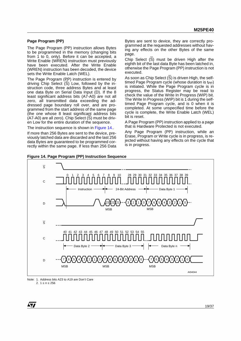
Page Program (PP)
The Page Program (PP) instruction allows Bytesto be programmed in the memory (changing bitsfrom 1 to 0, only). Before it can be accepted, aWrite Enable (WREN) instruction must previouslyhave been executed. After the Write Enable(WREN) instruction has been decoded, the devicesets the Write Enable Latch (WEL).The Page Program (PP) instruction is entered bydriving Chip Select (S) Low, followed by the in-struction code, three address Bytes and at leastone data Byte on Serial Data Input (D). If the 8least significant address bits (A7-A0) are not allzero, all transmitted data exceeding the ad-dressed page boundary roll over, and are pro-grammed from the start address of the same page(the one whose 8 least significant address bits(A7-A0) are all zero). Chip Select (S) must be driv-en Low for the entire duration of the sequence.The instruction sequence is shown in Figure 14..If more than 256 Bytes are sent to the device, pre-viously latched data are discarded and the last 256data Bytes are guaranteed to be programmed cor-rectly within the same page. If less than 256 Data
Bytes are sent to device, they are correctly pro-grammed at the requested addresses without hav-ing any effects on the other Bytes of the samepage. Chip Select (S) must be driven High after theeighth bit of the last data Byte has been latched in,otherwise the Page Program (PP) instruction is notexecuted.As soon as Chip Select (S) is driven High, the self-timed Page Program cycle (whose duration is tPP)is initiated. While the Page Program cycle is inprogress, the Status Register may be read tocheck the value of the Write In Progress (WIP) bit.The Write In Progress (WIP) bit is 1 during the self-timed Page Program cycle, and is 0 when it iscompleted. At some unspecified time before thecycle is complete, the Write Enable Latch (WEL)bit is reset.A Page Program (PP) instruction applied to a pagethat is Hardware Protected is not executed.Any Page Program (PP) instruction, while anErase, Program or Write cycle is in progress, is re-jected without having any effects on the cycle thatis in progress.
Figure 14. Page Program (PP) Instruction Sequence
Note: 1. Address bits A23 to A19 are Don’t Care2. 1 ≤ n ≤ 256
C
D
AI04044
S
4241 43 44 45 46 47 48 49 50 52 53 54 5540
C
D
S
23
21 3 4 5 6 7 8 9 10 28 29 30 31 32 33 34 35
22 21 3 2 1 0
36 37 38
Instruction 24-Bit Address
0
7 6 5 4 3 2 01
Data Byte 1
39
51
7 6 5 4 3 2 01
Data Byte 2
7 6 5 4 3 2 01
Data Byte 3 Data Byte n
7 6 5 4 3 2 01
MSB MSB
MSB MSB MSB
M25PE40
20/37
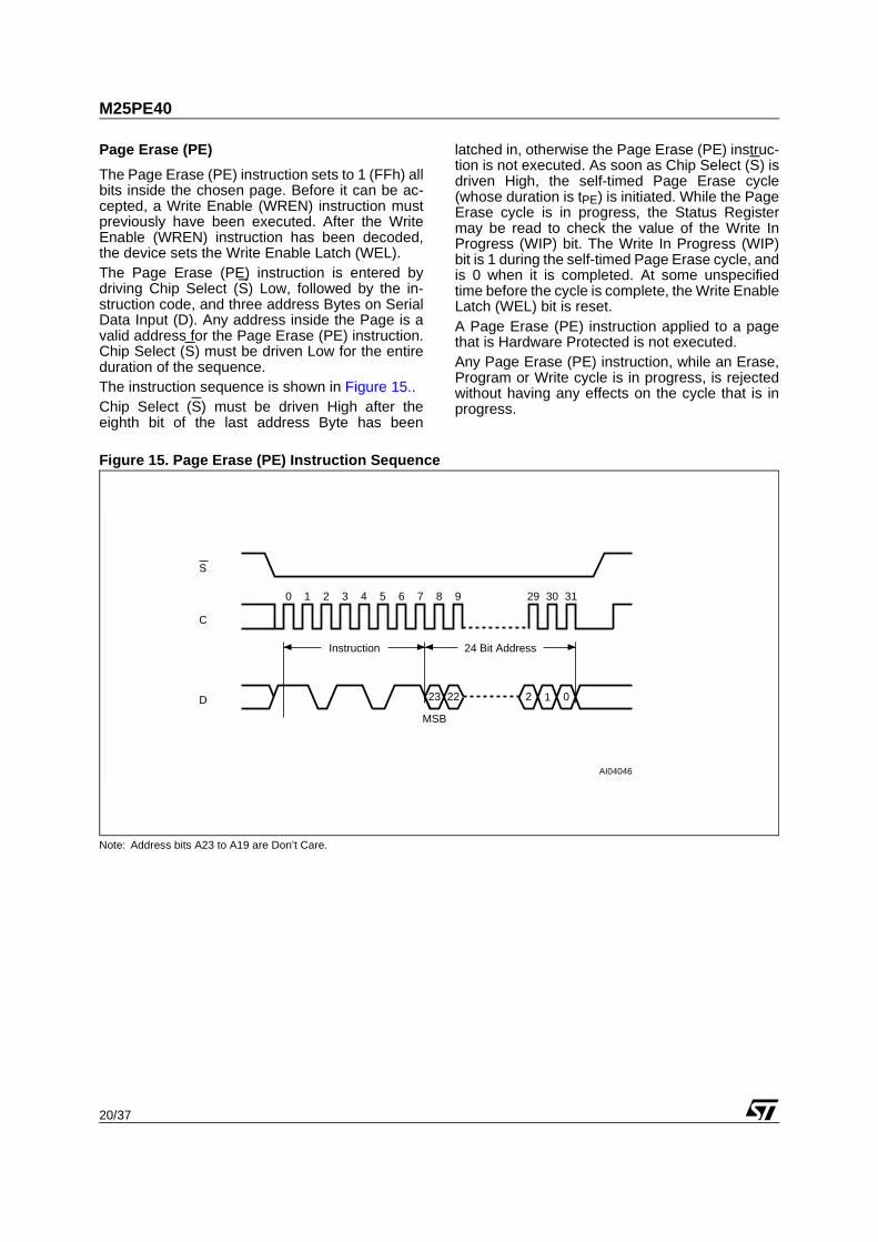
Page Erase (PE)
The Page Erase (PE) instruction sets to 1 (FFh) allbits inside the chosen page. Before it can be ac-cepted, a Write Enable (WREN) instruction mustpreviously have been executed. After the WriteEnable (WREN) instruction has been decoded,the device sets the Write Enable Latch (WEL).The Page Erase (PE) instruction is entered bydriving Chip Select (S) Low, followed by the in-struction code, and three address Bytes on SerialData Input (D). Any address inside the Page is avalid address for the Page Erase (PE) instruction.Chip Select (S) must be driven Low for the entireduration of the sequence. The instruction sequence is shown in Figure 15..Chip Select (S) must be driven High after theeighth bit of the last address Byte has been
latched in, otherwise the Page Erase (PE) instruc-tion is not executed. As soon as Chip Select (S) isdriven High, the self-timed Page Erase cycle(whose duration is tPE) is initiated. While the PageErase cycle is in progress, the Status Registermay be read to check the value of the Write InProgress (WIP) bit. The Write In Progress (WIP)bit is 1 during the self-timed Page Erase cycle, andis 0 when it is completed. At some unspecifiedtime before the cycle is complete, the Write EnableLatch (WEL) bit is reset.A Page Erase (PE) instruction applied to a pagethat is Hardware Protected is not executed.Any Page Erase (PE) instruction, while an Erase,Program or Write cycle is in progress, is rejectedwithout having any effects on the cycle that is inprogress.
Figure 15. Page Erase (PE) Instruction Sequence
Note: Address bits A23 to A19 are Don’t Care.
24 Bit Address
C
D
AI04046
S
21 3 4 5 6 7 8 9 29 30 31
Instruction
0
23 22 2 01
MSB
21/37
M25PE40
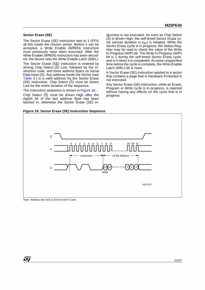
Sector Erase (SE)
The Sector Erase (SE) instruction sets to 1 (FFh)all bits inside the chosen sector. Before it can beaccepted, a Write Enable (WREN) instructionmust previously have been executed. After theWrite Enable (WREN) instruction has been decod-ed, the device sets the Write Enable Latch (WEL).The Sector Erase (SE) instruction is entered bydriving Chip Select (S) Low, followed by the in-struction code, and three address Bytes on SerialData Input (D). Any address inside the Sector (seeTable 3.) is a valid address for the Sector Erase(SE) instruction. Chip Select (S) must be drivenLow for the entire duration of the sequence. The instruction sequence is shown in Figure 16..Chip Select (S) must be driven High after theeighth bit of the last address Byte has beenlatched in, otherwise the Sector Erase (SE) in-
struction is not executed. As soon as Chip Select(S) is driven High, the self-timed Sector Erase cy-cle (whose duration is tSE) is initiated. While theSector Erase cycle is in progress, the Status Reg-ister may be read to check the value of the WriteIn Progress (WIP) bit. The Write In Progress (WIP)bit is 1 during the self-timed Sector Erase cycle,and is 0 when it is completed. At some unspecifiedtime before the cycle is complete, the Write EnableLatch (WEL) bit is reset.A Sector Erase (SE) instruction applied to a sectorthat contains a page that is Hardware Protected isnot executed.Any Sector Erase (SE) instruction, while an Erase,Program or Write cycle is in progress, is rejectedwithout having any effects on the cycle that is inprogress.
Figure 16. Sector Erase (SE) Instruction Sequence
Note: Address bits A23 to A19 are Don’t Care.
24 Bit Address
C
D
AI03751D
S
21 3 4 5 6 7 8 9 29 30 31
Instruction
0
23 22 2 01
MSB
M25PE40
22/37
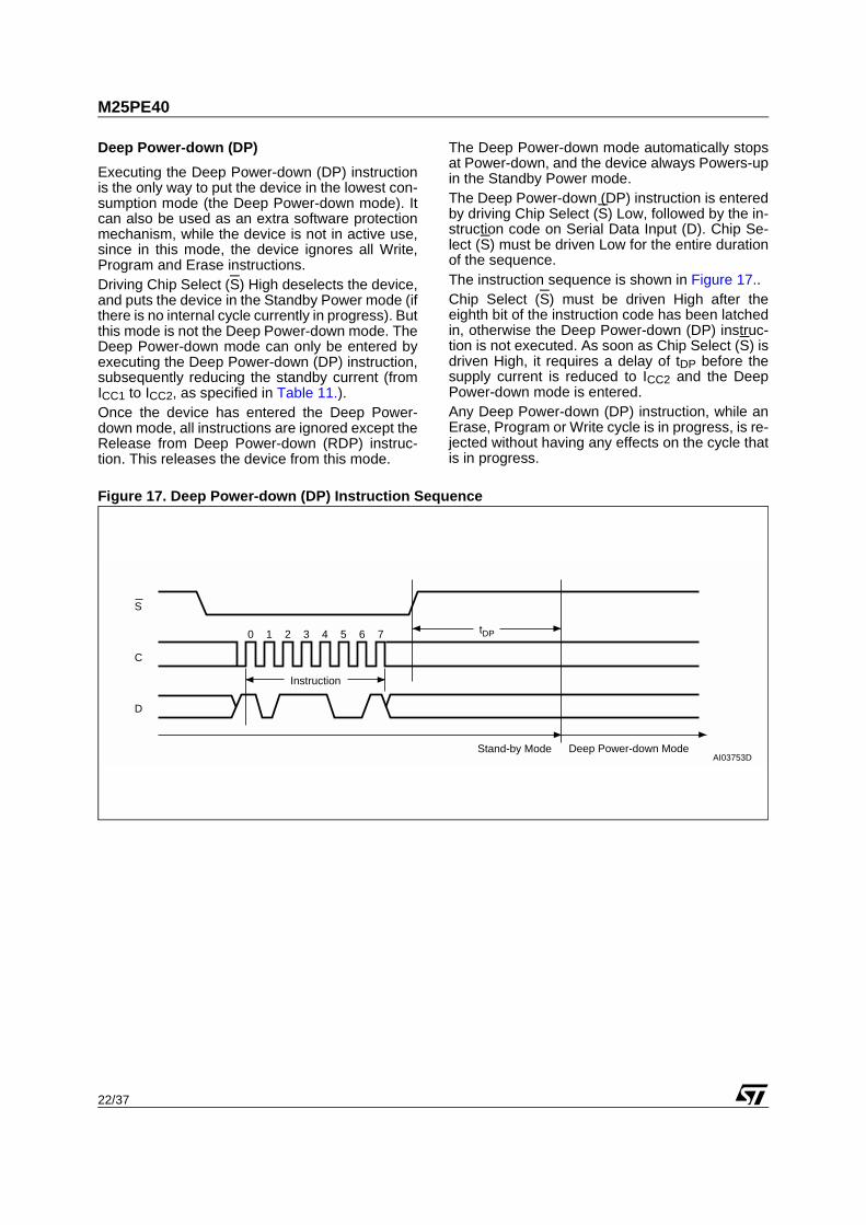
Deep Power-down (DP)
Executing the Deep Power-down (DP) instructionis the only way to put the device in the lowest con-sumption mode (the Deep Power-down mode). Itcan also be used as an extra software protectionmechanism, while the device is not in active use,since in this mode, the device ignores all Write,Program and Erase instructions.Driving Chip Select (S) High deselects the device,and puts the device in the Standby Power mode (ifthere is no internal cycle currently in progress). Butthis mode is not the Deep Power-down mode. TheDeep Power-down mode can only be entered byexecuting the Deep Power-down (DP) instruction,subsequently reducing the standby current (fromICC1 to ICC2, as specified in Table 11.).Once the device has entered the Deep Power-down mode, all instructions are ignored except theRelease from Deep Power-down (RDP) instruc-tion. This releases the device from this mode.
The Deep Power-down mode automatically stopsat Power-down, and the device always Powers-upin the Standby Power mode.The Deep Power-down (DP) instruction is enteredby driving Chip Select (S) Low, followed by the in-struction code on Serial Data Input (D). Chip Se-lect (S) must be driven Low for the entire durationof the sequence.The instruction sequence is shown in Figure 17..Chip Select (S) must be driven High after theeighth bit of the instruction code has been latchedin, otherwise the Deep Power-down (DP) instruc-tion is not executed. As soon as Chip Select (S) isdriven High, it requires a delay of tDP before thesupply current is reduced to ICC2 and the DeepPower-down mode is entered.Any Deep Power-down (DP) instruction, while anErase, Program or Write cycle is in progress, is re-jected without having any effects on the cycle thatis in progress.
Figure 17. Deep Power-down (DP) Instruction Sequence
C
D
AI03753D
S
21 3 4 5 6 70 tDP
Deep Power-down ModeStand-by Mode
Instruction
23/37
M25PE40
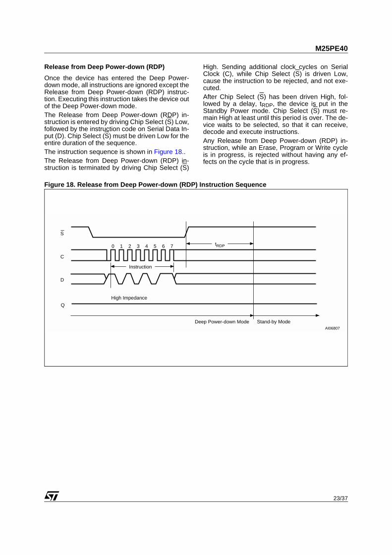
Release from Deep Power-down (RDP)
Once the device has entered the Deep Power-down mode, all instructions are ignored except theRelease from Deep Power-down (RDP) instruc-tion. Executing this instruction takes the device outof the Deep Power-down mode.The Release from Deep Power-down (RDP) in-struction is entered by driving Chip Select (S) Low,followed by the instruction code on Serial Data In-put (D). Chip Select (S) must be driven Low for theentire duration of the sequence.The instruction sequence is shown in Figure 18..The Release from Deep Power-down (RDP) in-struction is terminated by driving Chip Select (S)
High. Sending additional clock cycles on SerialClock (C), while Chip Select (S) is driven Low,cause the instruction to be rejected, and not exe-cuted.After Chip Select (S) has been driven High, fol-lowed by a delay, tRDP, the device is put in theStandby Power mode. Chip Select (S) must re-main High at least until this period is over. The de-vice waits to be selected, so that it can receive,decode and execute instructions.Any Release from Deep Power-down (RDP) in-struction, while an Erase, Program or Write cycleis in progress, is rejected without having any ef-fects on the cycle that is in progress.
Figure 18. Release from Deep Power-down (RDP) Instruction Sequence
C
D
AI06807
S
21 3 4 5 6 70 tRDP
Stand-by ModeDeep Power-down Mode
Q
High Impedance
Instruction
M25PE40
24/37
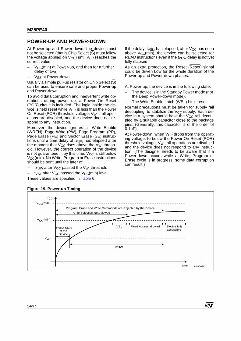
POWER-UP AND POWER-DOWNAt Power-up and Power-down, the device mustnot be selected (that is Chip Select (S) must followthe voltage applied on VCC) until VCC reaches thecorrect value: – VCC(min) at Power-up, and then for a further
delay of tVSL
– VSS at Power-downUsually a simple pull-up resistor on Chip Select (S)can be used to ensure safe and proper Power-upand Power-down.To avoid data corruption and inadvertent write op-erations during power up, a Power On Reset(POR) circuit is included. The logic inside the de-vice is held reset while VCC is less than the PowerOn Reset (POR) threshold voltage, VWI – all oper-ations are disabled, and the device does not re-spond to any instruction.Moreover, the device ignores all Write Enable(WREN), Page Write (PW), Page Program (PP),Page Erase (PE) and Sector Erase (SE) instruc-tions until a time delay of tPUW has elapsed afterthe moment that VCC rises above the VWI thresh-old. However, the correct operation of the deviceis not guaranteed if, by this time, VCC is still belowVCC(min). No Write, Program or Erase instructionsshould be sent until the later of:– tPUW after VCC passed the VWI threshold– tVSL after VCC passed the VCC(min) levelThese values are specified in Table 6.
If the delay, tVSL, has elapsed, after VCC has risenabove VCC(min), the device can be selected forREAD instructions even if the tPUW delay is not yetfully elapsed.As an extra protection, the Reset (Reset) signalcould be driven Low for the whole duration of thePower-up and Power-down phases.
At Power-up, the device is in the following state: – The device is in the Standby Power mode (not
the Deep Power-down mode). – The Write Enable Latch (WEL) bit is reset.Normal precautions must be taken for supply raildecoupling, to stabilize the VCC supply. Each de-vice in a system should have the VCC rail decou-pled by a suitable capacitor close to the packagepins. (Generally, this capacitor is of the order of0.1µF).At Power-down, when VCC drops from the operat-ing voltage, to below the Power On Reset (POR)threshold voltage, VWI, all operations are disabledand the device does not respond to any instruc-tion. (The designer needs to be aware that if aPower-down occurs while a Write, Program orErase cycle is in progress, some data corruptioncan result.)
Figure 19. Power-up Timing
VCC
AI04009C
VCC(min)
VWI
Reset Stateof theDevice
Chip Selection Not Allowed
Program, Erase and Write Commands are Rejected by the Device
tVSL
tPUW
time
Read Access allowed Device fullyaccessible
VCC(max)
25/37
M25PE40
Table 6. Power-Up Timing and VWI Threshold
Note: 1. These parameters are characterized only, over the temperature range –40°C to +85°C.
INITIAL DELIVERY STATEThe device is delivered with the memory arrayerased: all bits are set to 1 (each Byte containsFFh). All usable Status Register bits are 0.
Symbol Parameter Min. Max. Unit
tVSL1 VCC(min) to S low 30 µs
tPUW1 Time delay before the first Write, Program or Erase instruction 1 10 ms
VWI1 Write Inhibit Voltage 1.5 2.5 V
M25PE40
26/37
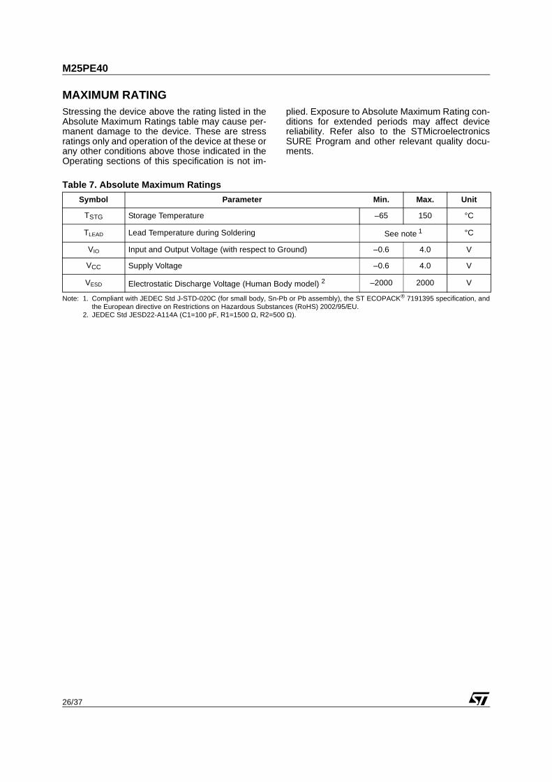
MAXIMUM RATINGStressing the device above the rating listed in theAbsolute Maximum Ratings table may cause per-manent damage to the device. These are stressratings only and operation of the device at these orany other conditions above those indicated in theOperating sections of this specification is not im-
plied. Exposure to Absolute Maximum Rating con-ditions for extended periods may affect devicereliability. Refer also to the STMicroelectronicsSURE Program and other relevant quality docu-ments.
Table 7. Absolute Maximum Ratings
Note: 1. Compliant with JEDEC Std J-STD-020C (for small body, Sn-Pb or Pb assembly), the ST ECOPACK® 7191395 specification, andthe European directive on Restrictions on Hazardous Substances (RoHS) 2002/95/EU.
2. JEDEC Std JESD22-A114A (C1=100 pF, R1=1500 Ω, R2=500 Ω).
Symbol Parameter Min. Max. Unit
TSTG Storage Temperature –65 150 °C
TLEAD Lead Temperature during Soldering See note 1 °C
VIO Input and Output Voltage (with respect to Ground) –0.6 4.0 V
VCC Supply Voltage –0.6 4.0 V
VESD Electrostatic Discharge Voltage (Human Body model) 2 –2000 2000 V
27/37
M25PE40
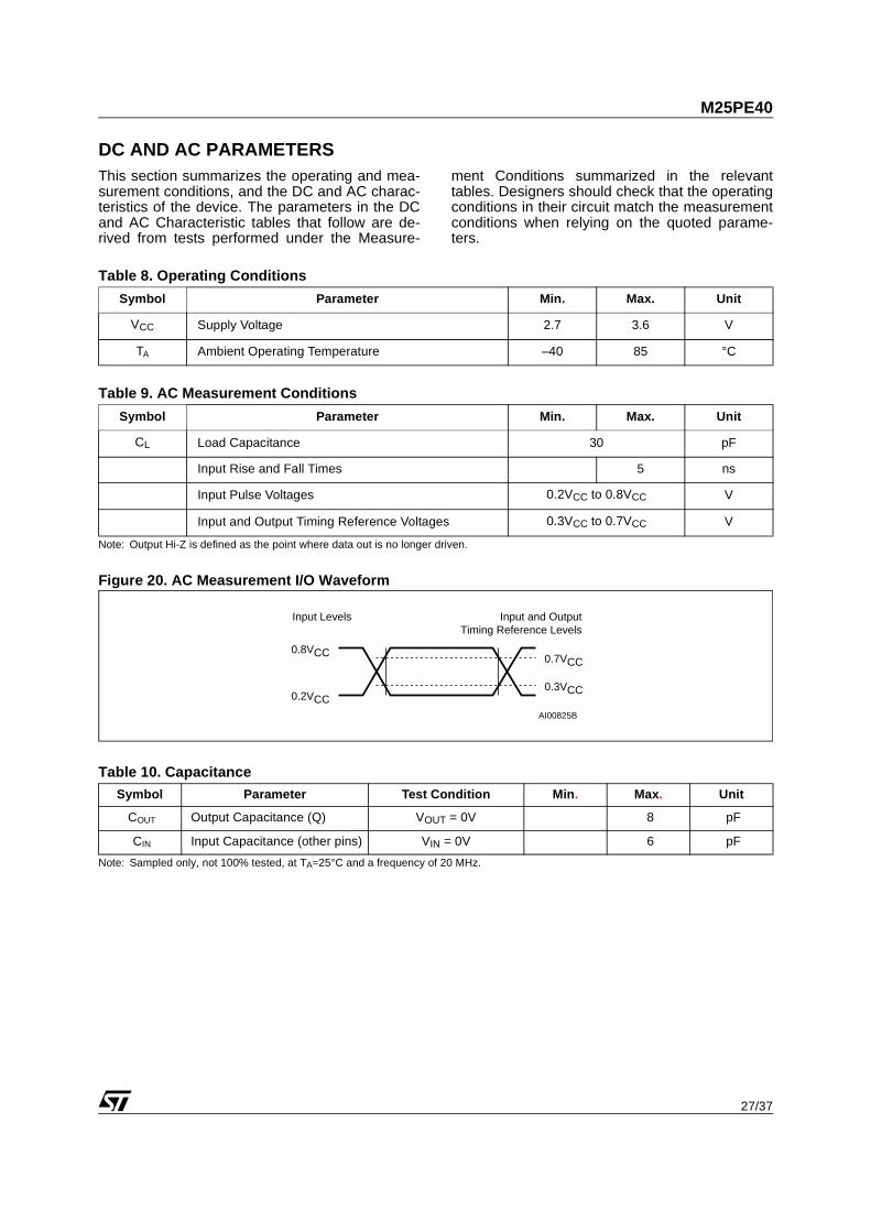
DC AND AC PARAMETERSThis section summarizes the operating and mea-surement conditions, and the DC and AC charac-teristics of the device. The parameters in the DCand AC Characteristic tables that follow are de-rived from tests performed under the Measure-
ment Conditions summarized in the relevanttables. Designers should check that the operatingconditions in their circuit match the measurementconditions when relying on the quoted parame-ters.
Table 8. Operating Conditions
Table 9. AC Measurement Conditions
Note: Output Hi-Z is defined as the point where data out is no longer driven.
Figure 20. AC Measurement I/O Waveform
Table 10. Capacitance
Note: Sampled only, not 100% tested, at TA=25°C and a frequency of 20 MHz.
Symbol Parameter Min. Max. Unit
VCC Supply Voltage 2.7 3.6 V
TA Ambient Operating Temperature –40 85 °C
Symbol Parameter Min. Max. Unit
CL Load Capacitance 30 pF
Input Rise and Fall Times 5 ns
Input Pulse Voltages 0.2VCC to 0.8VCC V
Input and Output Timing Reference Voltages 0.3VCC to 0.7VCC V
Symbol Parameter Test Condition Min. Max. Unit
COUT Output Capacitance (Q) VOUT = 0V 8 pF
CIN Input Capacitance (other pins) VIN = 0V 6 pF
AI00825B
0.8VCC
0.2VCC
0.7VCC
0.3VCC
Input and OutputTiming Reference Levels
Input Levels
M25PE40
28/37
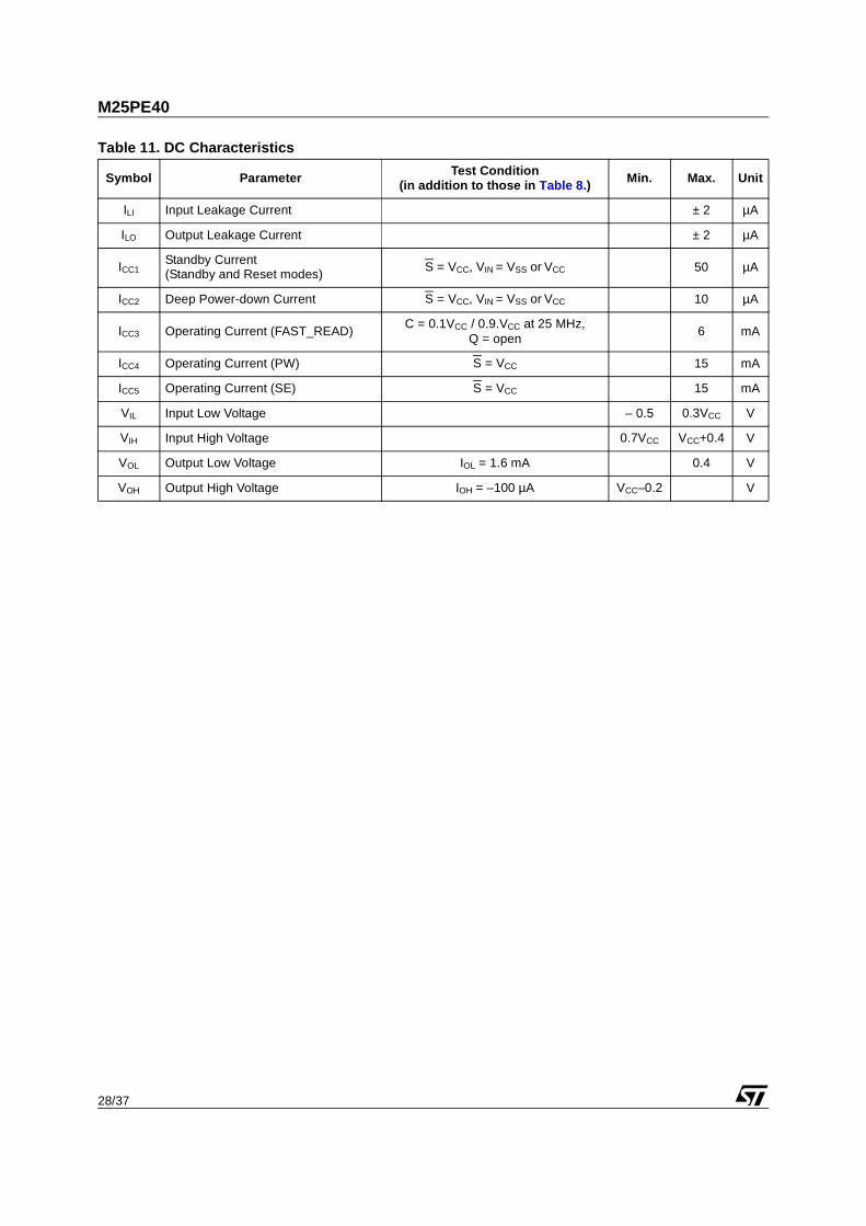
Table 11. DC Characteristics
Symbol Parameter Test Condition(in addition to those in Table 8.) Min. Max. Unit
ILI Input Leakage Current ± 2 µA
ILO Output Leakage Current ± 2 µA
ICC1Standby Current(Standby and Reset modes)
S = VCC, VIN = VSS or VCC 50 µA
ICC2 Deep Power-down Current S = VCC, VIN = VSS or VCC 10 µA
ICC3 Operating Current (FAST_READ)C = 0.1VCC / 0.9.VCC at 25 MHz,
Q = open6 mA
ICC4 Operating Current (PW) S = VCC 15 mA
ICC5 Operating Current (SE) S = VCC 15 mA
VIL Input Low Voltage – 0.5 0.3VCC V
VIH Input High Voltage 0.7VCC VCC+0.4 V
VOL Output Low Voltage IOL = 1.6 mA 0.4 V
VOH Output High Voltage IOH = –100 µA VCC–0.2 V
29/37
M25PE40
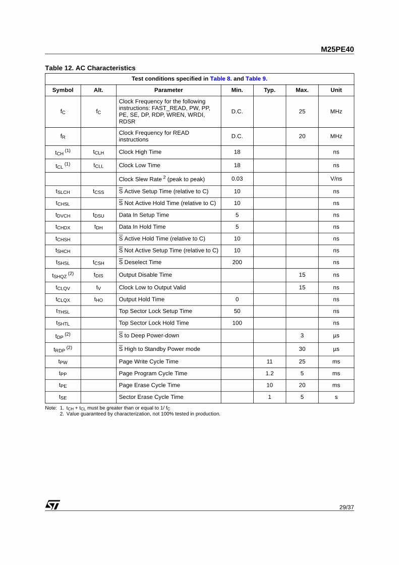
Table 12. AC Characteristics
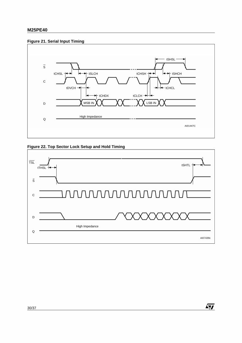
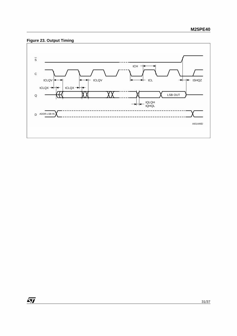
Note: 1. tCH + tCL must be greater than or equal to 1/ fC2. Value guaranteed by characterization, not 100% tested in production.
Test conditions specified in Table 8. and Table 9.
Symbol Alt. Parameter Min. Typ. Max. Unit
fC fC
Clock Frequency for the following instructions: FAST_READ, PW, PP, PE, SE, DP, RDP, WREN, WRDI, RDSR
D.C. 25 MHz
fRClock Frequency for READ instructions
D.C. 20 MHz
tCH (1) tCLH Clock High Time 18 ns
tCL (1) tCLL Clock Low Time 18 ns
Clock Slew Rate 2 (peak to peak) 0.03 V/ns
tSLCH tCSS S Active Setup Time (relative to C) 10 ns
tCHSL S Not Active Hold Time (relative to C) 10 ns
tDVCH tDSU Data In Setup Time 5 ns
tCHDX tDH Data In Hold Time 5 ns
tCHSH S Active Hold Time (relative to C) 10 ns
tSHCH S Not Active Setup Time (relative to C) 10 ns
tSHSL tCSH S Deselect Time 200 ns
tSHQZ (2) tDIS Output Disable Time 15 ns
tCLQV tV Clock Low to Output Valid 15 ns
tCLQX tHO Output Hold Time 0 ns
tTHSL Top Sector Lock Setup Time 50 ns
tSHTL Top Sector Lock Hold Time 100 ns
tDP (2) S to Deep Power-down 3 µs
tRDP (2) S High to Standby Power mode 30 µs
tPW Page Write Cycle Time 11 25 ms
tPP Page Program Cycle Time 1.2 5 ms
tPE Page Erase Cycle Time 10 20 ms
tSE Sector Erase Cycle Time 1 5 s
M25PE40
30/37
Figure 21. Serial Input Timing
Figure 22. Top Sector Lock Setup and Hold Timing
C
D
AI01447C
S
MSB IN
Q
tDVCH
High Impedance
LSB IN
tSLCH
tCHDX
tCHCL
tCLCH
tSHCH
tSHSL
tCHSHtCHSL
C
D
S
Q
High Impedance
TSL
tTHSLtSHTL
AI07439c
31/37
M25PE40
Figure 23. Output Timing
C
Q
AI01449D
S
LSB OUT
D ADDR.LSB IN
tSHQZ
tCH
tCL
tQLQHtQHQL
tCLQX
tCLQV
tCLQX
tCLQV
M25PE40
32/37
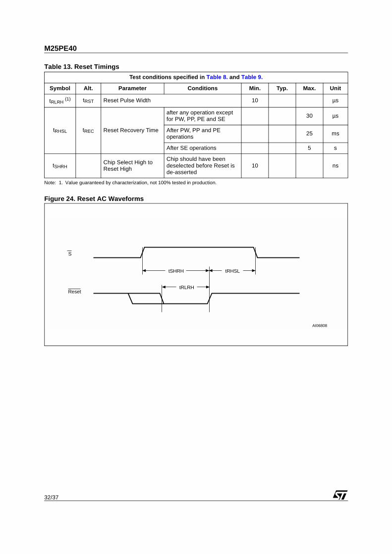
Table 13. Reset Timings
Note: 1. Value guaranteed by characterization, not 100% tested in production.
Figure 24. Reset AC Waveforms
Test conditions specified in Table 8. and Table 9.
Symbol Alt. Parameter Conditions Min. Typ. Max. Unit
tRLRH (1) tRST Reset Pulse Width 10 µs
tRHSL tREC Reset Recovery Time
after any operation except for PW, PP, PE and SE
30 µs
After PW, PP and PE operations
25 ms
After SE operations 5 s
tSHRHChip Select High to Reset High
Chip should have been deselected before Reset is de-asserted
10 ns
AI06808
ResettRLRH
S
tRHSLtSHRH
33/37
M25PE40
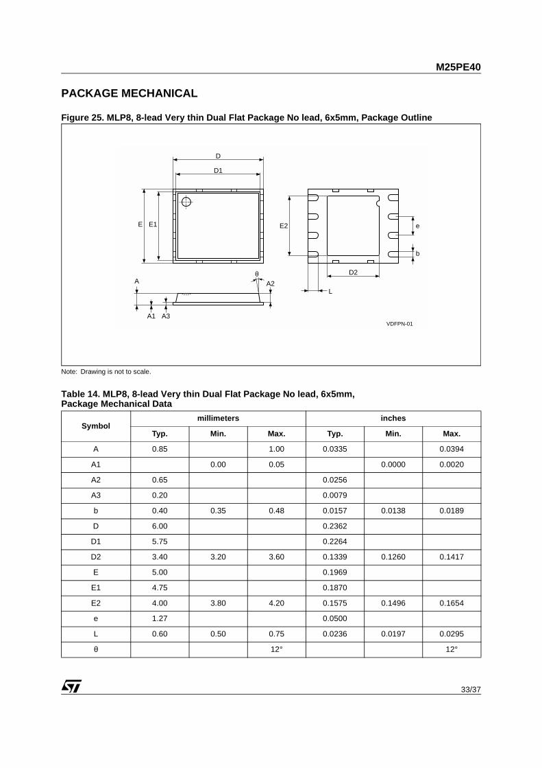
PACKAGE MECHANICAL
Figure 25. MLP8, 8-lead Very thin Dual Flat Package No lead, 6x5mm, Package Outline
Note: Drawing is not to scale.
Table 14. MLP8, 8-lead Very thin Dual Flat Package No lead, 6x5mm, Package Mechanical Data
Symbolmillimeters inches
Typ. Min. Max. Typ. Min. Max.
A 0.85 1.00 0.0335 0.0394
A1 0.00 0.05 0.0000 0.0020
A2 0.65 0.0256
A3 0.20 0.0079
b 0.40 0.35 0.48 0.0157 0.0138 0.0189
D 6.00 0.2362
D1 5.75 0.2264
D2 3.40 3.20 3.60 0.1339 0.1260 0.1417
E 5.00 0.1969
E1 4.75 0.1870
E2 4.00 3.80 4.20 0.1575 0.1496 0.1654
e 1.27 0.0500
L 0.60 0.50 0.75 0.0236 0.0197 0.0295
θ 12° 12°
D
E
VDFPN-01
A2A
A3A1
E1
D1
eE2
D2
L
b
θ
M25PE40
34/37
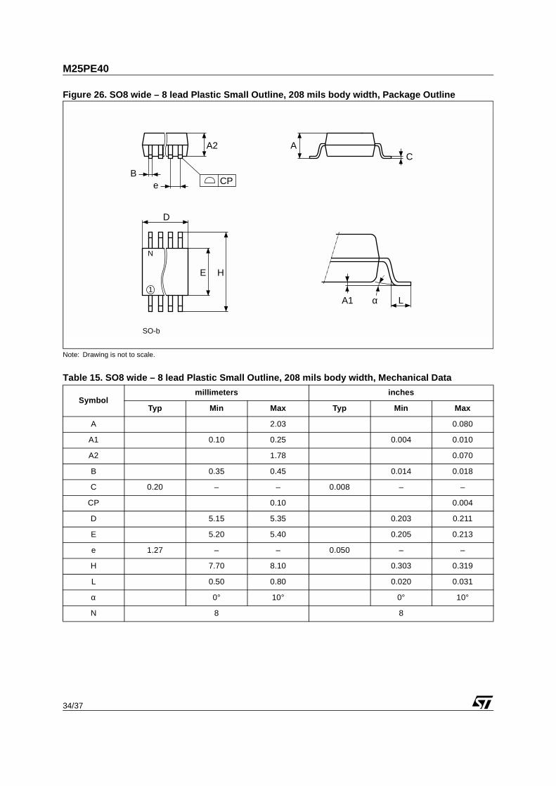
Figure 26. SO8 wide – 8 lead Plastic Small Outline, 208 mils body width, Package Outline
Note: Drawing is not to scale.
Table 15. SO8 wide – 8 lead Plastic Small Outline, 208 mils body width, Mechanical Data
Symbolmillimeters inches
Typ Min Max Typ Min Max
A 2.03 0.080
A1 0.10 0.25 0.004 0.010
A2 1.78 0.070
B 0.35 0.45 0.014 0.018
C 0.20 – – 0.008 – –
CP 0.10 0.004
D 5.15 5.35 0.203 0.211
E 5.20 5.40 0.205 0.213
e 1.27 – – 0.050 – –
H 7.70 8.10 0.303 0.319
L 0.50 0.80 0.020 0.031
α 0° 10° 0° 10°
N 8 8
SO-b
E
N
CPB
e
A2
D
C
LA1 α
H
A
1
35/37
M25PE40
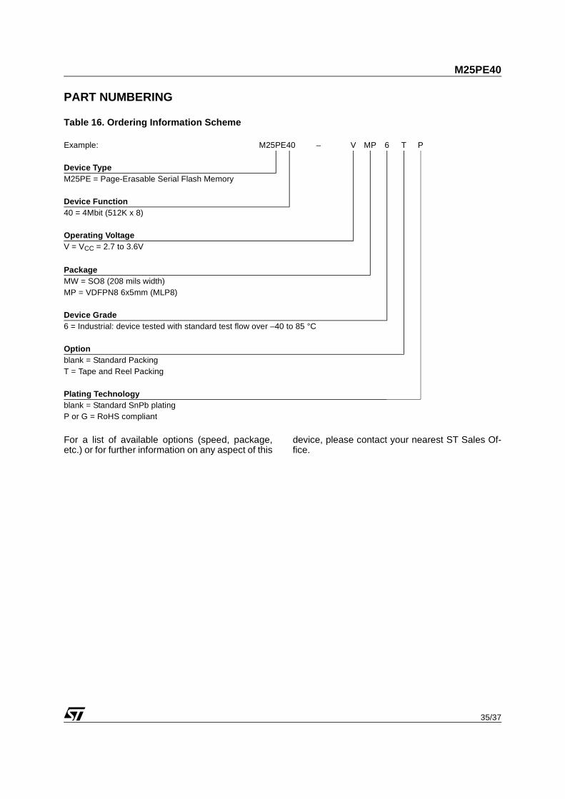
PART NUMBERING
Table 16. Ordering Information Scheme
For a list of available options (speed, package,etc.) or for further information on any aspect of this
device, please contact your nearest ST Sales Of-fice.
Example: M25PE40 – V MP 6 T P
Device TypeM25PE = Page-Erasable Serial Flash Memory
Device Function40 = 4Mbit (512K x 8)
Operating VoltageV = VCC = 2.7 to 3.6V
PackageMW = SO8 (208 mils width)MP = VDFPN8 6x5mm (MLP8)
Device Grade6 = Industrial: device tested with standard test flow over –40 to 85 °C
Optionblank = Standard PackingT = Tape and Reel Packing
Plating Technologyblank = Standard SnPb platingP or G = RoHS compliant
M25PE40
36/37
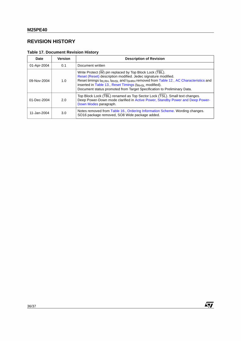
REVISION HISTORY
Table 17. Document Revision History
Date Version Description of Revision
01-Apr-2004 0.1 Document written
09-Nov-2004 1.0
Write Protect (W) pin replaced by Top Block Lock (TBL). Reset (Reset) description modified. Jedec signature modified. Reset timings tRLRH, tRHSL and tSHRH removed from Table 12., AC Characteristics and inserted in Table 13., Reset Timings (tRHSL modified).Document status promoted from Target Specification to Preliminary Data.
01-Dec-2004 2.0Top Block Lock (TBL) renamed as Top Sector Lock (TSL). Small text changes.Deep Power-Down mode clarified in Active Power, Standby Power and Deep Power-Down Modes paragraph.
11-Jan-2004 3.0Notes removed from Table 16., Ordering Information Scheme. Wording changes. SO16 package removed, SO8 Wide package added.
37/37
M25PE40
Information furnished is believed to be accurate and reliable. However, STMicroelectronics assumes no responsibility for the consequences of use of such information nor for any infringement of patents or other rights of third parties which may result from its use. No license is granted by implication or otherwise under any patent or patent rights of STMicroelectronics. Specifications mentioned in this publication are subject to change without notice. This publication supersedes and replaces all information previously supplied. STMicroelectronics products are not
authorized for use as critical components in life support devices or systems without express written approval of STMicroelectronics.
The ST logo is a registered trademark of STMicroelectronics.ECOPACK is a registered trademark of STMicroelectronics.All other names are the property of their respective owners
© 2005 STMicroelectronics - All rights reserved
STMicroelectronics group of companiesAustralia - Belgium - Brazil - Canada - China - Czech Republic - Finland - France - Germany - Hong Kong - India - Israel - Italy - Japan -
Malaysia - Malta - Morocco - Singapore - Spain - Sweden - Switzerland - United Kingdom - United States of Americawww.st.com