3.3v dual-speed fast ethernet transceiver datasheetcardoso/ie344b/lxt972a.pdf · 3.3v dual-speed...
TRANSCRIPT

Intel® LXT972A3.3V Dual-Speed Fast Ethernet Transceiver Datasheet
DatasheetThe LXT972A is an IEEE compliant Fast Ethernet PHY Transceiver that directly supports both 100BASE-TX and 10BASE-T applications. It provides a Media Independent Interface (MII) for easy attachment to 10/100 Media Access Controllers (MACs).
This document also supports the LXT972.
The LXT972A supports full-duplex operation at 10 Mbps and 100 Mbps. Its operating condition can be set using auto-negotiation, parallel detection, or manual control.
The LXT972A is fabricated with an advanced CMOS process and requires only a single 3.3 V power supply.
Applications
Product Features
Combination 10BASE-T/100BASE-TX Network Interface Cards (NICs)
10/100 PCMCIA Cards Cable Modems and Set-Top Boxes
3.3 V Operation. Low power consumption (300 mW
typical). 10BASE-T and 100BASE-TX using a
single RJ-45 connection. Supports auto-negotiation and parallel
detection. MII interface with extended register
capability. Robust baseline wander correction
performance. Supports JTAG Boundary Scan
Standard CSMA/CD or full-duplex operation.
Configurable via MDIO serial port or hardware control pins.
Integrated, programmable LED drivers. 64-pin Low-profile Quad Flat Package
(LQFP). —LXT972ALC - Commercial (0° to 70°C
ambient).
Order Number: 249186-003. August 2002

2
INFORMATION IN TESTOPPEL OR OTHTERMS AND CONDEXPRESS OR IMPLRELATING TO FITNINTELLECTUAL PR
Intel may make chang
Designers must not reand shall have no resp
The LXT972A may cerrata are available on
Contact your local In
Copies of documents1-800-548-4725 or by
Copyright © Intel Co
*Third-party brands a
DatasheetDocument #: 249186
Revision #: 003Rev. Date: August 7, 2002
HIS DOCUMENT IS PROVIDED IN CONNECTION WITH INTELÆ PRODUCTS. NO LICENSE, EXPRESS OR IMPLIED, BY ERWISE, TO ANY INTELLECTUAL PROPERTY RIGHTS IS GRANTED BY THIS DOCUMENT. EXCEPT AS PROVIDED IN INTEL'S ITIONS OF SALE FOR SUCH PRODUCTS, INTEL ASSUMES NO LIABILITY WHATSOEVER, AND INTEL DISCLAIMS ANY
IED WARRANTY, RELATING TO SALE AND/OR USE OF INTEL PRODUCTS INCLUDING LIABILITY OR WARRANTIES ESS FOR A PARTICULAR PURPOSE, MERCHANTABILITY, OR INFRINGEMENT OF ANY PATENT, COPYRIGHT OR OTHER OPERTY RIGHT. Intel products are not intended for use in medical, life saving, life sustaining applications.
es to specifications and product descriptions at any time, without notice.
ly on the absence or characteristics of any features or instructions marked "reserved" or "undefined." Intel reserves these for future definition onsibility whatsoever for conflicts or incompatibilities arising from future changes to them.
ontain design defects or errors known as errata which may cause the product to deviate from published specifications. Current characterized request.
tel sales office or your distributor to obtain the latest specifications and before placing your product order.
which have an ordering number and are referenced in this document, or other Intel literature may be obtained by calling visiting Intel's website at http://www.intel.com.
rporation, 2002
nd names are the property of their respective owners.

LXT972A 3.3 V Dual-Speed Fast Ethernet Transceiver
Contents1.0 Pin Assignments .............................................................................................................................10
2.0 Signal Descriptions ........................................................................................................................13
3.0 Functional Description ..................................................................................................................173.1 Introduction .......................................................................................................................17
3.1.1 Comprehensive Functionality .............................................................................173.1.2 OSP™ Architecture ............................................................................................17
3.2 Network Media / Protocol Support....................................................................................183.2.1 10/100 Network Interface ...................................................................................18
3.2.1.1 Twisted-Pair Interface ..........................................................................183.2.1.2 Fault Detection and Reporting..............................................................18
3.2.2 MII Data Interface...............................................................................................193.2.2.1 Increased MII Drive Strength ...............................................................19
3.2.3 Configuration Management Interface .................................................................193.2.3.1 MDIO Management Interface ..............................................................193.2.3.2 MII Interrupts .......................................................................................203.2.3.3 Hardware Control Interface ..................................................................20
3.3 Operating Requirements....................................................................................................213.3.1 Power Requirements ...........................................................................................213.3.2 Clock Requirements............................................................................................21
3.3.2.1 External Crystal/Oscillator ...................................................................213.3.2.2 MDIO Clock .........................................................................................21
3.4 Initialization.......................................................................................................................223.4.1 MDIO Control Mode ..........................................................................................223.4.2 Hardware Control Mode .....................................................................................223.4.3 Reduced Power Modes........................................................................................23
3.4.3.1 Hardware Power Down ........................................................................233.4.3.2 Software Power Down..........................................................................24
3.4.4 Reset....................................................................................................................243.4.5 Hardware Configuration Settings........................................................................24
3.5 Establishing Link...............................................................................................................253.5.1 Auto-Negotiation ................................................................................................25
3.5.1.1 Base Page Exchange .............................................................................253.5.1.2 Next Page Exchange .............................................................................253.5.1.3 Controlling Auto-Negotiation...............................................................26
3.5.2 Parallel Detection................................................................................................263.6 MII Operation....................................................................................................................26
3.6.1 MII Clocks ..........................................................................................................273.6.2 Transmit Enable ..................................................................................................273.6.3 Receive Data Valid .............................................................................................273.6.4 Carrier Sense .......................................................................................................273.6.5 Error Signals .......................................................................................................273.6.6 Collision ..............................................................................................................273.6.7 Loopback.............................................................................................................29
3.6.7.1 Operational Loopback ..........................................................................293.6.7.2 Test Loopback ......................................................................................29
Datasheet 3Document #: 249186Revision #: 003Rev. Date: August 7, 2002

LXT972A 3.3 V Dual-Speed Fast Ethernet Transceiver
3.7 100 Mbps Operation ......................................................................................................... 303.7.1 100BASE-X Network Operations...................................................................... 303.7.2 Collision Indication ............................................................................................ 323.7.3 100BASE-X Protocol Sublayer Operations ....................................................... 32
3.7.3.1 PCS Sublayer ....................................................................................... 333.7.3.2 PMA Sublayer...................................................................................... 353.7.3.3 Twisted-Pair PMD Sublayer ................................................................ 36
3.8 10 Mbps Operation ........................................................................................................... 363.8.1 10BASE-T Preamble Handling.......................................................................... 373.8.2 10BASE-T Carrier Sense ................................................................................... 373.8.3 10BASE-T Dribble Bits ..................................................................................... 373.8.4 10BASE-T Link Integrity Test........................................................................... 37
3.8.4.1 Link Failure.......................................................................................... 373.8.5 10T SQE (Heartbeat).......................................................................................... 383.8.6 10T Jabber .......................................................................................................... 383.8.7 10T Polarity Correction...................................................................................... 38
3.9 Monitoring Operations ..................................................................................................... 383.9.1 Monitoring Auto-Negotiation ............................................................................ 38
3.9.1.1 Monitoring Next Page Exchange......................................................... 383.9.2 LED Functions ................................................................................................... 39
3.9.2.1 LED Pulse Stretching........................................................................... 393.10 Boundary Scan (JTAG1149.1) Functions ........................................................................ 40
3.10.1 Boundary Scan Interface .................................................................................... 403.10.2 State Machine.................................................................................................... 403.10.3 Instruction Register ............................................................................................ 403.10.4 Boundary Scan Register (BSR).......................................................................... 40
4.0 Application Information ............................................................................................................... 424.1 Magnetics Information ..................................................................................................... 424.2 Typical Twisted-Pair Interface ......................................................................................... 42
5.0 Test Specifications......................................................................................................................... 455.1 Electrical Parameters ........................................................................................................ 455.2 Timing Diagrams.............................................................................................................. 49
6.0 Register Definitions....................................................................................................................... 57
7.0 Package Specification ................................................................................................................... 73
8.0 Product Ordering Information .................................................................................................... 74
4 DatasheetDocument #: 249186
Revision #: 003Rev. Date: August 7, 2002

LXT972A 3.3 V Dual-Speed Fast Ethernet Transceiver
Figures1 LXT972A Block Diagram...................................................................................................92 LXT972A 64-Pin LQFP Assignments ..............................................................................103 Management Interface Read Frame Structure ..................................................................204 Management Interface Write Frame Structure .................................................................205 Interrupt Logic ..................................................................................................................216 Initialization Sequence .....................................................................................................237 Hardware Configuration Settings .....................................................................................248 Link Establishment Overview ..........................................................................................269 10BASE-T Clocking ........................................................................................................2810 100BASE-X Clocking ......................................................................................................2811 Link Down Clock Transition ............................................................................................2812 Loopback Paths ................................................................................................................2913 100BASE-X Frame Format ..............................................................................................3014 100BASE-TX Data Path ...................................................................................................3115 100BASE-TX Reception with no Errors ..........................................................................3116 100BASE-TX Reception with Invalid Symbol ................................................................3217 100BASE-TX Transmission with no Errors .....................................................................3218 100BASE-TX Transmission with Collision .....................................................................3219 Protocol Sublayers ............................................................................................................3320 LED Pulse Stretching .......................................................................................................4021 Typical Twisted-Pair Interface - Switch............................................................................4322 Typical Twisted-Pair Interface - NIC ...............................................................................4423 Typical MII Interface .......................................................................................................4424 100BASE-TX Receive Timing - 4B Mode ......................................................................4925 100BASE-TX Transmit Timing - 4B Mode .....................................................................5026 10BASE-T Receive Timing .............................................................................................5127 10BASE-T Transmit Timing ............................................................................................5228 10BASE-T Jabber and Unjabber Timing .........................................................................5329 10BASE-T SQE (Heartbeat) Timing ................................................................................5330 Auto Negotiation and Fast Link Pulse Timing .................................................................5431 Fast Link Pulse Timing ....................................................................................................5432 MDIO Input Timing .........................................................................................................5533 MDIO Output Timing .......................................................................................................5534 Power-Up Timing .............................................................................................................5635 RESET Pulse Width and Recovery Timing .....................................................................5636 PHY Identifier Bit Mapping .............................................................................................6237 LXT972A LQFP Package Specifications .........................................................................7338 Ordering Information - Sample .........................................................................................74
Tables1 LQFP Numeric Pin List....................................................................................................112 LXT972A MII Signal Descriptions...................................................................................133 LXT972A Network Interface Signal Descriptions............................................................144 LXT972A Miscellaneous Signal Descriptions..................................................................145 LXT972A Power Supply Signal Descriptions ..................................................................156 LXT972A JTAG Test Signal Descriptions .......................................................................157 LXT972A LED Signal Descriptions .................................................................................16
Datasheet 5Document #: 249186Revision #: 003Rev. Date: August 7, 2002

LXT972A 3.3 V Dual-Speed Fast Ethernet Transceiver
8 LXT972A Pin Types and Modes...................................................................................... 169 Hardware Configuration Settings ..................................................................................... 2510 Carrier Sense, Loopback, and Collision Conditions......................................................... 2911 4B/5B Coding ................................................................................................................... 3412 BSR Mode of Operation ................................................................................................... 4113 Supported JTAG Instructions ........................................................................................... 4114 Device ID Register ........................................................................................................... 4115 Magnetics Requirements .................................................................................................. 4216 RJ-45 Pin Comparison of NIC and Switch Twisted-Pair Interfaces ................................ 4217 Absolute Maximum Ratings ............................................................................................. 4518 Operating Conditions........................................................................................................ 4519 Digital I/O Characteristics1 .............................................................................................. 4620 Digital I/O Characteristics - MII Pins............................................................................... 4621 I/O Characteristics - REFCLK/XI and XO Pins............................................................... 4622 I/O Characteristics - LED/CFG Pins ................................................................................ 4723 100BASE-TX Transceiver Characteristics....................................................................... 4724 10BASE-T Transceiver Characteristics............................................................................ 4725 10BASE-T Link Integrity Timing Characteristics ........................................................... 4826 LXT972A Thermal Characteristics .................................................................................. 4827 100BASE-TX Receive Timing Parameters - 4B Mode.................................................... 4928 100BASE-TX Transmit Timing Parameters - 4B Mode .................................................. 5029 10BASE-T Receive Timing Parameters........................................................................... 5130 10BASE-T Transmit Timing Parameters ......................................................................... 5231 10BASE-T Jabber and Unjabber Timing Parameters....................................................... 5332 10BASE-T SQE Timing Parameters ................................................................................ 5333 Auto Negotiation and Fast Link Pulse Timing Parameters .............................................. 5434 MDIO Timing Parameters ................................................................................................ 5535 Power-Up Timing Parameters ......................................................................................... 5636 RESET Pulse Width and Recovery Timing Parameters.................................................. 5637 Register Set....................................................................................................................... 5738 Register Bit Map............................................................................................................... 5839 Control Register (Address 0) ............................................................................................ 6040 MII Status Register #1 (Address 1) .................................................................................. 6141 PHY Identification Register 1 (Address 2)....................................................................... 6242 PHY Identification Register 2 (Address 3)....................................................................... 6243 Auto Negotiation Advertisement Register (Address 4).................................................... 6344 Auto Negotiation Link Partner Base Page Ability Register (Address 5) ......................... 6445 Auto Negotiation Expansion (Address 6)......................................................................... 6546 Auto Negotiation Next Page Transmit Register (Address 7) ........................................... 6547 Auto Negotiation Link Partner Next Page Receive Register (Address 8)........................ 6648 Configuration Register (Address 16, Hex 10) .................................................................. 6649 Status Register #2 (Address 17) ....................................................................................... 6750 Interrupt Enable Register (Address 18) ............................................................................ 6851 Interrupt Status Register (Address 19, Hex 13)................................................................ 6852 LED Configuration Register (Address 20, Hex 14) ......................................................... 7053 Digital Config Register (Address 26) ............................................................................... 7154 Transmit Control Register #2 (Address 30) ..................................................................... 7255 Product Information.......................................................................................................... 74
6 DatasheetDocument #: 249186
Revision #: 003Rev. Date: August 7, 2002

LXT972A 3.3 V Dual-Speed Fast Ethernet Transceiver
Revision HistoryRevision 003
Revision Date: August 6, 2002
Page # Description
1 Added “JTAG Boundary Scan” to Product Features on front page.
10 Modified Figure 2 “LXT972A 64-Pin LQFP Assignments” (replaced TEST1 and TEST0 with GND).
11 Modified Table 1 “LQFP Numeric Pin List” (replaced TEST1 and TEST0 with GND).
13 Added note under Section 2.0, “Signal Descriptions”: “Intel recommends that all inputs and multi-function pins be tied to the inactive states and all outputs be left floating, if unused.”
14 Modified Table 4 “LXT972A Miscellaneous Signal Descriptions”.
15 Modified Table 5 “LXT972A Power Supply Signal Descriptions”.
16 Added Table 8 “LXT972A Pin Types and Modes”.
19 Added Section 3.2.2.1, “Increased MII Drive Strength”.
24 Modified Figure 7 “Hardware Configuration Settings”.
41 Modified Table 13 “Supported JTAG Instructions”.
41 Modified Table 14 “Device ID Register”.
45 Modified Table 17 “Absolute Maximum Ratings”.
45 Modified Table 18 “Operating Conditions”: Added Typ values to Vcc current.
46 Modified Table 20 “Digital I/O Characteristics - MII Pins”.
47 Modified Table 22 “I/O Characteristics - LED/CFG Pins”.
48 Added Table 26 “LXT972A Thermal Characteristics”.
51 Modified Table 29 “10BASE-T Receive Timing Parameters”.
58 Modified Table 38 “Register Bit Map” (added Address 26 information).
71 Added Table 53 “Digital Config Register (Address 26)”.
72 Modified Table 54 “Transmit Control Register #2 (Address 30)”.
74 Added Section 8.0, “Product Ordering Information”.
Revision 002Revision Date: January 2001
Page # Description
N/A Clock Requirements: Modified language under Clock Requirements heading.
I/O Characteristics REFCLK (table): Changed values for Input Clock Duty Cycle under Min from 40 to 35 and under Max from 60 to 65.
Datasheet 7Document #: 249186Revision #: 003Rev. Date: August 7, 2002

LXT972A 3.3 V Dual-Speed Fast Ethernet Transceiver
8 DatasheetDocument #: 249186
Revision #: 003Rev. Date: August 7, 2002

LXT972A 3.3 V Dual-Speed Fast Ethernet Transceiver
Figure 1. LXT972A Block Diagram
TX_EN
RX_ER
CRS
Pwr SupplyManagement /Mode Select
Logic
ADDR0MDIOMDC
MDINT
TX_ER
RXDV
TPON
TPOP
TPIN
TPIP
REFCLK
VCCGND
COL
RX_CLK
TX_CLK
RESET
LED/CFG<3:1>
TXD<3:0>
Decoder &Descrambler
+
-
Serial-to-Parallel
Converter
Scrambler& Encoder
Parallel/SerialConverter
Carrier SenseData Valid
Error Detect
AutoNegotiation
ManchesterDecoder
ManchesterEncoder 10
100
10
100
MediaSelect
TPDriver
TP Out
RegisterSet
Register SetClock
Generator
+
-10BT
CollisionDetect Clock
Generator
TX P
CS
OSP™Adaptive EQ withBaseline Wander
Cancellation
OSP™Slicer
OSP™Pulse
Shaper
RXD<3:0>
+
-100TX
TP In
MDDISTxSLEW<1:0>
RX
PCS
PWRDWN
JTAG
TDI,TDO,TMS,TCK,TRST
Datasheet 9Document #: 249186Revision #: 003Rev. Date: August 7, 2002

LXT972A 3.3 V Dual-Speed Fast Ethernet Transceiver
1.0 Pin Assignments
Figure 2. LXT972A 64-Pin LQFP Assignments
Package Topside Markings
Marking Definition
Part # LXT972A is the unique identifier for this product family.
Rev # Identifies the particular silicon “stepping” (Refer to Specification Update for additional stepping information.)
Lot # Identifies the batch.
FPO # Identifies the Finish Process Order.
RXD0R
BIA
S17
6412345678910111213141516
REFCLK/XIXO
MDDISRESET
TXSLEW0TXSLEW1
GNDVCCIO
N/CN/C
GNDADDR0
GNDGNDGNDGND
18 19 20 21 22 23 24 25 26 27 28 29 30 31 32
GN
DTP
OP
TPO
NV
CC
AV
CC
ATP
IPTP
ING
ND
GN
DTD
ITD
OTM
STC
KTR
STG
ND
474645444342414039383736353433
RXD1RXD2RXD3N/CMDCMDIOGNDVCCIOPWRDWNLED/CFG1LED/CFG2LED/CFG3GNDGNDPAUSE
MD
INT
CR
SC
OL
GN
DTX
D3
TXD
2TX
D1
TXD
0TX
_EN
TX_C
LKTX
_ER
RX
_ER
RX
_CLK
VC
CD
GN
DR
X_D
V
63 62 61 60 59 58 57 56 55 54 53 52 51 50 49
48
LXT972A XXXXXXXXXXXXXXXX
Part #LOT #FPO #
Rev #
10 DatasheetDocument #: 249186
Revision #: 003Rev. Date: August 7, 2002

LXT972A 3.3 V Dual-Speed Fast Ethernet Transceiver
Table 1. LQFP Numeric Pin List
Pin Symbol Type Reference forFull Description
1 REFCLK/XI Input Table 4 on page 14
2 XO Output Table 4 on page 14
3 MDDIS Input Table 2 on page 13
4 RESET Input Table 4 on page 14
5 TxSLEW0 Input Table 4 on page 14
6 TxSLEW1 Input Table 4 on page 14
7 GND – Table 5 on page 15
8 VCCIO – Table 5 on page 15
9 N/C – Table 4 on page 14
10 N/C – Table 4 on page 14
11 GND – Table 5 on page 15
12 ADDR0 Input Table 4 on page 14
13 GND – Table 5 on page 15
14 GND – Table 5 on page 15
15 GND – Table 5 on page 15
16 GND – Table 5 on page 15
17 RBIAS Analog Input Table 4 on page 14
18 GND – Table 5 on page 15
19 TPOP Output Table 3 on page 14
20 TPON Output Table 3 on page 14
21 VCCA – Table 5 on page 15
22 VCCA – Table 5 on page 15
23 TPIP Input Table 3 on page 14
24 TPIN Input Table 3 on page 14
25 GND – Table 5 on page 15
26 GND – Table 5 on page 15
27 TDI Input Table 6 on page 15
28 TDO Output Table 6 on page 15
29 TMS Input Table 6 on page 15
30 TCK Input Table 6 on page 15
31 TRST Input Table 6 on page 15
32 GND – Table 5 on page 15
33 PAUSE Input Table 4 on page 14
34 GND – Table 4 on page 14
35 GND – Table 4 on page 14
36 LED/CFG3 I/O Table 7 on page 16
Datasheet 11Document #: 249186Revision #: 003Rev. Date: August 7, 2002

LXT972A 3.3 V Dual-Speed Fast Ethernet Transceiver
37 LED/CFG2 I/O Table 7 on page 16
38 LED/CFG1 I/O Table 7 on page 16
39 PWRDWN Input Table 4 on page 14
40 VCCIO – Table 5 on page 15
41 GND – Table 5 on page 15
42 MDIO I/O Table 2 on page 13
43 MDC Input Table 2 on page 13
44 N/C – Table 4 on page 14
45 RXD3 Output Table 2 on page 13
46 RXD2 Output Table 2 on page 13
47 RXD1 Output Table 2 on page 13
48 RXD0 Output Table 2 on page 13
49 RX_DV Output Table 2 on page 13
50 GND – Table 5 on page 15
51 VCCD – Table 5 on page 15
52 RX_CLK Output Table 2 on page 13
53 RX_ER Output Table 2 on page 13
54 TX_ER Input Table 2 on page 13
55 TX_CLK Output Table 2 on page 13
56 TX_EN Input Table 2 on page 13
57 TXD0 Input Table 2 on page 13
58 TXD1 Input Table 2 on page 13
59 TXD2 Input Table 2 on page 13
60 TXD3 Input Table 2 on page 13
61 GND – Table 5 on page 15
62 COL Output Table 2 on page 13
63 CRS Output Table 2 on page 13
64 MDINT Open Drain Table 2 on page 13
Table 1. LQFP Numeric Pin List (Continued)
Pin Symbol Type Reference forFull Description
12 DatasheetDocument #: 249186
Revision #: 003Rev. Date: August 7, 2002
LXT972A 3.3 V Dual-Speed Fast Ethernet Transceiver
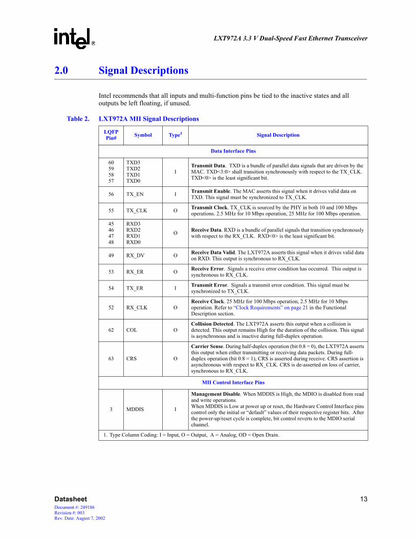
2.0 Signal Descriptions
Intel recommends that all inputs and multi-function pins be tied to the inactive states and all outputs be left floating, if unused.
Table 2. LXT972A MII Signal Descriptions
LQFPPin# Symbol Type1 Signal Description
Data Interface Pins
60595857
TXD3TXD2TXD1TXD0
ITransmit Data. TXD is a bundle of parallel data signals that are driven by the MAC. TXD<3:0> shall transition synchronously with respect to the TX_CLK. TXD<0> is the least significant bit.
56 TX_EN I Transmit Enable. The MAC asserts this signal when it drives valid data on TXD. This signal must be synchronized to TX_CLK.
55 TX_CLK O Transmit Clock. TX_CLK is sourced by the PHY in both 10 and 100 Mbps operations. 2.5 MHz for 10 Mbps operation, 25 MHz for 100 Mbps operation.
45464748
RXD3RXD2RXD1RXD0
O Receive Data. RXD is a bundle of parallel signals that transition synchronously with respect to the RX_CLK. RXD<0> is the least significant bit.
49 RX_DV O Receive Data Valid. The LXT972A asserts this signal when it drives valid data on RXD. This output is synchronous to RX_CLK.
53 RX_ER O Receive Error. Signals a receive error condition has occurred. This output is synchronous to RX_CLK.
54 TX_ER I Transmit Error. Signals a transmit error condition. This signal must be synchronized to TX_CLK.
52 RX_CLK OReceive Clock. 25 MHz for 100 Mbps operation, 2.5 MHz for 10 Mbps operation. Refer to “Clock Requirements” on page 21 in the Functional Description section.
62 COL OCollision Detected. The LXT972A asserts this output when a collision is detected. This output remains High for the duration of the collision. This signal is asynchronous and is inactive during full-duplex operation.
63 CRS O
Carrier Sense. During half-duplex operation (bit 0.8 = 0), the LXT972A asserts this output when either transmitting or receiving data packets. During full-duplex operation (bit 0.8 = 1), CRS is asserted during receive. CRS assertion is asynchronous with respect to RX_CLK. CRS is de-asserted on loss of carrier, synchronous to RX_CLK.
MII Control Interface Pins
3 MDDIS I
Management Disable. When MDDIS is High, the MDIO is disabled from read and write operations.When MDDIS is Low at power up or reset, the Hardware Control Interface pins control only the initial or “default” values of their respective register bits. After the power-up/reset cycle is complete, bit control reverts to the MDIO serial channel.
1. Type Column Coding: I = Input, O = Output, A = Analog, OD = Open Drain.
Datasheet 13Document #: 249186Revision #: 003Rev. Date: August 7, 2002

LXT972A 3.3 V Dual-Speed Fast Ethernet Transceiver
43 MDC I Management Data Clock. Clock for the MDIO serial data channel. Maximum frequency is 8 MHz.
42 MDIO I/O Management Data Input/Output. Bidirectional serial data channel for PHY/STA communication.
64 MDINT OD Management Data Interrupt. When bit 18.1 = 1, an active Low output on this pin indicates status change. Interrupt is cleared by reading Register 19.
Table 3. LXT972A Network Interface Signal Descriptions
LQFPPin# Symbol Type1 Signal Description
1920
TPOPTPON
OTwisted-Pair Outputs, Positive & Negative.During 100BASE-TX or 10BASE-T operation, TPOP/N pins drive 802.3 compliant pulses onto the line.
2324
TPIPTPIN
ITwisted-Pair Inputs, Positive & Negative.During 100BASE-TX or 10BASE-T operation, TPIP/N pins receive differential 100BASE-TX or 10BASE-T signals from the line.
1. Type Column Coding: I = Input, O = Output, A = Analog, OD = Open Drain
Table 4. LXT972A Miscellaneous Signal Descriptions
LQFPPin# Symbol Type1 Signal Description
56
TxSLEW0TxSLEW1
I
Tx Output Slew Controls 0 and 1. These pins select the TX output slew rate (rise and fall time) as follows:
TxSLEW1 TxSLEW0 Slew Rate (Rise and Fall Time)
0 0 3.0 ns
0 1 3.4 ns
1 0 3.9 ns
1 1 4.4 ns
4 RESET IReset. This active Low input is OR’ed with the control register Reset bit (0.15). The LXT972A reset cycle is extended to 258 µs (nominal) after reset is deasserted.
12 ADDR0 I Address0. Sets device address.
17 RBIAS AI Bias. This pin provides bias current for the internal circuitry. Must be tied to ground through a 22.1 kΩ, 1% resistor.
33 PAUSE I Pause. When set High, the LXT972A advertises Pause capabilities during auto negotiation.
1. Type Column Coding: I = Input, O = Output, A = Analog, OD = Open Drain
Table 2. LXT972A MII Signal Descriptions (Continued)
LQFPPin# Symbol Type1 Signal Description
1. Type Column Coding: I = Input, O = Output, A = Analog, OD = Open Drain.
14 DatasheetDocument #: 249186
Revision #: 003Rev. Date: August 7, 2002

LXT972A 3.3 V Dual-Speed Fast Ethernet Transceiver
39 PWRDWN I Power Down. When set High, this pin puts the LXT972A in a power-down mode.
12
REFCLK/XIXO
IO
Crystal Input and Output. A 25 MHz crystal oscillator circuit can be connected across XI and XO. A clock can also be used at XI. Refer to Functional Description for detailed clock requirements.
9, 10,44
N/C - No Connection. These pins are not used and should not be terminated.
Table 5. LXT972A Power Supply Signal Descriptions
LQFPPin# Symbol Type Signal Description
51 VCCD - Digital Power. Requires a 3.3 V power supply.
7, 11, 13, 14, 15, 16, 18, 25, 26, 32, 34, 35, 41, 50, 61
GND - Ground.
8, 40 VCCIO - MII Power. Requires either a 3.3 V or a 2.5 V supply. Must be supplied from the same source used to power the MAC on the other side of the MII.
21, 22 VCCA - Analog Power. Requires a 3.3 V power supply.
Table 6. LXT972A JTAG Test Signal Descriptions
LQFPPin# Symbol Type1 Signal Description
27 TDI2 I Test Data Input. Test data sampled with respect to the rising edge of TCK.
28 TDO2 O Test Data Output. Test data driven with respect to the falling edge of TCK.
29 TMS2 I Test Mode Select.
30 TCK2 I Test Clock. Test clock input sourced by ATE.
31 TRST2 I Test Reset. Test reset input sourced by ATE.
1. Type Column Coding: I = Input, O = Output, A = Analog, OD = Open Drain.2. If JTAG port is not used, these pins do not need to be terminated.
Table 7. LXT972A LED Signal Descriptions
LQFPPin# Symbol Type1 Signal Description
383736
LED/CFG1LED/CFG2LED/CFG3
I/O
LED Drivers 1 -3. These pins drive LED indicators. Each LED can display one of several available status conditions as selected by the LED Configuration Register (refer to Table 52 on page 70 for details).Configuration Inputs 1-3. These pins also provide initial configuration settings (refer to Table 9 on page 25 for details).
1. Type Column Coding: I = Input, O = Output, A = Analog, OD = Open Drain
Table 4. LXT972A Miscellaneous Signal Descriptions (Continued)
LQFPPin# Symbol Type1 Signal Description
1. Type Column Coding: I = Input, O = Output, A = Analog, OD = Open Drain
Datasheet 15Document #: 249186Revision #: 003Rev. Date: August 7, 2002

LXT972A 3.3 V Dual-Speed Fast Ethernet Transceiver
Table 8. LXT972A Pin Types and Modes
Modes RXD 0-3 RXDVTx/Rx CLKS
OutputRXER Output
COL Output
CRS Output
TXD 0-3 Input
TXEN Input
TXER Input
HWReset DL DL DH DL DL DL IPLD IPLD IPLD
SFTPWRDN DL DL Active DL DL DL IPLD IPLD IPLD
HWPWRDN High Z High Z High Z High Z High Z High Z High Z High Z High Z
ISOLATE HZ w/IPLD
HZ w/IPLD
HZ w/IPLD
HZ w/IPLD
HZ w/IPLD
HZ w/IPLD IPLD IPLD IPLD
1. A High Z (High impedance) or three state determines when the device is drawing a current of less than 20 nA. A High Z with PLD (High impedance with pull-down) state determines when the device is drawing a current of less than 20 uA.
2. DL = Driven Low (Logic 0), DH = Driven High (Logic 1), IPLD = Internal Pull-Down (Weak)
16 DatasheetDocument #: 249186
Revision #: 003Rev. Date: August 7, 2002

LXT972A 3.3 V Dual-Speed Fast Ethernet Transceiver
3.0 Functional Description
3.1 Introduction
The LXT972A is a single-port Fast Ethernet 10/100 Transceiver that supports 10 Mbps and 100 Mbps networks. It complies with all applicable requirements of IEEE 802.3. The LXT972A can directly drive either a 100BASE-TX line (up to 140 meters) or a 10BASE-T line (up to 185 meters).
3.1.1 Comprehensive Functionality
The LXT972A provides a standard Media Independent Interface (MII) for 10/100 MACs. The LXT972A performs all functions of the Physical Coding Sublayer (PCS) and Physical Media Attachment (PMA) sublayer as defined in the IEEE 802.3 100BASE-X standard. This device also performs all functions of the Physical Media Dependent (PMD) sublayer for 100BASE-TX connections.
On power-up, the LXT972A reads its configuration pins to check for forced operation settings. If not configured for forced operation, it uses auto-negotiation/parallel detection to automatically determine line operating conditions. If the PHY device on the other side of the link supports auto-negotiation, the LXT972A auto-negotiates with it using Fast Link Pulse (FLP) Bursts. If the PHY partner does not support auto-negotiation, the LXT972A automatically detects the presence of either link pulses (10 Mbps PHY) or Idle symbols (100 Mbps PHY) and set its operating conditions accordingly.
The LXT972A provides half-duplex and full-duplex operation at 100 Mbps and 10 Mbps.
3.1.2 OSP™ Architecture
Intel's LXT972A incorporates high-efficiency Optimal Signal Processing™ design techniques, combining the best properties of digital and analog signal processing to produce a truly optimal device.
The receiver utilizes decision feedback equalization to increase noise and cross-talk immunity by as much as 3 dB over an ideal all-analog equalizer. Using OSP mixed-signal processing techniques in the receive equalizer avoids the quantization noise and calculation truncation errors found in traditional DSP-based receivers (typically complex DSP engines with A/D converters). This results in improved receiver noise and cross-talk performance.
The OSP signal processing scheme also requires substantially less computational logic than traditional DSP-based designs. This lowers power consumption and also reduces the logic switching noise generated by DSP engines. This logic switching noise can be a considerable source of EMI generated on the device’s power supplies.
The OSP-based LXT972A provides improved data recovery, EMI performance and low power consumption.
Datasheet 17Document #: 249186Revision #: 003Rev. Date: August 7, 2002

LXT972A 3.3 V Dual-Speed Fast Ethernet Transceiver
3.2 Network Media / Protocol Support
The LXT972A supports both 10BASE-T and 100BASE-TX Ethernet over twisted-pair.
3.2.1 10/100 Network Interface
The network interface port consists of two differential signal pairs. Refer to Table 3 for specific pin assignments.
The LXT972A output drivers generate either 100BASE-TX or 10BASE-T. When not transmitting data, the LXT972A generates 802.3-compliant link pulses or idle code. Input signals are decoded either as a 100BASE-TX or 10BASE-T input, depending on the mode selected. Auto-negotiation/parallel detection or manual control is used to determine the speed of this interface.
3.2.1.1 Twisted-Pair Interface
The LXT972A supports either 100BASE-TX or 10BASE-T connections over 100 Ω, Category 5, Unshielded Twisted Pair (UTP) cable. When operating at 100 Mbps, the LXT972A continuously transmits and receives MLT3 symbols. When not transmitting data, the LXT972A generates “IDLE” symbols.
During 10 Mbps operation, Manchester-encoded data is exchanged. When no data is being exchanged, the line is left in an idle state. Link pulses are transmitted periodically to keep the link up.
Only a transformer, RJ-45 connector, load resistor, and bypass capacitors are required to complete this interface. On the transmit side, the LXT972A has an active internal termination and does not require external termination resistors. Intel's patented waveshaping technology shapes the outgoing signal to help reduce the need for external EMI filters. Four slew rate settings (refer to Table 4 on page 14) allow the designer to match the output waveform to the magnetic characteristics. On the receive side, the internal impedance is high enough that it has no practical effect on the external termination circuit.
3.2.1.2 Fault Detection and Reporting
The LXT972A supports one fault detection and reporting mechanism. “Remote Fault” refers to a MAC-to-MAC communication function that is essentially transparent to PHY layer devices. It is used only during Auto-Negotiation, and therefore is applicable only to twisted-pair links. “Far-End Fault” is an optional PMA-layer function that may be embedded within PHY devices. The LXT972A supports only the Remote Fault Function, explained in the paragraph that follows.
Remote Fault
Register bit 4.13 in the Auto-Negotiation Advertisement Register is reserved for Remote Fault indications. It is typically used when re-starting the auto-negotiation sequence to indicate to the link partner that the link is down because the advertising device detected a fault.
18 DatasheetDocument #: 249186
Revision #: 003Rev. Date: August 7, 2002

LXT972A 3.3 V Dual-Speed Fast Ethernet Transceiver
When the LXT972A receives a Remote Fault indication from its partner during auto-negotiation it does the following:
• Sets Register bit 5.13 in the Link Partner Base Page Ability Register, and
• Sets the Remote Fault Register bit 1.4 in the MII Status Register to pass this information to the local controller.
3.2.2 MII Data Interface
The LXT972A supports a standard Media Independent Interface (MII). The MII consists of a data interface and a management interface. The MII Data Interface passes data between the LXT972A and a Media Access Controller (MAC). Separate parallel buses are provided for transmit and receive. This interface operates at either 10 Mbps or 100 Mbps. The speed is set automatically, once the operating conditions of the network link have been determined. Refer to “MII Operation” on page 26 for additional details.
3.2.2.1 Increased MII Drive Strength
A higher Media Independent Interface (MII) drive strength may be desired in some designs to drive signals over longer PCB trace lengths, or over high-capacitive loads, through multiple vias, or through a connector. The MII drive strength in the LXT971A can be increased by setting Register bit 26.11 through software control. Setting Register bit 26.11 = 1 through the MDC/MDIO interface sets the MII pins (RXD[0:3], RX_DV, RX_CLK, RX_ER, COL, CRS, and TX_CLK) to a higher drive strength.
3.2.3 Configuration Management Interface
The LXT972A provides both an MDIO interface and a Hardware Control Interface for device configuration and management.
3.2.3.1 MDIO Management Interface
The LXT972A supports the IEEE 802.3 MII Management Interface also known as the Management Data Input/Output (MDIO) Interface. This interface allows upper-layer devices to monitor and control the state of the LXT972A. The MDIO interface consists of a physical connection, a specific protocol that runs across the connection, and an internal set of addressable registers.
Some registers are required and their functions are defined by the IEEE 802.3 standard. The LXT972A also supports additional registers for expanded functionality. The LXT972A supports multiple internal registers, each of which is 16 bits wide. Specific register bits are referenced using an “X.Y” notation, where X is the register number (0-31) and Y is the bit number (0-15).
The physical interface consists of a data line (MDIO) and clock line (MDC). Operation of this interface is controlled by the MDDIS input pin. When MDDIS is High, the MDIO read and write operations are disabled and the Hardware Control Interface provides primary configuration control. When MDDIS is Low, the MDIO port is enabled for both read and write operations and the Hardware Control Interface is not used.
Datasheet 19Document #: 249186Revision #: 003Rev. Date: August 7, 2002

LXT972A 3.3 V Dual-Speed Fast Ethernet Transceiver
MDIO Addressing
The protocol allows one controller to communicate between two LXT972A chips. Pin ADDR0 is set high or low to determine the chip address.
MDIO Frame Structure
The physical interface consists of a data line (MDIO) and clock line (MDC). The frame structure is shown in Figure 3 and Figure 4 (read and write). MDIO Interface timing is shown in Table 34 on page 55.
3.2.3.2 MII Interrupts
The LXT972A provides a single interrupt pin (MDINT). Interrupt logic is shown in Figure 5. The LXT972A also provides two dedicated interrupt registers. Register 18 provides interrupt enable and mask functions and Register 19 provides interrupt status. Setting bit 18.1 = 1, enables the device to request interrupt via the MDINT pin. An active Low on this pin indicates a status change on the LXT972A. Interrupts may be caused by four conditions:
• Auto-negotiation complete
• Speed status change
• Duplex status change
• Link status change
3.2.3.3 Hardware Control Interface
The LXT972A provides a Hardware Control Interface for applications where the MDIO is not desired. The Hardware Control Interface uses the three LED driver pins to set device configuration. Refer to Section 3.4.5, “Hardware Configuration Settings” on page 24 for additional details.
Figure 3. Management Interface Read Frame Structure
Figure 4. Management Interface Write Frame Structure
MDC
MDIO(Read) 32 "1"s 0 1 1 0
Preamble ST Op Code PHY Address TurnAround
Z 0A4 A3 A0 R4 R3 R0
Register Address
D15 D14 D1
Data
Write Read
D15 D14 D1 D0
IdleHigh Z
MDC
MDIO(Write) 32 "1"s 0 1 0 1
Preamble ST Op Code PHY Address TurnAround
1 0A4 A3 A0 R4 R3 R0
Register Address
D15 D14 D1 D0
Data IdleIdle
Write
20 DatasheetDocument #: 249186
Revision #: 003Rev. Date: August 7, 2002

LXT972A 3.3 V Dual-Speed Fast Ethernet Transceiver
3.3 Operating Requirements
3.3.1 Power Requirements
The LXT972A requires three power supply inputs (VCCD, VCCA, and VCCIO). The digital and analog circuits require 3.3 V supplies (VCCD and VCCA). These inputs may be supplied from a single source. Each supply input must be decoupled to ground.
An additional supply may be used for the MII (VCCIO). The supply may be either +2.5 V or +3.3 V. The inputs on the MII interface are tolerant to 5 V signals from the controller on the other side of the MII interface. Refer to Table 20 on page 46 for MII I/O characteristics.
As a matter of good practice, these supplies should be as clean as possible.
3.3.2 Clock Requirements
3.3.2.1 External Crystal/Oscillator
The LXT972A requires a reference clock input that is used to generate transmit signals and recover receive signals. It may be provided by either of two methods: by connecting a crystal across the oscillator pins (XI and XO), or by connecting an external clock source to pin XI. The connection of a clock source to the XI pin requires the XO pin to be left open. A crystal-based clock is recommended over a derived clock (i.e., PLL-based) to minimize transmit jitter. Refer to the LXT971A/972A Design and Layout Guide for a list of recommended clock sources.
A crystal is typically used in NIC applications. An external 25 MHz clock source, rather than a crystal, is frequently used in switch applications. Refer to Table 21 on page 46 for clock timing requirements
3.3.2.2 MDIO Clock
The MII management channel (MDIO) also requires an external clock. The managed data clock (MDC) speed is a maximum of 8 MHz. Refer to Table 34 on page 55 for details.
Figure 5. Interrupt Logic
Force Interrupt Interrupt Enable
Event X Mask Reg
Event X Status Reg
Interrupt Pin...
AND
OR
NAND
Per Event
1. Interrupt (Event) Status Register is cleared on read.
(MDINT)
Datasheet 21Document #: 249186Revision #: 003Rev. Date: August 7, 2002

LXT972A 3.3 V Dual-Speed Fast Ethernet Transceiver
3.4 Initialization
When the LXT972A is first powered on, reset, or encounters a link failure state, it checks the MDIO register configuration bits to determine the line speed and operating conditions to use for the network link. The configuration bits may be set by the Hardware Control or MDIO interface as shown in Figure 6.
3.4.1 MDIO Control Mode
In the MDIO Control mode, the LXT972A reads the Hardware Control Interface pins to set the initial (default) values of the MDIO registers. Once the initial values are set, bit control reverts to the MDIO interface.
3.4.2 Hardware Control Mode
In the Hardware Control Mode, LXT972A disables direct write operations to the MDIO registers via the MDIO Interface. On power-up or hardware reset the LXT972A reads the Hardware Control Interface pins and sets the MDIO registers accordingly.
The following modes are available using either Hardware Control or MDIO Control:
• Force network link operation to:100BASE-TX, Full-Duplex100BASE-TX, Half-Duplex10BASE-T, Full-Duplex10BASE-T, Half-Duplex
• Allow auto-negotiation/parallel-detection
When the network link is forced to a specific configuration, the LXT972A immediately begins operating the network interface as commanded. When auto-negotiation is enabled, the LXT972A begins the auto-negotiation/parallel-detection operation.
22 DatasheetDocument #: 249186
Revision #: 003Rev. Date: August 7, 2002

LXT972A 3.3 V Dual-Speed Fast Ethernet Transceiver
3.4.3 Reduced Power Modes
The LXT972A offers two power-down modes.
3.4.3.1 Hardware Power Down
The hardware power-down mode is controlled by the PWRDWN pin. When PWRDWN is High, the following conditions are true:
• The LXT972A network port and clock are shut down.
• All outputs are three-stated.
• All weak pad pull-up and pull-down resistors are disabled.
• The MDIO registers are not accessible.
Figure 6. Initialization Sequence
MDDIS VoltageLevel? HighLow
MDIO ControlMode
Hardware ControlMode
Disable MDIO Read andWrite Operations
Reset MDIO Registers tovalues read at H/W
Control Interface at lastHardware Reset
MDIO Controlled Operation(MDIO Writes Enabled)
Power-up or Reset
Initialize MDIO Registers
Read H/W ControlInterface
SoftwareReset?
Yes
No
Datasheet 23Document #: 249186Revision #: 003Rev. Date: August 7, 2002

LXT972A 3.3 V Dual-Speed Fast Ethernet Transceiver
3.4.3.2 Software Power Down
Software power-down control is provided by bit 0.11 in the Control Register (refer to Table 39 on page 60). During soft power-down, the following conditions are true:
• The network port is shut down.
• The MDIO registers remain accessible.
3.4.4 Reset
The LXT972A provides both hardware and software resets. Configuration control of auto-negotiation, speed, and duplex mode selection is handled differently for each. During a hardware reset, auto-negotiation and speed are read in from pins (refer to Table 9 on page 25 for pin settings and to Table 39 on page 60 for register bit definitions).
During a software reset (0.15 = 1), these bit settings are not re-read from the pins. They revert back to the values that were read in during the last hardware reset. Therefore, any changes to pin values made since the last hardware reset are not detected during a software reset.
During a hardware reset, register information is unavailable for 1 ms after de-assertion of the reset. During a software reset (0.15 = 1) the registers are available for reading. The reset bit should be polled to see when the part has completed reset (0.15 = 0).
3.4.5 Hardware Configuration Settings
The LXT972A provides a hardware option to set the initial device configuration. The hardware option uses the three LED driver pins. This provides three control bits, as listed in Table 9. The LED drivers can operate as either open-drain or open-source circuits as shown in Figure 7.
.
Figure 7. Hardware Configuration Settings
Configuration Bit = 1
Configuration Bit = 0
LED/CFG Pin
LED/CFG Pin
3.3 V
1. The LED/CFG pins automatically adjust their polarity upon power-up or reset.
2. Unused LEDs may be implemented with pull-up/pull-down resistors of 10 K.
24 DatasheetDocument #: 249186
Revision #: 003Rev. Date: August 7, 2002

LXT972A 3.3 V Dual-Speed Fast Ethernet Transceiver
3.5 Establishing Link
See Figure 8 for an overview of link establishment.
3.5.1 Auto-Negotiation
If not configured for forced operation, the LXT972A attempts to auto-negotiate with its link partner by sending Fast Link Pulse (FLP) bursts. Each burst consists of up to 33 link pulses spaced 62.5 µs apart. Odd link pulses (clock pulses) are always present. Even link pulses (data pulses) may be present or absent to indicate a “1” or a “0”. Each FLP burst exchanges 16 bits of data, which are referred to as a “link code word”. All devices that support auto-negotiation must implement the “Base Page” defined by IEEE 802.3 (registers 4 and 5). LXT972A also supports the optional “Next Page” function as described in Table 46 and Table 47 (registers 7 and 8).
3.5.1.1 Base Page Exchange
By exchanging Base Pages, the LXT972A and its link partner communicate their capabilities to each other. Both sides must receive at least three identical base pages for negotiation to continue. Each side identifies the highest common capabilities that both sides support and configures itself accordingly.
3.5.1.2 Next Page Exchange
Additional information, above that required by base page exchange, is also sent via “Next Pages”. The LXT972A fully supports the IEEE 802.3ab method of negotiation via Next Page exchange.
Table 9. Hardware Configuration Settings
Desired Mode LED/CFGn Pin Settings1
Resulting Register Bit Values
Control Register Auto-Neg Advertisement
Auto-Neg Speed(Mbps) Duplex 1 2 3 AutoNeg
0.12Speed0.13
FD0.8
100FD4.8
100TX4.7
10FD4.6
10T4.5
Disabled
10Half Low Low Low
0
00
N/AAuto-Negotiation Advertisement
Full Low Low High 1
100Half Low High Low
10
Full Low High High 1
Enabled
100 OnlyHalf High Low Low
1 1
0 0 1 0 0
Full High Low High 1 1 1 0 0
10/100Half Only High High Low 0 0 1 0 1
Full or Half High High High 1 1 1 1 1
1. Refer to Table 7 on page 16 for LED/CFG pin assignments.
Datasheet 25Document #: 249186Revision #: 003Rev. Date: August 7, 2002

LXT972A 3.3 V Dual-Speed Fast Ethernet Transceiver
3.5.1.3 Controlling Auto-Negotiation
When auto-negotiation is controlled by software, the following steps are recommended:
• After power-up, power-down, or reset, the power-down recovery time, as specified in Table 36 on page 56, must be exhausted before proceeding.
• Set the Auto-Negotiation Advertise Register bits.
• Enable auto-negotiation (set MDIO Register bit 0.12 = 1).
3.5.2 Parallel Detection
For the parallel detection feature of auto-negotiation, the LXT972A also monitors for 10BASE-T Normal Link Pulses (NLP) and 100BASE-TX Idle symbols. If either is detected, the device automatically reverts to the corresponding operating mode. Parallel detection allows the LXT972A to communicate with devices that do not support auto-negotiation.
3.6 MII Operation
The LXT972A device implements the Media Independent Interface (MII) as defined in the IEEE 802.3 standard. Separate channels are provided for transmitting data from the MAC to the LXT972A (TXD), and for passing data received from the line (RXD) to the MAC. Each channel has its own clock, data bus, and control signals. Nine signals are used to pass received data to the MAC: RXD<3:0>, RX_CLK, RX_DV, RX_ER, COL, and CRS. Seven signals are used to transmit data from the MAC: TXD<3:0>, TX_CLK, TX_EN, and TX_ER.
The LXT972A supplies both clock signals as well as separate outputs for carrier sense and collision. Data transmission across the MII is normally implemented in 4-bit-wide nibbles.
Figure 8. Link Establishment Overview
Check Value0.12
Start
Done
EnableAuto-Neg/Parallel Detection
Go To ForcedSettings
Attempt Auto-Negotiation
Listen for 10TLink Pulses
Listen for 100TXIdle Symbols
Link Up?NOYES
Power-Up, Reset,or Link Failure
DisableAuto-Negotiation 0.12 = 0 0.12 = 1
26 DatasheetDocument #: 249186
Revision #: 003Rev. Date: August 7, 2002

LXT972A 3.3 V Dual-Speed Fast Ethernet Transceiver
3.6.1 MII Clocks
The LXT972A is the master clock source for data transmission and supplies both MII clocks (RX_CLK and TX_CLK). It automatically sets the clock speeds to match link conditions. When the link is operating at 100 Mbps, the clocks are set to 25 MHz. When the link is operating at 10 Mbps, the clocks are set to 2.5 MHz. Figure 9 through Figure 11 show the clock cycles for each mode. The transmit data and control signals must always be synchronized to TX_CLK by the MAC. The LXT972A samples these signals on the rising edge of TX_CLK.
3.6.2 Transmit Enable
The MAC must assert TX_EN the same time as the first nibble of preamble, and de-assert TX_EN after the last bit of the packet.
3.6.3 Receive Data Valid
The LXT972A asserts RX_DV when it receives a valid packet. Timing changes depend on line operating speed:
• For 100TX links, RX_DV is asserted from the first nibble of preamble to the last nibble of the data packet.
• For 10BT links, the entire preamble is truncated. RX_DV is asserted with the first nibble of the Start of Frame Delimiter (SFD) “5D” and remains asserted until the end of the packet.
3.6.4 Carrier Sense
Carrier sense (CRS) is an asynchronous output. It is always generated when a packet is received from the line and in half-duplex when a packet is transmitted.
Carrier sense is not generated when a packet is transmitted and in full-duplex mode. Table 10 summarizes the conditions for assertion of carrier sense, collision, and data loopback signals.
3.6.5 Error Signals
When LXT972A is in 100 Mbps mode and receives an invalid symbol from the network, it asserts RX_ER and drives “1110” on the RXD pins.
When the MAC asserts TX_ER, the LXT972A drives “H” symbols out on the TPOP/N pins.
3.6.6 Collision
The LXT972A asserts its collision signal, asynchronously to any clock, whenever the line state is half-duplex and the transmitter and receiver are active at the same time. Table 10 summarizes the conditions for assertion of carrier sense, collision, and data loopback signals.
Datasheet 27Document #: 249186Revision #: 003Rev. Date: August 7, 2002

LXT972A 3.3 V Dual-Speed Fast Ethernet Transceiver
Figure 9. 10BASE-T Clocking
Figure 10. 100BASE-X Clocking
Figure 11. Link Down Clock Transition
RX_CLK(Sourced by LXT972A)
2.5 MHz during auto-negotiation and 10BASE-T Data & Idle
TX_CLK(Sourced by LXT972A)
2.5 MHz during auto-negotiation and 10BASE-T Data & Idle
Constant 25 MHz
XI
RX_CLK(Sourced by LXT972A)
2.5 MHz during auto-negotiation
TX_CLK(Sourced by LXT972A)
Constant 25 MHz
XI
25 MHz once 100BASE-XLink Established
2.5 MHz during auto-negotiation 25 MHz once 100BASE-XLink Established
Any Clock 2.5MHz Clock
Clock transition time will not exceed 2X the
Link Down condition/Auto Negotiate Enabled
RX_CLKTX_CLK
nominal clock period: (10 Mbps = 2.5 MHz; 100 Mbps = 25 MHz)
28 DatasheetDocument #: 249186
Revision #: 003Rev. Date: August 7, 2002

LXT972A 3.3 V Dual-Speed Fast Ethernet Transceiver
3.6.7 Loopback
The LXT972A provides two loopback functions, operational and test (see Table 10). Loopback paths are shown in Figure 12.
3.6.7.1 Operational Loopback
Operational loopback is provided for 10 Mbps half-duplex links when bit 16.8 = 0. Data transmitted by the MAC (TXData) is looped back on the receive side of the MII (RXData). Operational loopback is not provided for 100 Mbps links, full-duplex links, or when 16.8 = 1.
3.6.7.2 Test Loopback
A test loopback function is provided for diagnostic testing of the LXT972A. During test loopback, the twisted-pair interface is disabled. Data transmitted by the MAC is internally looped back by the LXT972A and returned to the MAC.
Test loopback is available for both 100TX and 10T operation. Test loopback is enabled by setting bits as follows:
• 0.14 = 1
• 0.8 = 1 (full-duplex)
• 0.12 = 0 (disable auto-negotiation).
Figure 12. Loopback Paths
Table 10. Carrier Sense, Loopback, and Collision Conditions
Speed Duplex Condition Carrier Sense Test1
LoopbackOperationalLoopback Collision
100 MbpsFull-Duplex Receive Only Yes No None
Half-Duplex Transmit or Receive No No Transmit and Receive
1. Test Loopback is enabled when Register bit 0.14 = 1
10TLoopback
DigitalBlockMII TX Driver
100XLoopback
AnalogBlock
LXT972A
Datasheet 29Document #: 249186Revision #: 003Rev. Date: August 7, 2002

LXT972A 3.3 V Dual-Speed Fast Ethernet Transceiver
3.7 100 Mbps Operation
3.7.1 100BASE-X Network Operations
During 100BASE-X operation, the LXT972A transmits and receives 5-bit symbols across the network link. Figure 13 shows the structure of a standard frame packet. When the MAC is not actively transmitting data, the LXT972A sends out Idle symbols on the line.
In 100TX mode, the LXT972A scrambles and transmits the data to the network using MLT-3 line code (Figure 14 on page 31). MLT-3 signals received from the network are descrambled, decoded, and sent across the MII to the MAC.
10 Mbps
Full-Duplex Receive Only Yes No None
Half-Duplex, Register bit 16.8 = 0 Transmit or Receive Yes Yes Transmit and
Receive
Half-Duplex, Register bit 16.8 = 1 Transmit or Receive No No Transmit and
Receive
Table 10. Carrier Sense, Loopback, and Collision Conditions (Continued)
Speed Duplex Condition Carrier Sense Test1
LoopbackOperationalLoopback Collision
1. Test Loopback is enabled when Register bit 0.14 = 1
Figure 13. 100BASE-X Frame Format
P0 P1 P6 SFD
64-Bit Preamble(8 Octets)
Start-of-FrameDelimiter (SFD)
DA DA SA SA
Destination and SourceAddress (6 Octets each)
L1 L2
Packet Length(2 Octets)
D0 D1 Dn
Data Field(Pad to minimum packet size)
Frame Check Field(4 Octets)
CRC I0
InterFrame Gap / Idle Code(> 12 Octets)
Replaced by/T/R/ code-groups
End-of-Stream Delimiter (ESD)
IFG
Replaced by/J/K/ code-groupsStart-of-StreamDelimiter (SSD)
30 DatasheetDocument #: 249186
Revision #: 003Rev. Date: August 7, 2002

LXT972A 3.3 V Dual-Speed Fast Ethernet Transceiver
.
As shown in Figure 13 on page 30, the MAC starts each transmission with a preamble pattern. As soon as the LXT972A detects the start of preamble, it transmits a Start-of-Stream Delimiter (SSD, symbols J and K) to the network. It then encodes and transmits the rest of the packet, including the balance of the preamble, the SFD, packet data, and CRC.
Once the packet ends, the LXT972A transmits the End-of Stream-Delimiter (ESD, symbols T and R) and then returns to transmitting Idle symbols. 4B/5B coding is shown in Table 11 on page 34.
Figure 15 shows normal reception with no errors. When the LXT972A receives invalid symbols from the line, it asserts RX_ER as shown in Figure 16.
Figure 14. 100BASE-TX Data Path
S0
S1
S2
S3
S4
Parallelto
Serial
Serialto
Parallel
MLT3
0
+1
-1
0 0
Transition = 1.No Transition = 0.
All transitions must followpattern: 0, +1, 0, -1, 0, +1...
Scrambler Bypass Data Flow
S0 S1 S2 S3 S4
Standard Data Flow
D0
D1
D2
D3
Parallelto
Serial
Serialto
Parallel
D0 D1 D2 D3 4B/5B S0 S1 S2 S3 S4 MLT3
0
+1
-1
0 0
Transition = 1.No Transition = 0.
All transitions must followpattern: 0, +1, 0, -1, 0, +1...
Scramble
De-Scramble
Figure 15. 100BASE-TX Reception with no Errors
RX_CLK
RX_DV
RXD<3:0>
RX_ER
preamble SFD SFD DA DA DA DA CRC CRC CRC CRC
Datasheet 31Document #: 249186Revision #: 003Rev. Date: August 7, 2002

LXT972A 3.3 V Dual-Speed Fast Ethernet Transceiver
3.7.2 Collision Indication
Figure 17 shows normal transmission. Upon detection of a collision, the COL output is asserted and remains asserted for the duration of the collision as shown in Figure 18.
3.7.3 100BASE-X Protocol Sublayer Operations
With respect to the 7-layer communications model, the LXT972A is a Physical Layer 1 (PHY) device. The LXT972A implements the Physical Coding Sublayer (PCS), Physical Medium Attachment (PMA), and Physical Medium Dependent (PMD) sublayers of the reference model defined by the IEEE 802.3u standard. The following paragraphs discuss LXT972A operation from the reference model point of view.
Figure 16. 100BASE-TX Reception with Invalid Symbol
RX_CLK
RX_DV
RXD<3:0>
RX_ER
preamble SFD SFD DA DA XX XX XX XX XX XX XX XX XX XX
Figure 17. 100BASE-TX Transmission with no Errors
Figure 18. 100BASE-TX Transmission with Collision
DA DA DA DA DA DADA DA DA
TX_CLK
TX_EN
TXD<3:0>
CRS
COL
P R E A M B L E
JAM
TX_CLK
TX_EN
TXD<3:0>
CRS
COL
P R E A M B L E JAM JAM JAM
32 DatasheetDocument #: 249186
Revision #: 003Rev. Date: August 7, 2002

LXT972A 3.3 V Dual-Speed Fast Ethernet Transceiver
3.7.3.1 PCS Sublayer
The Physical Coding Sublayer (PCS) provides the MII interface, as well as the 4B/5B encoding/decoding function.
For 100BASE-TX operation, the PCS layer provides IDLE symbols to the PMD-layer line driver as long as TX_EN is de-asserted.
Preamble Handling
When the MAC asserts TX_EN, the PCS substitutes a /J/K symbol pair, also known as the Start-of-Stream Delimiter (SSD), for the first two nibbles received across the MII. The PCS layer continues to encode the remaining MII data, following the coding in Table 11 on page 34, until TX_EN is de-asserted. It then returns to supplying IDLE symbols to the line driver.
In the receive direction, the PCS layer performs the opposite function, substituting two preamble nibbles for the SSD.
Dribble Bits
The LXT972A handles dribbles bits in all modes. If between one through four dribble bits are received, the nibble is passed across the MII, padded with 1s if necessary. If between five through seven dribble bits are received, the second nibble is not sent onto the MII bus.
Figure 19. Protocol Sublayers
Encoder/DecoderSerializer/De-serializer
Link/Carrier Detect
PCSSublayer
PMASublayer
MII Interface
LXT972A
100BASE-TX
Scrambler/De-scrambler
PMDSublayer
Datasheet 33Document #: 249186Revision #: 003Rev. Date: August 7, 2002

LXT972A 3.3 V Dual-Speed Fast Ethernet Transceiver
Table 11. 4B/5B Coding
Code Type 4B Code3 2 1 0 Name 5B Code
4 3 2 1 0 Interpretation
0 0 0 0 0 1 1 1 1 0 Data 0
0 0 0 1 1 0 1 0 0 1 Data 1
0 0 1 0 2 1 0 1 0 0 Data 2
0 0 1 1 3 1 0 1 0 1 Data 3
0 1 0 0 4 0 1 0 1 0 Data 4
0 1 0 1 5 0 1 0 1 1 Data 5
0 1 1 0 6 0 1 1 1 0 Data 6
DATA 0 1 1 1 7 0 1 1 1 1 Data 7
1 0 0 0 8 1 0 0 1 0 Data 8
1 0 0 1 9 1 0 0 1 1 Data 9
1 0 1 0 A 1 0 1 1 0 Data A
1 0 1 1 B 1 0 1 1 1 Data B
1 1 0 0 C 1 1 0 1 0 Data C
1 1 0 1 D 1 1 0 1 1 Data D
1 1 1 0 E 1 1 1 0 0 Data E
1 1 1 1 F 1 1 1 0 1 Data F
IDLE undefined I 1 1 1 1 11 Idle. Used as inter-stream fill code
0 1 0 1 J 2 1 1 0 0 0 Start-of-Stream Delimiter (SSD), part 1 of 2
CONTROL 0 1 0 1 K 2 1 0 0 0 1 Start-of-Stream Delimiter (SSD), part 2 of 2
undefined T 3 0 1 1 0 1 End-of-Stream Delimiter (ESD), part 1 of 2
undefined R 3 0 0 1 1 1 End-of-Stream Delimiter (ESD), part 2 of 2
undefined H 4 0 0 1 0 0 Transmit Error. Used to force signaling errors
undefined Invalid 0 0 0 0 0 Invalid
undefined Invalid 0 0 0 0 1 Invalid
undefined Invalid 0 0 0 1 0 Invalid
INVALID undefined Invalid 0 0 0 1 1 Invalid
undefined Invalid 0 0 1 0 1 Invalid
undefined Invalid 0 0 1 1 0 Invalid
undefined Invalid 0 1 0 0 0 Invalid
1. The /I/ (Idle) code group is sent continuously between frames.2. The /J/ and /K/ (SSD) code groups are always sent in pairs; /K/ follows /J/.3. The /T/ and /R/ (ESD) code groups are always sent in pairs; /R/ follows /T/.4. An /H/ (Error) code group is used to signal an error condition.
34 DatasheetDocument #: 249186
Revision #: 003Rev. Date: August 7, 2002

LXT972A 3.3 V Dual-Speed Fast Ethernet Transceiver
3.7.3.2 PMA Sublayer
Link
In 100 Mbps mode, the LXT972A establishes a link whenever the scrambler becomes locked and remains locked for approximately 50 ms. Whenever the scrambler loses lock (receiving less than 12 consecutive idle symbols during a 2 ms window), the link are taken down. This provides a very robust link, essentially filtering out any small noise hits that may otherwise disrupt the link. Furthermore, 100 M idle patterns will not bring up a 10 Mbps link.
The LXT972A reports link failure via the MII status bits Register bits 1.2 and 17.10) and interrupt functions. If auto-negotiation is enabled, link failure causes the LXT972A to re-negotiate.
Link Failure Override
The LXT972A normally transmits data packets only if it detects the link is up. Setting Register bit 16.14 = 1 overrides this function, allowing the LXT972A to transmit data packets even when the link is down. This feature is provided as a diagnostic tool. Note that auto-negotiation must be disabled to transmit data packets in the absence of link. If auto-negotiation is enabled, the LXT972A automatically transmits FLP bursts if the link is down.
Carrier Sense
For 100BASE-TX links, a start-of-stream delimiter (SSD) or /J/K symbol pair causes assertion of carrier sense (CRS). An end-of-stream delimiter (ESD) or /T/R symbol pair causes de-assertion of CRS. The PMA layer also de-asserts CRS if IDLE symbols are received without /T/R; however, in this case RX_ER is asserted for one clock cycle when CRS is de-asserted.
Usage of CRS for Interframe Gap (IFG) timing is not recommended for the following reasons:
• De-assertion time for CRS is slightly longer than assertion time. This causes IFG intervals to appear somewhat shorter to the MAC than it actually is on the wire.
• CRS de-assertion is not aligned with TX_EN de-assertion on transmit loopbacks in half-duplex mode.
Receive Data Valid
The LXT972A asserts RX_DV to indicate that the received data maps to valid symbols. However, RXD outputs zeros until the received data is decoded and available for transfer to the controller.
undefined Invalid 0 1 1 0 0 Invalid
undefined Invalid 1 0 0 0 0 Invalid
undefined Invalid 1 1 0 0 1 Invalid
Table 11. 4B/5B Coding (Continued)
Code Type 4B Code3 2 1 0 Name 5B Code
4 3 2 1 0 Interpretation
1. The /I/ (Idle) code group is sent continuously between frames.2. The /J/ and /K/ (SSD) code groups are always sent in pairs; /K/ follows /J/.3. The /T/ and /R/ (ESD) code groups are always sent in pairs; /R/ follows /T/.4. An /H/ (Error) code group is used to signal an error condition.
Datasheet 35Document #: 249186Revision #: 003Rev. Date: August 7, 2002

LXT972A 3.3 V Dual-Speed Fast Ethernet Transceiver
3.7.3.3 Twisted-Pair PMD Sublayer
The twisted-pair Physical Medium Dependent (PMD) layer provides the signal scrambling and de-scrambling, line coding and decoding (MLT-3 for 100TX, Manchester for 10BASE-T), as well as receiving polarity correction and baseline wander correction functions.
Scrambler/De-scrambler
The purpose of the scrambler is to spread the signal power spectrum and further reduce EMI using an 11-bit, data-independent polynomial. The receiver automatically decodes the polynomial whenever IDLE symbols are received.
Scrambler Seeding. Once the transmit data (or Idle symbols) are properly encoded, they are scrambled to further reduce EMI and to spread the power spectrum using an 11-bit scrambler seed. Five seed bits are determined by the PHY address, and the remaining bits are hard coded in the design.
Scrambler Bypass. The scrambler/de-scrambler can be bypassed by setting Register bit 16.12 = 1. Scrambler bypass is provided for diagnostic and test support.
Baseline Wander Correction
The LXT972A provides a baseline wander correction function which makes the device robust under all network operating conditions. The MLT3 coding scheme used in 100BASE-TX is by definition “unbalanced”. This means that the average value of the signal voltage can “wander” significantly over short time intervals (tenths of seconds). This wander can cause receiver errors at long-line lengths (100 meters) in less robust designs. Exact characteristics of the wander are completely data dependent.
The LXT972A baseline wander correction characteristics allow the device to recover error-free data while receiving worst-case “killer” packets over all cable lengths.
Polarity Correction
The 100BASE-TX de-scrambler automatically detects and corrects for the condition where the receive signal at TPIP and TPIN is inverted.
Programmable Slew Rate Control
The LXT972A device supports a slew rate mechanism whereby one of four pre-selected slew rates can be used. This allows the designer to optimize the output waveform to match the characteristics of the magnetics. The slew rate is determined by the TxSLEW pins as shown in Table 4 on page 14.
3.8 10 Mbps Operation
The LXT972A operates as a standard 10BASE-T transceiver. The LXT972A supports all the standard 10 Mbps functions. During 10BASE-T (10T) operation, the LXT972A transmits and receives Manchester-encoded data across the network link. When the MAC is not actively transmitting data, the LXT972A drives link pulses onto the line.
36 DatasheetDocument #: 249186
Revision #: 003Rev. Date: August 7, 2002

LXT972A 3.3 V Dual-Speed Fast Ethernet Transceiver
In 10BASE-T mode, the polynomial scrambler/de-scrambler is inactive. Manchester-encoded signals received from the network are decoded by the LXT972A and sent across the MII to the MAC.
3.8.1 10BASE-T Preamble Handling
The LXT972A offers two options for preamble handling, selected by bit 16.5. In 10T Mode when Register bit 16.5 = 0, the LXT972A strips the entire preamble off of received packets. CRS is asserted coincident with SFD. RX_DV is held Low for the duration of the preamble. When RX_DV is asserted, the very first two nibbles driven by the LXT972A are the SFD “5D” hex followed by the body of the packet.
In 10BASE-T mode when Register bit 16.5 = 1, the LXT972A passes the preamble through the MII and asserts RX_DV and CRS simultaneously. In 10BASE-T loopback, the LXT972A loops back whatever the MAC transmits to it, including the preamble.
3.8.2 10BASE-T Carrier Sense
For 10BASE-T links, CRS assertion is based on reception of valid preamble, and de-assertion on reception of an end-of-frame (EOF) marker. Bit 16.7 allows CRS de-assertion to be synchronized with RX_DV de-assertion. Refer to Table 48 on page 66.
3.8.3 10BASE-T Dribble Bits
The LXT972A device handles dribbles bits in all modes. If between one through four dribble bits are received, the nibble is passed across the MII, padded with 1s if necessary. If between five through seven dribble bits are received, the second nibble is not sent onto the MII bus.
3.8.4 10BASE-T Link Integrity Test
In 10BASE-T mode, the LXT972A always transmits link pulses. When the Link Integrity Test function is enabled (the normal configuration), it monitors the connection for link pulses. Once link pulses are detected, data transmission is enabled and remains enabled as long as either the link pulses or data transmission continue. If the link pulses stop, the data transmission is disabled.
If the Link Integrity Test function is disabled, the LXT972A transmits to the connection regardless of detected link pulses. The Link Integrity Test function can be disabled by setting Register bit 16.14 = 1.
3.8.4.1 Link Failure
Link failure occurs if Link Integrity Test is enabled and link pulses or packets stop being received. If this condition occurs, the LXT972A returns to the auto-negotiation phase if auto-negotiation is enabled. If the Link Integrity Test function is disabled by setting Register bit 16.14 = 1 in the Configuration Register, the LXT972A transmits packets, regardless of link status.
Datasheet 37Document #: 249186Revision #: 003Rev. Date: August 7, 2002
LXT972A 3.3 V Dual-Speed Fast Ethernet Transceiver
3.8.5 10T SQE (Heartbeat)
By default, the Signal Quality Error (SQE) or heartbeat function is disabled on the LXT972A. To enable this function, set Register bit 16.9 = 1. When this function is enabled, the LXT972A asserts its COL output for 5-15 BT after each packet. See Figure 29 on page 53 for SQE timing parameters.
3.8.6 10T Jabber
If a transmission exceeds the jabber timer, the LXT972A disables the transmit and loopback functions. See Figure 28 on page 53 for jabber timing parameters.
The LXT972A automatically exits jabber mode after the unjabber time has expired. This function can be disabled by setting Register bit 16.10 = 1.
3.8.7 10T Polarity Correction
The LXT972A automatically detects and corrects for the condition where the receive signal (TPIP/N) is inverted. Reversed polarity is detected if eight inverted link pulses, or four inverted end-of-frame (EOF) markers, are received consecutively. If link pulses or data are not received by the maximum receive time-out period (96-128 ms), the polarity state is reset to a non-inverted state.
3.9 Monitoring Operations
3.9.1 Monitoring Auto-Negotiation
Auto-negotiation can be monitored as follows:
• Register bit 17.7 is set to 1 once the Auto-Negotiation process is completed.
• Register bits 1.2 and 17.10 are set to 1 once the link is established.
• Register bits 17.14 and 17.9 can be used to determine the link operating conditions (speed and duplex).
3.9.1.1 Monitoring Next Page Exchange
The LXT972A offers an Alternate Next Page mode to simplify the next page exchange process. Normally, Register bit 6.1 (Page Received) remains set until read. When Alternate Next Page mode is enabled (Register bit 16.1 = 1), Register bit 6.1 is automatically cleared whenever a new negotiation process takes place. This prevents the user from reading an old value in Register bit 6.1 and assuming that Registers 5 and 8 (Partner Ability) contain valid information. Additionally, the LXT972A uses Register bit 6.5 to indicate when the current received page is the base page. This information is useful for recognizing when next pages must be resent due to a new negotiation process starting. Register bits 6.1 and 6.5 are cleared when read.
38 DatasheetDocument #: 249186
Revision #: 003Rev. Date: August 7, 2002

LXT972A 3.3 V Dual-Speed Fast Ethernet Transceiver
3.9.2 LED Functions
The LXT972A incorporates three direct LED drivers. On power up all the drivers are asserted for approximately one second after reset de-asserts. Each LED driver can be programmed using the LED Configuration Register (refer to Table 52 on page 70) to indicate one the following conditions:
• Operating Speed
• Transmit Activity
• Receive Activity
• Collision Condition
• Link Status
• Duplex Mode
The LED drivers can also be programmed to display various combined status conditions. For example, setting Register bits 20.15:12 = 1101 produces the following combination of Link and Activity indications:
• If Link is down, LED is off.
• If Link is up, LED is on.
• If Link is up and activity is detected, the LED blinks at the stretch interval selected by Register bits 20.3:2 and continues to blink as long as activity is present.
The LED driver pins also provide initial configuration settings. The LED pins are sensitive to polarity and automatically pulls up or pulls down to configure for either open drain or open source circuits (10 mA Max current rating) as required by the hardware configuration. Refer to the discussion of “Hardware Configuration Settings” on page 24 for details.
3.9.2.1 LED Pulse Stretching
The LED Configuration Register also provides optional LED pulse stretching to 30, 60, or 100 ms. If during this pulse stretch period the event occurs again, the pulse stretch time is further extended.
When an event such as receiving a packet occurs, it is edge detected and starts the stretch timer. The LED driver remains asserted until the stretch timer expires. If another event occurs before the stretch timer expires, the stretch timer is reset and the stretch time is extended.
When a long event (such as duplex status) occurs, it is edge detected and starts the stretch timer. When the stretch timer expires the edge detector is reset so that a long event causes another pulse to be generated from the edge detector, which resets the stretch timer and causes the LED driver to remain asserted. Figure 20 shows how the stretch operation functions.
Datasheet 39Document #: 249186Revision #: 003Rev. Date: August 7, 2002

LXT972A 3.3 V Dual-Speed Fast Ethernet Transceiver
3.10 Boundary Scan (JTAG1149.1) Functions
LXT972A includes a IEEE 1149.1 boundary scan test port for board level testing. All digital input, output, and input/output pins are accessible. The BSDL file is available by contacting your local sales office (see the back page) or by accessing the Intel web site (developer.intel.com/design/network/).
3.10.1 Boundary Scan Interface
This interface consists of five pins (TMS, TDI, TDO, TRST, and TCK). It includes a state machine, data register array, and instruction register. The TMS and TDI pins are internally pulled up. TCK is internally pulled down. TDO does not have an internal pull-up or pull-down.
3.10.2 State Machine
The TAP controller is a 16 state machine driven by the TCK and TMS pins. Upon reset the TEST_LOGIC_RESET state is entered. The state machine is also reset when TMS and TDI are high for five TCK periods.
3.10.3 Instruction Register
After the state machine resets, the IDCODE instruction is always invoked. The decode logic ensures the correct data flow to the Data registers according to the current instruction. Valid instructions are listed in Table 13.
3.10.4 Boundary Scan Register (BSR)
Each Boundary Scan Register (BSR) cell has two stages. A flip-flop and a latch are used for the serial shift stage and the parallel output stage. There are four modes of operation as listed in Table 12.
Figure 20. LED Pulse Stretching
Event
LED
Note: The direct drive LED outputs in this diagram are shown as active Low.stretch stretch stretch
40 DatasheetDocument #: 249186
Revision #: 003Rev. Date: August 7, 2002

LXT972A 3.3 V Dual-Speed Fast Ethernet Transceiver
Table 12. BSR Mode of Operation
Mode Description
1 Capture
2 Shift
3 Update
4 System Function
Table 13. Supported JTAG Instructions
Name Code Description Mode Data Register
EXTEST 1111 1111 1110 1000 External Test Test BSR
IDCODE 1111 1111 1111 1110 ID Code Inspection Normal ID REG
SAMPLE 1111 1111 1111 1000 Sample Boundary Normal BSR
HIGHZ 1111 1111 1100 1111 Force Float Normal Bypass
CLAMP 1111 1111 1110 1111 Control Boundary to 1/0 Test Bypass
BYPASS 1111 1111 1111 1111 Bypass Scan Normal Bypass
Table 14. Device ID Register
31:28 27:12 11:8 7:1 0
Version Part ID (hex) Jedec Continuation Characters JEDEC ID1 Reserved
XXXX 03CB 0000 111 1110 1
1. The JEDEC IS is an 8-bit identifier. The MSB is for parity and is ignored. Intel’s JEDEC ID is FE (1111 1110) which becomes 111 1110.
2. See the LXT971A/972A Specification Update (document number 249354) for the current version of the Jedec continuation characters.
Datasheet 41Document #: 249186Revision #: 003Rev. Date: August 7, 2002

LXT972A 3.3 V Dual-Speed Fast Ethernet Transceiver
4.0 Application Information
4.1 Magnetics Information
The LXT972A requires a 1:1 ratio for both the receive and transmit transformers. The transformer isolation voltage should be rated at 2kV to protect the circuitry from static voltages across the connectors and cables. Refer to Table 15 for transformer requirements.
A cross-reference list of magnetic manufacturers and part numbers is available in Magnetic Manufacturers for Networking Product Applications (document number 248991) and is found on the Intel web site (www.Intel.com). Before committing to a specific component, designers should contact the manufacturer for current product specifications, and validate the magnetics for the specific application.
4.2 Typical Twisted-Pair Interface
Table 16 provides a comparison of the RJ-45 connections for NIC and switch applications in a typical twisted-pair interface setting.
Figure 21 on page 43 shows a typical twisted-pair interface with the RJ-45 connections crossed over for a switch configuration. Figure 22 on page 44 provides a typical twisted-pair interface with the RJ-45 connections configured for a NIC application.
Table 15. Magnetics Requirements
Parameter Min Nom Max Units Test Condition
Rx turns ratio – 1 : 1 – – –
Tx turns ratio – 1 : 1 – – –
Insertion loss 0.0 0.6 1.1 dB –
Primary inductance 350 – – µH –
Transformer isolation – 1.5 – kV –
Differential to common mode rejection40 – – dB .1 to 60 MHz
35 – – dB 60 to 100 MHz
Return Loss-16 – – dB 30 MHz
-10 – – dB 80 MHz
Table 16. RJ-45 Pin Comparison of NIC and Switch Twisted-Pair Interfaces
SymbolRJ-45
Switch NIC
TPIP 1 3
TPIN 2 6
TPOP 3 1
TPON 6 2
42 DatasheetDocument #: 249186
Revision #: 003Rev. Date: August 7, 2002

LXT972A 3.3 V Dual-Speed Fast Ethernet Transceiver
Figure 21. Typical Twisted-Pair Interface - Switch
TPIP
TPIN
RJ-45
* = 0.001 µF / 2.0 kV
To T
wis
ted-
Pair
Net
wor
k
3
6
1
2
1:1
LXT972A
50 Ω
50 Ω 50 Ω
50 Ω50 Ω
50 Ω
4
5
8
7
1:1
1
TPOP
TPON
VCCA
GND0.1µF .01µF
2
270 pF 5%
270 pF 5%
0.01 µF
50Ω 1%
50Ω 1%
* *
3
4
0.1µF
1. Center-tap current may be supplied from 3.3 V VCCA as shown. Additional power savings may be realized by supplying the center-tap from a 2.5 V current source. A separate ferrite bead (rated at 50 mA) should be used to supply center-tap current.
2. The 100 Ω transmit load termination resistor typically required is integrated in the LXT972A.3. Magnetics without a receive pair center-tap do not require a 2 kV termination.4. RJ-45 connections shown are for a standard switch application. For a standard NIC RJ-45 setup, see
Figure 22 on page 44.
Datasheet 43Document #: 249186Revision #: 003Rev. Date: August 7, 2002
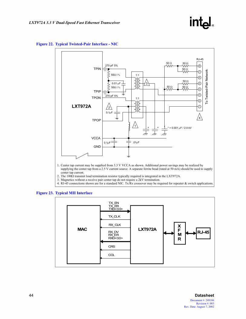
LXT972A 3.3 V Dual-Speed Fast Ethernet Transceiver
Figure 22. Typical Twisted-Pair Interface - NIC
1. Center tap current may be supplied from 3.3 V VCCA as shown. Additional power savings may be realized by supplying the center tap from a 2.5 V current source. A separate ferrite bead (rated at 50 mA) should be used to supply center tap current.
2. The 100Ω transmit load termination resistor typically required is integrated in the LXT972A.3. Magnetics without a receive pair center tap do not require a 2kV termination.4. RJ-45 connections shown are for a standard NIC. Tx/Rx crossover may be required for repeater & switch applications.
Figure 23. Typical MII Interface
TPIP
TPIN
* = 0.001 µF / 2.0 kV
To T
wis
ted-
Pair
Net
wor
k
1:1
LXT972A
1:1
1
TPOP
TPON
VCCA
GND0.1µF .01µF
2
270 pF 5%
270 pF 5%
0.01 µF
50Ω 1%
50Ω 1%
* *
3
6
3
8
7
5
4
1
2
50 Ω
50 Ω 50 ΩRJ-45
50 Ω50 Ω
50 Ω
4
0.1µF
MAC
TX_ENTX_ERTXD<3:0>
TX_CLK
RX_DVRX_ERRXD<3:0>
CRS
COL
LXT972A X
RJ-45 F M R
RX_CLK
44 DatasheetDocument #: 249186
Revision #: 003Rev. Date: August 7, 2002

LXT972A 3.3 V Dual-Speed Fast Ethernet Transceiver
5.0 Test Specifications
Note: Table 17 through Table 36 and Figure 24 through Figure 35 represent the target specifications of the LXT972A. These specifications are guaranteed by test except where noted “by design.” Minimum and maximum values listed in Table 19 through Table 36 apply over the recommended operating conditions specified in Table 18.
5.1 Electrical Parameters
Table 17. Absolute Maximum Ratings
Parameter Sym Min Max Units
Supply voltage VCC -0.3 4.0 V
Operating temperature TOPA -15 +85 ºC
Storage temperature TST -65 +150 ºC
Caution: Exceeding these values may cause permanent damage. Functional operation under these conditions is not implied. Exposure to maximum rating conditions for extended periods may affect device reliability.
Table 18. Operating Conditions
Parameter Sym Min Typ1 Max Units
Recommended operating temperature
LXT972A_C (Commercial) TOPA 0 – 70 ºC
Recommended supply voltage2Analog & Digital Vcca, Vccd 3.14 3.3 3.45 V
I/O Vccio 2.35 – 3.45 V
VCC current
100BASE-TX ICC – 92 110 mA
10BASE-T ICC – 66 82 mA
Hard Power Down ICC – – 1 mA
Soft Power Down Icc – 51 –
Auto-Negotiation ICC – 90 110 mA
1. Typical values are at 25 °C and are for design aid only; not guaranteed and not subject to production testing.2. Voltages with respect to ground unless otherwise specified.
Datasheet 45Document #: 249186Revision #: 003Rev. Date: August 7, 2002

LXT972A 3.3 V Dual-Speed Fast Ethernet Transceiver
Table 19. Digital I/O Characteristics1
Parameter Symbol Min Typ2 Max Units Test Conditions
Input Low voltage VIL – – 0.8 V –
Input High voltage VIH 2.0 – – V –
Input current II -10 – 10 µA 0.0 < VI < VCC
Output Low voltage VOL – – 0.4 V IOL = 4 mA
Output High voltage VOH 2.4 – – V IOH = -4 mA
1. Applies to all pins except MII, LED and XI/XO pins. Refer to Table 20 for MII I/O Characteristics, Table 21 for XI/XO and Table 22 for LED Characteristics.
2. Typical values are at 25 °C and are for design aid only; not guaranteed and not subject to production testing.
Table 20. Digital I/O Characteristics - MII Pins
Parameter Symbol Min Typ1 Max Units Test Conditions
Input Low voltage VIL – – 0.8 V –
Input High voltage VIH 2.0 – – V –
Input current II -10 – 10 µA 0.0 < VI < VCCIO
Output Low voltage VOL – – 0.4 V IOL = 4 mA
Output High voltageVOH 2.2 – – V IOH = -4 mA, VCCIO = 3.3 V
VOH 2.0 – – V IOH = -4 mA, VCCIO = 2.5 V
Driver output resistance(Line driver output enabled)
RO2 – 100 – Ω VCCIO = 2.5 V
RO2 – 100 – Ω VCCIO = 3.3 V
1. Typical values are at 25 °C and are for design aid only; not guaranteed and not subject to production testing.2. Parameter is guaranteed by design; not subject to production testing.
Table 21. I/O Characteristics - REFCLK/XI and XO Pins
Parameter Sym Min Typ1 Max Units Test Conditions
Input Low Voltage VIL – – 0.8 V –
Input High Voltage VIH 2.0 – – V –
Input Clock Frequency Tolerance2 ∆f – – ±100 ppm –
Input Clock Duty Cycle2 Tdc 35 – 65 % –
Input Capacitance CIN – 3.0 – pF –
1. Typical values are at 25 °C and are for design aid only; not guaranteed and not subject to production testing.2. Parameter is guaranteed by design; not subject to production testing.
Table 22. I/O Characteristics - LED/CFG Pins
Parameter Symbol Min Typ Max Units Test Conditions
Input Low Voltage VIL – – 0.8 V –
Input High Voltage VIH 2.0 – – V –
46 DatasheetDocument #: 249186
Revision #: 003Rev. Date: August 7, 2002

LXT972A 3.3 V Dual-Speed Fast Ethernet Transceiver
Input Current II -10 – 10 µA 0 < VI < VCCIO
Output Low Voltage VOL – – 0.4 V IOL = 10 mA
Output High Voltage VOH 2.0 – – V IOH = -10 mA
Table 23. 100BASE-TX Transceiver Characteristics
Parameter Sym Min Typ1 Max Units Test Conditions
Peak differential output voltage VP 0.95 – 1.05 V Note 2
Signal amplitude symmetry Vss 98 – 102 % Note 2
Signal rise/fall time TRF 3.0 – 5.0 ns Note 2
Rise/fall time symmetry TRFS – – 0.5 ns Note 2
Duty cycle distortion DCD 35 50 65 %Offset from 16ns pulse width at 50% of pulse peak
Overshoot/Undershoot VOS – – 5 % –
Jitter (measured differentially) – – – 1.4 ns –
1. Typical values are at 25 °C and are for design aid only; not guaranteed and not subject to production testing.2. Measured at the line side of the transformer, line replaced by 100Ω(+/-1%) resistor.
Table 24. 10BASE-T Transceiver Characteristics
Parameter Sym Min Typ Max Units Test Conditions
Transmitter
Peak differential output voltage VOP 2.2 2.5 2.8 V
With transformer, line replaced by 100 Ω resistor
Transition timing jitter added by the MAU and PLS sections - 0 2 11 ns
After line model specified by IEEE 802.3 for 10BASE-T MAU
Receiver
Receive Input Impedance ZIN - - 22 kΩ
Differential Squelch Threshold VDS 300 420 585 mV
Table 25. 10BASE-T Link Integrity Timing Characteristics
Parameter Sym Min Typ Max Units Test Conditions
Time Link Loss Receive TLL 50 – 150 ms –
Link Pulse TLP 2 – 7 Link Pulses –
Link Min Receive Timer TLR MIN 2 – 7 ms –
1. Typical values are at 25 °C and are for design aid only; not guaranteed and not subject to production testing.
Table 22. I/O Characteristics - LED/CFG Pins (Continued)
Parameter Symbol Min Typ Max Units Test Conditions
Datasheet 47Document #: 249186Revision #: 003Rev. Date: August 7, 2002
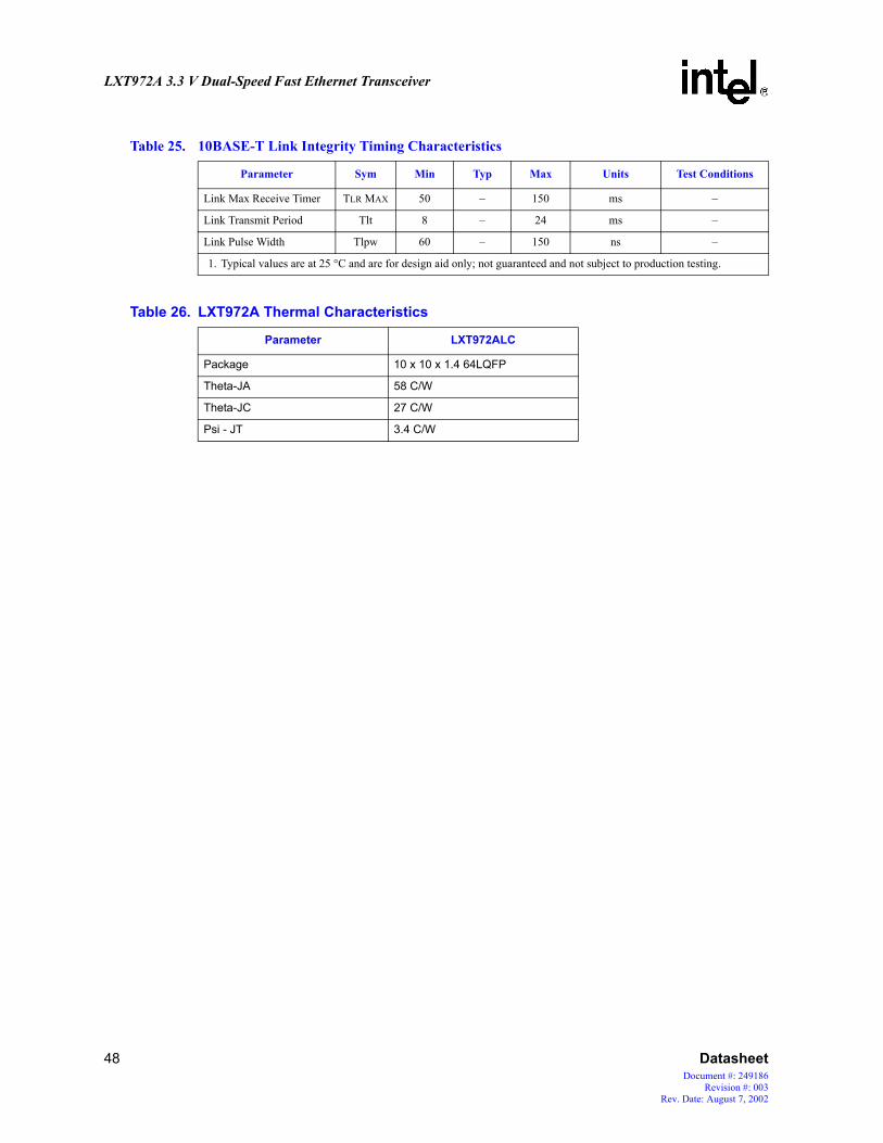
LXT972A 3.3 V Dual-Speed Fast Ethernet Transceiver
Link Max Receive Timer TLR MAX 50 – 150 ms –
Link Transmit Period Tlt 8 – 24 ms –
Link Pulse Width Tlpw 60 – 150 ns –
Table 26. LXT972A Thermal Characteristics
Parameter LXT972ALC
Package 10 x 10 x 1.4 64LQFP
Theta-JA 58 C/W
Theta-JC 27 C/W
Psi - JT 3.4 C/W
Table 25. 10BASE-T Link Integrity Timing Characteristics
Parameter Sym Min Typ Max Units Test Conditions
1. Typical values are at 25 °C and are for design aid only; not guaranteed and not subject to production testing.
48 DatasheetDocument #: 249186
Revision #: 003Rev. Date: August 7, 2002

LXT972A 3.3 V Dual-Speed Fast Ethernet Transceiver
5.2 Timing Diagrams
Figure 24. 100BASE-TX Receive Timing - 4B Mode
Table 27. 100BASE-TX Receive Timing Parameters - 4B Mode
Parameter Sym Min Typ1 Max Units2 Test Conditions
RXD<3:0>, RX_DV, RX_ER setup to RX_CLK High t1 10 – – ns –
RXD<3:0>, RX_DV, RX_ER hold from RX_CLK High t2 10 – – ns –
CRS asserted to RXD<3:0>, RX_DV t3 3 – 5 BT –
Receive start of “J” to CRS asserted t4 12 – 16 BT –
Receive start of “T” to CRS de-asserted t5 10 – 17 BT –
Receive start of “J” to COL asserted t6 16 – 22 BT –
Receive start of “T” to COL de-asserted t7 17 – 20 BT –
1. Typical values are at 25 °C and are for design aid only; not guaranteed and not subject to production testing.2. BT is the duration of one bit as transferred to and from the MAC and is the reciprocal of the bit rate. 100BASE-T bit
time = 10-8 s or 10 ns.
t4 t5
t3
t6 t7
0 ns 250 ns
CRS
RX_DV
RXD<3:0>
RX_CLK
COL
t1t2
TPI
Datasheet 49Document #: 249186Revision #: 003Rev. Date: August 7, 2002
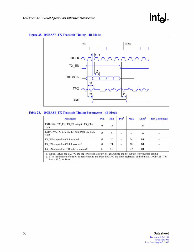
LXT972A 3.3 V Dual-Speed Fast Ethernet Transceiver
Figure 25. 100BASE-TX Transmit Timing - 4B Mode
Table 28. 100BASE-TX Transmit Timing Parameters - 4B Mode
Parameter Sym Min Typ1 Max Units2 Test Conditions
TXD<3:0>, TX_EN, TX_ER setup to TX_CLK High t1 12 – – ns –
TXD<3:0>, TX_EN, TX_ER hold from TX_CLK High t2 0 – – ns –
TX_EN sampled to CRS asserted t3 20 – 24 BT –
TX_EN sampled to CRS de-asserted t4 24 – 28 BT –
TX_EN sampled to TPO out (Tx latency) t5 5.3 – 5.7 BT –
1. Typical values are at 25 °C and are for design aid only; not guaranteed and not subject to production testing.2. BT is the duration of one bit as transferred to and from the MAC and is the reciprocal of the bit rate. 100BASE-T bit
time = 10-8 s or 10 ns.
t1
t2
t5
t3 t4
0ns 250ns
TXCLK
TX_EN
TXD<3:0>
TPO
CRS
50 DatasheetDocument #: 249186
Revision #: 003Rev. Date: August 7, 2002

LXT972A 3.3 V Dual-Speed Fast Ethernet Transceiver
Figure 26. 10BASE-T Receive Timing
Table 29. 10BASE-T Receive Timing Parameters
Parameter Sym Min Typ1 Max Units2 Test Conditions
RXD, RX_DV, RX_ER Setup to RX_CLK High t1 10 – – ns –
RXD, RX_DV, RX_ER Hold from RX_CLK High t2 10 – – ns –
TPIP/N in to RXD out (Rx latency) t3 4.2 – 6.6 BT –
CRS asserted to RXD, RX_DV, RX_ER asserted t4 5 – 32 BT –
RXD, RX_DV, RX_ER de-asserted to CRS de-asserted t5 0.3 – 0.5 BT –
TPI in to CRS asserted t6 2 – 28 BT –
TPI quiet to CRS de-asserted t7 6 – 10 BT –
TPI in to COL asserted t8 1 – 31 BT –
TPI quiet to COL de-asserted t9 5 – 10 BT –
1. Typical values are at 25 °C and are for design aid only; not guaranteed and not subject to production testing.2. BT is the duration of one bit as transferred to and from the MAC and is the reciprocal of the bit rate. 10BASE-T bit
time = 10-7 s or 100 ns.
RX_CLK
RXD,RX_DV,RX_ER
CRS
TPI
t3
t4
t2
t6
t1
t7
t5
COLt8
t9
Datasheet 51Document #: 249186Revision #: 003Rev. Date: August 7, 2002
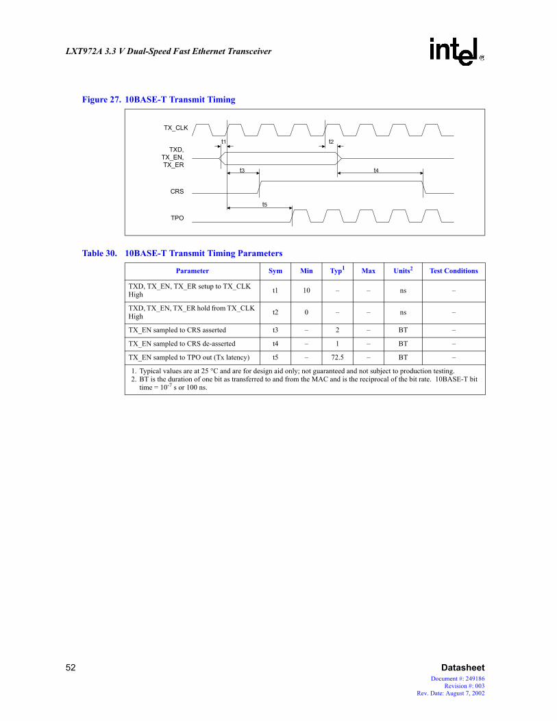
LXT972A 3.3 V Dual-Speed Fast Ethernet Transceiver
Figure 27. 10BASE-T Transmit Timing
Table 30. 10BASE-T Transmit Timing Parameters
Parameter Sym Min Typ1 Max Units2 Test Conditions
TXD, TX_EN, TX_ER setup to TX_CLK High t1 10 – – ns –
TXD, TX_EN, TX_ER hold from TX_CLK High t2 0 – – ns –
TX_EN sampled to CRS asserted t3 – 2 – BT –
TX_EN sampled to CRS de-asserted t4 – 1 – BT –
TX_EN sampled to TPO out (Tx latency) t5 – 72.5 – BT –
1. Typical values are at 25 °C and are for design aid only; not guaranteed and not subject to production testing.2. BT is the duration of one bit as transferred to and from the MAC and is the reciprocal of the bit rate. 10BASE-T bit
time = 10-7 s or 100 ns.
TX_CLK
TXD,TX_EN,TX_ER
CRS
TPO
t1
t3 t4
t5
t2
52 DatasheetDocument #: 249186
Revision #: 003Rev. Date: August 7, 2002

LXT972A 3.3 V Dual-Speed Fast Ethernet Transceiver
Figure 28. 10BASE-T Jabber and Unjabber Timing
Table 31. 10BASE-T Jabber and Unjabber Timing Parameters
Parameter Sym Min Typ1 Max Units Test Conditions
Maximum transmit time t1 20 – 150 ms –
Unjab time t2 250 – 750 ms –
1. Typical values are at 25 °C and are for design aid only; not guaranteed and not subject to production testing.
Figure 29. 10BASE-T SQE (Heartbeat) Timing
Table 32. 10BASE-T SQE Timing Parameters
Parameter Sym Min Typ1 Max Units Test Conditions
COL (SQE) Delay after TX_EN off t1 0.65 – 1.6 us –
COL (SQE) Pulse duration t2 0.5 – 1.5 us –
1. Typical values are at 25 °C and are for design aid only; not guaranteed and not subject to production testing.
TXD
COL
t1
t2
TX_EN
TX_CLK
TX_EN
t1t2COL
Datasheet 53Document #: 249186Revision #: 003Rev. Date: August 7, 2002

LXT972A 3.3 V Dual-Speed Fast Ethernet Transceiver
Figure 30. Auto Negotiation and Fast Link Pulse Timing
Figure 31. Fast Link Pulse Timing
Table 33. Auto Negotiation and Fast Link Pulse Timing Parameters
Parameter Sym Min Typ1 Max Units Test Conditions
Clock/Data pulse width t1 – 100 – ns –
Clock pulse to Data pulse t2 55.5 – 63.8 µs –
Clock pulse to Clock pulse t3 123 – 127 µs –
FLP burst width t4 – 2 – ms –
FLP burst to FLP burst t5 8 12 24 ms –
Clock/Data pulses per burst – 17 – 33 ea –
1. Typical values are at 25 °C and are for design aid only; not guaranteed and not subject to production testing.
TPOt1 t1
t2t3
Clock Pulse Data Pulse Clock Pulse
TPO
t4t5
FLP Burst FLP Burst
54 DatasheetDocument #: 249186
Revision #: 003Rev. Date: August 7, 2002

LXT972A 3.3 V Dual-Speed Fast Ethernet Transceiver
Figure 32. MDIO Input Timing
Figure 33. MDIO Output Timing
Table 34. MDIO Timing Parameters
Parameter Sym Min Typ1 Max Units Test Conditions
MDIO setup before MDC, sourced by STA t1 10 – – ns –
MDIO hold after MDC, sourced by STA t2 5 – – ns –
MDC to MDIO output delay, source by PHY t3 – – 150 ns –
MDC period t4 125 – – ns MDC = 8 MHz
1. Typical values are at 25° C and are for design aid only; not guaranteed and not subject to production testing.
t1
MDC
MDIO
t2
t3
MDC
MDIO
t4
Datasheet 55Document #: 249186Revision #: 003Rev. Date: August 7, 2002

LXT972A 3.3 V Dual-Speed Fast Ethernet Transceiver
Figure 34. Power-Up Timing
Table 35. Power-Up Timing Parameters
Parameter Sym Min Typ1 Max Units Test Conditions
Voltage threshold v1 – 2.9 – V –
Power Up delay2 t1 – – 300 µs –
1. Typical values are at 25° C and are for design aid only; not guaranteed and not subject to production testing. 2. Power Up Delay is specified as a maximum value because it refers to the PHY's guaranteed performance - the PHY
comes out of reset after a delay of No MORE Than 300 µs. System designers should consider this as a minimum value - After threshold v1 is reached, the MAC should delay No LESS Than 300 µs before accessing the MDIO port.
Figure 35. RESET Pulse Width and Recovery Timing
Table 36. RESET Pulse Width and Recovery Timing Parameters
Parameter Sym Min Typ1 Max Units Test Conditions
RESET pulse width t1 10 – – ns –
RESET recovery delay2 t2 – – 300 µs –
1. Typical values are at 25° C and are for design aid only; not guaranteed and not subject to production testing. 2. Reset Recovery Delay is specified as a maximum value because it refers to the PHY's guaranteed performance - the
PHY comes out of reset after a delay of No MORE Than 300 µs. System designers should consider this as a minimum value - After de-asserting RESET*, the MAC should delay No LESS Than 300 µs before accessing the MDIO port.
t1VCCMDIO,etc
v1
t2
RESET
MDIO,etc
t1
56 DatasheetDocument #: 249186
Revision #: 003Rev. Date: August 7, 2002

LXT972A 3.3 V Dual-Speed Fast Ethernet Transceiver
6.0 Register Definitions
The LXT972A register set includes multiple 16-bit registers. Refer to Table 37 for a complete register listing.
• Base registers (0 through 8) are defined in accordance with the “Reconciliation Sublayer and Media Independent Interface” and “Physical Layer Link Signaling for 10/100 Mbps Auto-Negotiation” sections of the IEEE 802.3 standard.
• Additional registers are defined in accordance with the IEEE 802.3 standard for adding unique chip functions.
Table 37. Register Set
Address Register Name Bit Assignments
0 Control Register Refer to Table 39 on page 60
1 Status Register #1 Refer to Table 40 on page 61
2 PHY Identification Register 1 Refer to Table 41 on page 62
3 PHY Identification Register 2 Refer to Table 42 on page 62
4 Auto-Negotiation Advertisement Register Refer to Table 43 on page 63
5 Auto-Negotiation Link Partner Base Page Ability Register Refer to Table 44 on page 64
6 Auto-Negotiation Expansion Register Refer to Table 45 on page 65
7 Auto-Negotiation Next Page Transmit Register Refer to Table 46 on page 65
8 Auto-Negotiation Link Partner Received Next Page Register Refer to Table 47 on page 66
9 1000BASE-T/100BASE-T2 Control Register Not Implemented
10 1000BASE-T/100BASE-T2 Status Register Not Implemented
15 Extended Status Register Not Implemented
16 Port Configuration Register Refer to Table 48 on page 66
17 Status Register #2 Refer to Table 49 on page 67
18 Interrupt Enable Register Refer to Table 50 on page 68
19 Interrupt Status Register Refer to Table 51 on page 68
20 LED Configuration Register Refer to Table 52 on page 70
21-25 Reserved –
26
27-30 Transmit Control Register Refer to Table 54 on page 72
Datasheet 57Document #: 249186Revision #: 003Rev. Date: August 7, 2002

LXT972A 3.3 V Dual-Speed Fast Ethernet Transceiver
Add
rB
2B
1B
0
Res
erve
d0
ityLi
nk S
tatu
sJa
bber
D
etec
tEx
tend
ed
Cap
abili
ty1
21
02
MFR
Rev
No
3
IEEE
Sel
ecto
r Fie
ld4
IEEE
Sel
ecto
r Fie
ld5
k er
age
e
Nex
t Pag
e A
ble
Page
R
ecei
ved
Link
Pa
rtner
A
/N A
ble
6 7 8
Res
erve
dA
ltern
ate
Nex
t Pag
eR
eser
ved
16
Tabl
e 38
. R
egis
ter
Bit
Map
Reg
Titl
eB
it Fi
elds
B15
B14
B13
B12
B11
B10
B9
B8
B7
B6
B5
B4
B3
Con
trol
Reg
iste
r
Con
trol
Res
etLo
opba
ckSp
eed
Sele
ctA
/N
Enab
lePo
wer
D
own
Isol
ate
Re-
star
t A/
ND
uple
x M
ode
CO
L Te
stSp
eed
Sele
ct
Stat
us R
egis
ter
Stat
us10
0Bas
e-T4
100B
ase-
X
Full
Dup
lex
100B
ase-
X
Hal
f D
uple
x
10 M
bps
Full
Dup
lex
10 M
bps
Hal
f D
uple
x
100B
ase-
T2 F
ull
Dup
lex
100B
ase-
T2 H
alf
Dup
lex
Exte
nded
St
atus
Res
erve
dM
F Pr
eam
ble
Supp
ress
A/N
C
ompl
ete
Rem
ote
Faul
tA
/NA
bil
PHY
ID R
egis
ters
PHY
ID 1
1514
1312
1110
98
76
54
3
PHY
ID2
PHY
ID N
oM
FR M
odel
No
Aut
o-N
egot
iatio
n A
dver
tisem
ent R
egis
ter
A/N
Adv
ertis
eN
ext P
age
Res
erve
dR
emot
e Fa
ult
Res
erve
dA
sym
m
Paus
ePa
use
100B
ase-
T410
0Bas
e-TX
Ful
l D
uple
x10
0Bas
e-TX
10B
ase-
T Fu
ll D
uple
x10
Bas
e-T
Aut
o-N
egot
iatio
n L
ink
Part
ner
Bas
e Pa
ge A
bilit
y R
egis
ter
A/N
Lin
k A
bilit
yN
ext P
age
Ack
Rem
ote
Faul
tR
eser
ved
Asy
mm
Pa
use
Paus
e10
0Bas
e-T4
100B
ase-
TX F
ull
Dup
lex
100B
ase-
TX10
Bas
e-T
Full
Dup
lex
10B
ase-
T
Aut
o-N
egot
iatio
n E
xpan
sion
Reg
iste
r
A/N
Exp
ansi
onR
eser
ved
Bas
e Pa
gePa
ralle
l D
etec
t Fa
ult
Lin
Partn
Nex
t P Abl
Aut
o-N
egot
iatio
n N
ext P
age
Tran
smit
Reg
iste
r
A/N
Nex
t Pag
e T
xmit
Nex
t Pag
eR
eser
ved
Mes
sage
Pa
geA
ck 2
Togg
leM
essa
ge /
Unf
orm
atte
d C
ode
Fiel
d
Aut
o-N
egot
iatio
n L
ink
Part
ner
Nex
t Pag
e R
ecei
ve R
egis
ter
A/N
Lin
k N
ext
Page
Nex
t Pag
eA
ckM
essa
ge
Page
Ack
2To
ggle
Mes
sage
/ U
nfor
mat
ted
Cod
e Fi
eld
Con
figur
atio
n R
egis
ter
Port
Con
figR
eser
ved
Forc
e Lin
k Pa
ssTx
mit
Dis
able
Byp
ass
Scra
mbl
er(1
00TX
)R
eser
ved)
Jabb
er(1
0T)
SQE
(10T
)
TP
Loop
back
(10T
)C
RS
Sele
ct
(10T
)R
eser
ved
PRE_
ENR
eser
ved
58 DatasheetDocument #: 249186
Revision #: 003Rev. Date: August 7, 2002

LXT972A 3.3 V Dual-Speed Fast Ethernet Transceiver
rR
eser
ved
Res
erve
d17
ved
Res
erve
dIn
terr
upt
Enab
leTe
st
Inte
rrup
t18
ved
MD
In
terr
upt
Res
erve
dR
eser
ved
19
LED
Fre
qPu
lse
Stre
tch
Res
erve
d20 26 30Add
rB
2B
1B
0
Stat
us R
egis
ter
#2
Stat
us R
egis
ter
#2R
eser
ved
10/1
00
Mod
eTr
ansm
it St
atus
Rec
eive
St
atus
Col
lisio
n St
atus
Link
Dup
lex
Mod
eA
uto-
Neg
Aut
o-N
eg
Com
plet
eR
eser
ved
Pola
rity
Paus
eEr
ro
Inte
rrup
t Ena
ble
Reg
iste
r
Inte
rrup
t E
nabl
eR
eser
ved
Res
erve
dA
uto-
Neg
M
ask
Spee
d M
ask
Dup
lex
Mas
kLi
nk M
ask
Res
er
Inte
rrup
t Sta
tus R
egis
ter
Inte
rrup
t St
atus
Res
erve
dR
eser
ved
Aut
o-N
eg
Don
eSp
eed
Cha
nge
Dup
lex
Cha
nge
Link
C
hang
eR
eser
LE
D C
onfig
urat
ion
Reg
iste
r
LE
D C
onfig
LED
1LE
D2
LED
3
Dig
ital C
onfig
Reg
iste
r
Dig
ital C
onfig
Res
erve
dSt
rong
D
igita
l Pa
cs
Res
erve
dSh
ow
Sym
bol
Erro
r
Res
erve
d
Tran
smit
Con
trol
Reg
iste
r
Tran
s. C
ontr
olR
eser
ved
Tran
smit
Low
Pw
rPo
rt R
ise
Tim
e C
ontro
lR
eser
ved
Tabl
e 38
. R
egis
ter
Bit
Map
(Con
tinue
d)
Reg
Titl
eB
it Fi
elds
B15
B14
B13
B12
B11
B10
B9
B8
B7
B6
B5
B4
B3
Datasheet 59Document #: 249186Revision #: 003Rev. Date: August 7, 2002

LXT972A 3.3 V Dual-Speed Fast Ethernet Transceiver
Table 39. Control Register (Address 0)
Bit Name Description Type 1 Default
0.15 Reset1 = PHY reset0 = Normal operation
R/WSC
0
0.14 Loopback 1 = Enable loopback mode0 = Disable loopback mode R/W 0
0.13 Speed Selection
0.6 0.13 Speed Selected
R/W Note 2 1 1 0 0
1010
Reserved1000 Mbps (not supported)100 Mbps10 Mbps
0.12 Auto-Negotiation Enable
1 = Enable Auto-Negotiation Process0 = Disable Auto-Negotiation Process R/W Note 2
0.11 Power-Down 1 = Power-down0 = Normal operation R/W 0
0.10 Isolate 1 = Electrically isolate PHY from MII0 = Normal operation R/W 0
0.9Restart Auto-Negotiation
1 = Restart Auto-Negotiation Process0 = Normal operation
R/WSC
0
0.8 Duplex Mode 1 = Full Duplex0 = Half Duplex R/W Note 2
0.7 Collision Test 1 = Enable COL signal test0 = Disable COL signal test R/W 0
0.6 Speed Selection
0.6 0.13 Speed Selected
R/W 0 1 1 0 0
1010
Reserved1000 Mbps (not supported)100 Mbps10 Mbps
0.5:0 Reserved Write as 0, ignore on Read R/W 00000
1. R/W = Read/WriteRO = Read OnlySC = Self Clearing
2. Default value of bits 0.12, 0.13 and 0.8 are determined by the LED/CFG pins (refer to Table 9 on page 25).
Table 40. MII Status Register #1 (Address 1)
Bit Name Description Type 1 Default
1.15100BASE-T4Not Supported
1 = PHY able to perform 100BASE-T40 = PHY not able to perform 100BASE-T4 RO 0
1.14 100BASE-X Full-Duplex
1 = PHY able to perform full-duplex 100BASE-X0 = PHY not able to perform full-duplex 100BASE-X RO 1
1.13 100BASE-X Half-Duplex
1 = PHY able to perform half-duplex 100BASE-X0 = PHY not able to perform half-duplex 100BASE-X RO 1
1. RO = Read OnlyLL = Latching LowLH = Latching High
60 DatasheetDocument #: 249186
Revision #: 003Rev. Date: August 7, 2002

LXT972A 3.3 V Dual-Speed Fast Ethernet Transceiver
1.12 10 Mbps Full-Duplex1 = PHY able to operate at 10 Mbps in full-duplex mode0 = PHY not able to operate at 10 Mbps full-duplex mode
RO 1
1.11 10 Mbps Half-Duplex 1 = PHY able to operate at 10 Mbps in half-duplex mode0 = PHY not able to operate at 10 Mbps in half-duplex RO 1
1.10100BASE-T2 Full-DuplexNot Supported
1 = PHY able to perform full-duplex 100BASE-T20 = PHY not able to perform full-duplex 100BASE-T2 RO 0
1.9100BASE-T2 Half-DuplexNot Supported
1 = PHY able to perform half duplex 100BASE-T20 = PHY not able to perform half-duplex 100BASE-T2 RO 0
1.8 Extended Status 1 = Extended status information in register 150 = No extended status information in register 15 RO 0
1.7 Reserved 1 = ignore when read RO 0
1.6 MF Preamble Suppression
1 = PHY accepts management frames with preamble suppressed0 = PHY will not accept management frames with preamble suppressed
RO 0
1.5 Auto-Negotiation Complete
1 = Auto-negotiation complete0 = Auto-negotiation not complete RO 0
1.4 Remote Fault 1 = Remote fault condition detected0 = No remote fault condition detected RO/LH 0
1.3 Auto-Negotiation Ability
1 = PHY is able to perform Auto-Negotiation0 = PHY is not able to perform Auto-Negotiation RO 1
1.2 Link Status 1 = Link is up0 = Link is down RO/LL 0
1.1 Jabber Detect 1 = Jabber condition detected0 = Jabber condition not detected RO/LH 0
1.0 Extended Capability 1 = Extended register capabilities0 = Basic register capabilities RO 1
Table 41. PHY Identification Register 1 (Address 2)
Bit Name Description Type 1 Default
2.15:0 PHY ID Number The PHY identifier composed of bits 3 through 18 of the OUI. RO 0013 hex
1. RO = Read Only
Table 40. MII Status Register #1 (Address 1)
Bit Name Description Type 1 Default
1. RO = Read OnlyLL = Latching LowLH = Latching High
Datasheet 61Document #: 249186Revision #: 003Rev. Date: August 7, 2002

LXT972A 3.3 V Dual-Speed Fast Ethernet Transceiver
Table 42. PHY Identification Register 2 (Address 3)
Bit Name Description Type 1 Default
3.15:10 PHY ID number The PHY identifier composed of bits 19 through 24 of the OUI. RO 011110
3.9:4 Manufacturer’s model number
6 bits containing manufacturer’s part number. RO 001110
3.3:0 Manufacturer’s revision number
4 bits containing manufacturer’s revision number. RO
xxxx(See LXT971A/972A Specification Update)
1. RO = Read Only
Figure 36. PHY Identifier Bit Mapping
0 0 0 0 0 000 0 0 0 0 0 1 0 0 1 1 0 1 1 1 1 0 0 0 1 1 1 0 0 0
a b c r s x
15015 10 9 4 3 00 0
The Intel OUI is 00207B hex
PHY ID Register #1 (address 2) = 0013 PHY ID Register #2 (Address 3)
Manufacturer’s Model Number
RevisionNumber
Organizationally Unique Identifier
00 20 7B5 0 3 0
62 DatasheetDocument #: 249186
Revision #: 003Rev. Date: August 7, 2002
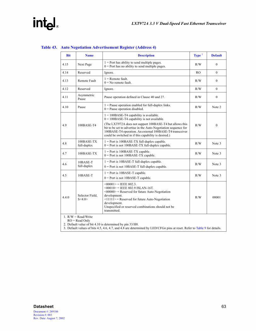
LXT972A 3.3 V Dual-Speed Fast Ethernet Transceiver
Table 43. Auto Negotiation Advertisement Register (Address 4)
Bit Name Description Type 1 Default
4.15 Next Page 1 = Port has ability to send multiple pages.0 = Port has no ability to send multiple pages. R/W 0
4.14 Reserved Ignore. RO 0
4.13 Remote Fault 1 = Remote fault.0 = No remote fault. R/W 0
4.12 Reserved Ignore. R/W 0
4.11 Asymmetric Pause Pause operation defined in Clause 40 and 27. R/W 0
4.10 Pause 1 = Pause operation enabled for full-duplex links.0 = Pause operation disabled. R/W Note 2
4.9 100BASE-T4
1 = 100BASE-T4 capability is available.0 = 100BASE-T4 capability is not available.(The LXT972A does not support 100BASE-T4 but allows this bit to be set to advertise in the Auto-Negotiation sequence for 100BASE-T4 operation. An external 100BASE-T4 transceiver could be switched in if this capability is desired.)
R/W 0
4.8 100BASE-TXfull-duplex
1 = Port is 100BASE-TX full-duplex capable.0 = Port is not 100BASE-TX full-duplex capable. R/W Note 3
4.7 100BASE-TX 1 = Port is 100BASE-TX capable.0 = Port is not 100BASE-TX capable. R/W Note 3
4.6 10BASE-Tfull-duplex
1 = Port is 10BASE-T full-duplex capable.0 = Port is not 10BASE-T full-duplex capable.
R/W Note 3
4.5 10BASE-T1 = Port is 10BASE-T capable.0 = Port is not 10BASE-T capable.
R/W Note 3
4.4:0 Selector Field,S<4:0>
<00001> = IEEE 802.3.<00010> = IEEE 802.9 ISLAN-16T.<00000> = Reserved for future Auto-Negotiation development.<11111> = Reserved for future Auto-Negotiation development.Unspecified or reserved combinations should not be transmitted.
R/W 00001
1. R/W = Read/WriteRO = Read Only
2. Default value of bit 4.10 is determined by pin 33/H8.3. Default values of bits 4.5, 4.6, 4.7, and 4.8 are determined by LED/CFGn pins at reset. Refer to Table 9 for details.
Datasheet 63Document #: 249186Revision #: 003Rev. Date: August 7, 2002

LXT972A 3.3 V Dual-Speed Fast Ethernet Transceiver
Table 44. Auto Negotiation Link Partner Base Page Ability Register (Address 5)
Bit Name Description Type 1 Default
5.15 Next Page 1 = Link Partner has ability to send multiple pages.0 = Link Partner has no ability to send multiple pages. RO N/A
5.14 Acknowledge
1 = Link Partner has received Link Code Word from LXT972A.0 = Link Partner has not received Link Code Word from the LXT972A.
RO N/A
5.13 Remote Fault 1 = Remote fault.0 = No remote fault. RO N/A
5.12 Reserved Ignore. RO N/A
5.11 Asymmetric Pause
Pause operation defined in Clause 40 and 27.1 = Link Partner is Pause capable.0 = Link Partner is not Pause capable.
RO N/A
5.10 Pause 1 = Link Partner is Pause capable.0 = Link Partner is not Pause capable. RO N/A
5.9 100BASE-T4 1 = Link Partner is 100BASE-T4 capable.0 = Link Partner is not 100BASE-T4 capable. RO N/A
5.8 100BASE-TXfull-duplex
1 = Link Partner is 100BASE-TX full-duplex capable.0 = Link Partner is not 100BASE-TX full-duplex capable. RO N/A
5.7 100BASE-TX 1 = Link Partner is 100BASE-TX capable.0 = Link Partner is not 100BASE-TX capable. RO N/A
5.610BASE-Tfull-duplex
1 = Link Partner is 10BASE-T full-duplex capable.0 = Link Partner is not 10BASE-T full-duplex capable. RO N/A
5.5 10BASE-T 1 = Link Partner is 10BASE-T capable.0 = Link Partner is not 10BASE-T capable. RO N/A
5.4:0 Selector FieldS<4:0>
<00001> = IEEE 802.3.<00010> = IEEE 802.9 ISLAN-16T.<00000> = Reserved for future Auto-Negotiation development.<11111> = Reserved for future Auto-Negotiation development.Unspecified or reserved combinations shall not be transmitted.
RO N/A
1. RO = Read Only
64 DatasheetDocument #: 249186
Revision #: 003Rev. Date: August 7, 2002

LXT972A 3.3 V Dual-Speed Fast Ethernet Transceiver
Table 45. Auto Negotiation Expansion (Address 6)
Bit Name Description Type 1 Default
6.15:6 Reserved Ignore on read. RO 0
6.5 Base Page
This bit indicates the status of the Auto-Negotiation variable, base page. It flags synchronization with the Auto-Negotiation state diagram allowing detection of interrupted links. This bit is only used if bit 16.1 (Alternate NP feature) is set.1 = basepage = true0 = basepage = false
RO/LH 0
6.4 Parallel Detection Fault
1 = Parallel detection fault has occurred.0 = Parallel detection fault has not occurred.
RO/LH
0
6.3 Link Partner Next Page Able
1 = Link partner is next page able.0 = Link partner is not next page able. RO 0
6.2 Next Page Able 1 = Local device is next page able.0 = Local device is not next page able. RO 1
6.1 Page Received
1 = Indicates that a new page has been received and the received code word has been loaded into register 5 (base pages) or register 8 (next pages) as specified in clause 28 of 802.3. This bit is cleared on read. If bit 16.1 is set, the Page Received bit is also cleared when mr_page_rx = false or transmit_disable = true.
ROLH 0
6.0 Link Partner A/N Able
1 = Link partner is auto-negotiation able.0 = Link partner is not auto-negotiation able. RO 0
1. RO = Read Only LH = Latching High
Table 46. Auto Negotiation Next Page Transmit Register (Address 7)
Bit Name Description Type 1 Default
7.15Next Page(NP)
1 = Additional next pages follow0 = Last page
R/W 0
7.14 Reserved Write as 0, ignore on read RO 0
7.13Message Page(MP)
1 = Message page0 = Unformatted page
R/W 1
7.12Acknowledge 2(ACK2)
1 = Complies with message0 = Can not comply with message
R/W 0
7.11Toggle(T)
1 = Previous value of the transmitted Link Code Word equalled logic zero0 = Previous value of the transmitted Link Code Word equalled logic one
R/W 0
7.10:0 Message/Unformatted Code Field R/W 000000000
01
1. RO = Read Only. R/W = Read/Write
Datasheet 65Document #: 249186Revision #: 003Rev. Date: August 7, 2002

LXT972A 3.3 V Dual-Speed Fast Ethernet Transceiver
Table 47. Auto Negotiation Link Partner Next Page Receive Register (Address 8)
Bit Name Description Type 1 Default
8.15Next Page(NP)
1 = Link Partner has additional next pages to send0 = Link Partner has no additional next pages to send
RO 0
8.14Acknowledge(ACK)
1 = Link Partner has received Link Code Word from LXT972A0 = Link Partner has not received Link Code Word from LXT972A
RO 0
8.13Message Page(MP)
1 = Page sent by the Link Partner is a Message Page0 = Page sent by the Link Partner is an Unformatted Page
RO 0
8.12Acknowledge 2(ACK2)
1 = Link Partner complies with the message0 = Link Partner can not comply with the message
RO 0
8.11Toggle(T)
1 = Previous value of the transmitted Link Code Word equalled logic zero0 = Previous value of the transmitted Link Code Word equalled logic one
RO 0
8.10:0 Message/Unformatted Code Field User definable RO 0
1. RO = Read Only.
Table 48. Configuration Register (Address 16, Hex 10)
Bit Name Description Type 1 Default
16.15 Reserved Write as zero, ignore on read. R/W 0
16.14 Force Link Pass 1 = Force Link pass0 = Normal operation R/W 0
16.13 Transmit Disable 1 = Disable Twisted Pair transmitter0 = Normal Operation R/W 0
16.12 Bypass Scrambler(100BASE-TX)
1 = Bypass Scrambler and Descrambler0 = Normal Operation R/W 0
16.11 Reserved Ignore R/W 0
16.10 Jabber(10BASE-T)
1 = Disable Jabber Correction0 = Normal operation R/W 0
16.9 SQE(10BASE-T)
1 = Enable Heart Beat 0 = Disable Heart Beat R/W 0
16.8 TP Loopback(10BASE-T)
1 = Disable TP loopback during half-duplex operation0 = Normal Operation R/W 0
16.7 CRS Select(10BASE-T)
1 = CRS deassert extends to RX_DV deassert0 = Normal Operation R/W 1
16.6 Reserved Write as zero, ignore on read. R/W 0
16.5 PRE_EN
Preamble Enable.0 = Set RX_DV high coincident with SFD.1 = Set RX_DV high and RXD = preamble when CRS is asserted.
R/W 0
16.4:3 Reserved Write as zero, ignore on read. R/W 00
1. R/W = Read /Write, LHR = Latches High on Reset
66 DatasheetDocument #: 249186
Revision #: 003Rev. Date: August 7, 2002

LXT972A 3.3 V Dual-Speed Fast Ethernet Transceiver
16.2 Reserved Write as zero, ignore on read. R/W 0
16.1 Alternate NP feature
1 = Enable alternate auto negotiate next page feature.0 = Disable alternate auto negotiate next page feature R/W 0
16.0 Reserved Write as zero, ignore on read. R/W 0
Table 49. Status Register #2 (Address 17)
Bit Name Description Type 1 Default
17.15 Reserved Always 0. RO 0
17.14 10/100 Mode 1 = LXT972A is operating in 100BASE-TX mode.0 = LXT972A is not operating 100BASE-TX mode. RO 0
17.13 Transmit Status 1 = LXT972A is transmitting a packet.0 = LXT972A is not transmitting a packet. RO 0
17.12 Receive Status 1 = LXT972A is receiving a packet.0 = LXT972A is not receiving a packet. RO 0
17.11 Collision Status 1 = Collision is occurring.0 = No collision. RO 0
17.10 Link 1 = Link is up.0 = Link is down. RO 0
17.9 Duplex Mode 1 = Full-duplex.0 = Half-duplex. RO 0
17.8 Auto-Negotiation 1 = LXT972A is in Auto-Negotiation Mode.0 = LXT972A is in manual mode. RO 0
17.7 Auto-NegotiationComplete
1 = Auto-negotiation process completed.0 = Auto-negotiation process not completed.This bit is only valid when auto negotiate is enabled, and is equivalent to bit 1.5.
RO 0
17.6 Reserved Reserved. RO 0
17.5 Polarity 1 = Polarity is reversed.0 = Polarity is not reversed. RO 0
17.4 Pause 1 = Device Pause capable.0 = Device Not Pause capable. RO 0
17:3 Error 1 = Error Occurred (Remote Fault, X,Y,Z).0 = No error occurred. RO 0
17:2 Reserved Always 0. RO 0
17:1 Reserved Always 0. RO 0
17.0 Reserved Always 0. RO 0
1. RO = Read Only. R/W = Read/Write
Table 48. Configuration Register (Address 16, Hex 10) (Continued)
Bit Name Description Type 1 Default
1. R/W = Read /Write, LHR = Latches High on Reset
Datasheet 67Document #: 249186Revision #: 003Rev. Date: August 7, 2002

LXT972A 3.3 V Dual-Speed Fast Ethernet Transceiver
Table 50. Interrupt Enable Register (Address 18)
Bit Name Description Type 1 Default
18.15:9 Reserved Write as 0; ignore on read. R/W N/A
18.8 Reserved Write as 0; ignore on read. R/W 0
18.7 ANMSKMask for Auto Negotiate Complete1 = Enable event to cause interrupt.0 = Do not allow event to cause interrupt.
R/W 0
18.6 SPEEDMSKMask for Speed Interrupt1 = Enable event to cause interrupt.0 = Do not allow event to cause interrupt.
R/W 0
18.5 DUPLEXMSKMask for Duplex Interrupt1 = Enable event to cause interrupt.0 = Do not allow event to cause interrupt.
R/W 0
18.4 LINKMSKMask for Link Status Interrupt1 = Enable event to cause interrupt.0 = Do not allow event to cause interrupt.
R/W 0
18.3 Reserved Write as 0, ignore on read. R/W 0
18.2 Reserved Write as 0, ignore on read. R/W 0
18.1 INTEN 1 = Enable interrupts.0 = Disable interrupts. R/W 0
18.0 TINT 1 = Force interrupt on MDINT. 0 = Normal operation. R/W 0
1. R/W = Read /Write
Table 51. Interrupt Status Register (Address 19, Hex 13)
Bit Name Description Type 1 Default
19.15:9 Reserved Ignore RO N/A
19.8 Reserved Ignore RO0
19.7 ANDONEAuto Negotiation Status1 = Auto Negotiation has completed.0 = Auto Negotiation has not completed.
RO/SC N/A
19.6 SPEEDCHG
Speed Change Status1 = A Speed Change has occurred since last reading this register.0 = A Speed Change has not occurred since last reading this register.
RO/SC 0
19.5 DUPLEXCHG
Duplex Change Status1 = A Duplex Change has occurred since last reading this register.0 = A Duplex Change has not occurred since last reading this register.
RO/SC 0
1. R/W = Read/Write, SC = Self Clearing.
68 DatasheetDocument #: 249186
Revision #: 003Rev. Date: August 7, 2002

LXT972A 3.3 V Dual-Speed Fast Ethernet Transceiver
19.4 LINKCHG
Link Status Change Status1 = A Link Change has occurred since last reading this register.0 = A Link Change has not occurred since last reading this register.
RO/SC 0
19.3 Reserved Ignore RO 0
19.2 MDINT1 = MII interrupt pending.0 = No MII interrupt pending.
RO
19.1 Reserved Ignore. RO N/A
19.0 Reserved Ignore RO 0
Table 52. LED Configuration Register (Address 20, Hex 14)
Bit Name Description Type 1 Default
20.15:12LED1Programmingbits
0000 = Display Speed Status (Continuous, Default)0001 = Display Transmit Status (Stretched)0010 = Display Receive Status (Stretched)0011 = Display Collision Status (Stretched)0100 = Display Link Status (Continuous)0101 = Display Duplex Status (Continuous)0110 = Unused0111 = Display Receive or Transmit Activity (Stretched)1000 = Test mode- turn LED on (Continuous)1001 = Test mode- turn LED off (Continuous)1010 = Test mode- blink LED fast (Continuous)1011 = Test mode- blink LED slow (Continuous)1100 = Display Link and Receive Status combined 2 (Stretched)3 1101 = Display Link and Activity Status combined 2 (Stretched)3
1110 = Display Duplex and Collision Status combined 4 (Stretched)3
1111 = Unused
R/W 0000
1. R/W = Read /WriteRO = Read OnlyLH = Latching High
2. Link status is the primary LED driver. The LED is asserted (solid ON) when the link is up.The secondary LED driver (Receive or Activity) causes the LED to change state (blink).
3. Combined event LED settings are not affected by Pulse Stretch bit 20.1. These display settings are stretched regardless of the value of 20.1.
4. Duplex status is the primary LED driver. The LED is asserted (solid ON) when the link is full duplex.Collision status is the secondary LED driver. The LED changes state (blinks) when a collision occurs.
5. Values are relative approximations. Not guaranteed or production tested.
Table 51. Interrupt Status Register (Address 19, Hex 13) (Continued)
Bit Name Description Type 1 Default
1. R/W = Read/Write, SC = Self Clearing.
Datasheet 69Document #: 249186Revision #: 003Rev. Date: August 7, 2002

LXT972A 3.3 V Dual-Speed Fast Ethernet Transceiver
20.11:8LED2Programmingbits
0000 = Display Speed Status0001 = Display Transmit Status0010 = Display Receive Status0011 = Display Collision Status0100 = Display Link Status (Default)0101 = Display Duplex Status0110 = Unused0111 = Display Receive or Transmit Activity1000 = Test mode- turn LED on1001 = Test mode- turn LED off1010 = Test mode- blink LED fast1011 = Test mode- blink LED slow1100 = Display Link and Receive Status combined 2 (Stretched)3 1101 = Display Link and Activity Status combined 2 (Stretched)3
1110 = Display Duplex and Collision Status combined 4 (Stretched)3
1111 = Unused
R/W 0100
20.7:4LED3Programmingbits
0000 = Display Speed Status0001 = Display Transmit Status0010 = Display Receive Status (Default)0011 = Display Collision Status0100 = Display Link Status0101 = Display Duplex Status0110 = Unused0111 = Display Receive or Transmit Activity1000 = Test mode- turn LED on1001 = Test mode- turn LED off1010 = Test mode- blink LED fast1011 = Test mode- blink LED slow1100 = Display Link and Receive Status combined 2 (Stretched)3 1101 = Display Link and Activity Status combined 2 (Stretched)3
1110 = Display Duplex and Collision Status combined 4 (Stretched)3
1111 = Unused
R/W 0010
20.3:2 LEDFREQ5
00 = Stretch LED events to 30 ms.01 = Stretch LED events to 60 ms.10 = Stretch LED events to 100 ms.11 = Reserved.
R/W 00
20.1 PULSE-STRETCH
0 = Disable pulse stretching of all LEDs.1 = Enable pulse stretching of all LEDs. R/W 1
20.0 Reserved Ignore. R/W N/A
Table 52. LED Configuration Register (Address 20, Hex 14) (Continued)
Bit Name Description Type 1 Default
1. R/W = Read /WriteRO = Read OnlyLH = Latching High
2. Link status is the primary LED driver. The LED is asserted (solid ON) when the link is up.The secondary LED driver (Receive or Activity) causes the LED to change state (blink).
3. Combined event LED settings are not affected by Pulse Stretch bit 20.1. These display settings are stretched regardless of the value of 20.1.
4. Duplex status is the primary LED driver. The LED is asserted (solid ON) when the link is full duplex.Collision status is the secondary LED driver. The LED changes state (blinks) when a collision occurs.
5. Values are relative approximations. Not guaranteed or production tested.
70 DatasheetDocument #: 249186
Revision #: 003Rev. Date: August 7, 2002

LXT972A 3.3 V Dual-Speed Fast Ethernet Transceiver
Table 53. Digital Config Register (Address 26)
Bit Name Description Type 1 Default
26.15:12 Reserved Reserved RO 0
26.11 MII Drive Strength1 = Increased MII drive strength0 = Normal MII drive strength
R/W 0
26.10 Reserved Reserved RO 0
26.9 Show Symbol Error1 = Map Symbol Error Signal To RXER0 = Normal RXER
R/W 0
26.8:0 Reserved Reserved RO 0
1. R/W = Read /Write, RO = Read Only, LH = Latching High
Table 54. Transmit Control Register #2 (Address 30)
Bit Name Description Type2 Default
30.15:11 Reserved Ignore R/W 0
30.12 Transmit Low Power 1 = Forces the transmitter into low power mode. Also forces a zero-differential transmission.0 = Normal transmission.
R/W 0
30.11:10 Port Rise Time Control1
00 = 3.0 ns (default is pins TXSLEW<1:0>)01 = 3.4 ns10 = 3.9 ns11 = 4.4 ns
R/W N/A
30.9:0 Reserved Ignore R/W 0
1. Values are relative approximations. Not guaranteed or production tested.2. R/W = Read/Write
Datasheet 71Document #: 249186Revision #: 003Rev. Date: August 7, 2002

LXT972A 3.3 V Dual-Speed Fast Ethernet Transceiver
7.0 Package Specification
Figure 37. LXT972A LQFP Package Specifications
DD1
A1
A2
L
A
B
L1
θ3
θ3
θ
EE1
e/2e
64-Pin Low Profile Quad Flat Pack
• Part Number - LXT972ALC Commercial Temperature Range (0ºC to +70ºC)
DimMillimeters
Min Max
A – 1.60
A1 0.05 0.15
A2 1.35 1.45
B 0.17 0.27
D 11.85 12.15
D1 9.9 10.1
E 11.85 12.15
E1 9.9 10.1
e 0.50 BSC1
L 0.45 0.75
L1 1.00 REF
θ3 11o 13o
θ 0o 7o
1. Basic Spacing between Centers
72 DatasheetDocument #: 249186
Revision #: 003Rev. Date: August 7, 2002

LXT972A 3.3 V Dual-Speed Fast Ethernet Transceiver
8.0 Product Ordering Information
Table 55. Product Information
Number Revision Qualification Tray MM Tape & Reel MM
DJLXT972ALC.A4 A4 S 834109 834917
Figure 38. Ordering Information - Sample
Temperature RangeACE
= Ambient (0 - 55° C)= Commercial (0 - 70° C)= Extended (-40 - +85° C)
Product Revisionxn = 2 Alphanumeric characters
Build FormatE000E001
= Tray= Tape and reel
DJ SA4CL972ALXT E001
Internal Package DesignatorLPNQHTBCEK
= LQFP= PLCC= DIP= PQFP= QFP with heat spreader= TQFP= BGA= CBGA= TBGA= HSBGA (BGA with heat slug)
QualificationQS
= Pre-production material= Production material
IXA Product PrefixLXTIXEIXFIXP
= PHY layer device= Switching engine= Formatting device (MAC)= Network processor
Intel Package DesignatorDJFAFLFWHBHDHFHGSGCN
= LQFP= TQFP= PBGA (<1.0 mm pitch)= PBGA (1.27 mm pitch)= QFP with heat spreader= QFP with heat slug= CBGA= SOIC= QFP= TBGA= PLCC
xxxx = 3-5 Digit Alphanumeric Product Code
Datasheet 73Document #: 249186Revision #: 003Rev. Date: August 7, 2002
LXT972A 3.3 V Dual-Speed Fast Ethernet Transceiver
74 DatasheetDocument #: 249186
Revision #: 003Rev. Date: August 7, 2002