26.5 ghz, integer n/fractional-n, pll synthesizer data ... · 26.5 ghz, integer n/fractional-n, pll...
TRANSCRIPT
26.5 GHz, Integer N/Fractional-N, PLL Synthesizer
Data Sheet ADF41513
Rev. 0 Document Feedback Information furnished by Analog Devices is believed to be accurate and reliable. However, no responsibility is assumed by Analog Devices for its use, nor for any infringements of patents or other rights of third parties that may result from its use. Specifications subject to change without notice. No license is granted by implication or otherwise under any patent or patent rights of Analog Devices. Trademarks and registered trademarks are the property of their respective owners.
One Technology Way, P.O. Box 9106, Norwood, MA 02062-9106, U.S.A. Tel: 781.329.4700 ©2019 Analog Devices, Inc. All rights reserved. Technical Support www.analog.com
FEATURES 1 GHz to 26.5 GHz bandwidth Ultralow noise PLL
Integer N = −235 dBc/Hz, fractional-N = −231 dBc/Hz High maximum PFD frequency
Integer N = 250 MHz, fractional-N = 125 MHz 25-bit fixed/49-bit variable fractional modulus mode Single-ended reference input 3.3 V power supply, 3.3 V charge pump Integrated 1.8 V logic capability Phase resync Programmable charge pump currents: 16× range Digital lock detect 3-wire serial interface with register readback option Hardware and software power-down mode Operating range from −40°C to +105°C
APPLICATIONS Test equipment and instrumentation Wireless infrastructure Microwave point to point and multipoint radios Very small aperture terminal (VSAT) radios Aerospace and defense
GENERAL DESCRIPTION The ADF41513 is an ultralow noise frequency synthesizer that can be used to implement local oscillators (LOs) as high as 26.5 GHz in the upconversion and downconversion sections of wireless receivers and transmitters.
The ADF41513 is designed on a high performance silicon geranium (SiGe), bipolar complementary metal-oxide semiconductor (BiCMOS) process, achieving a normalized phase noise floor of −235 dBc/Hz. The phase frequency detector (PFD) operates up to 250 MHz (integer N mode)/ 125 MHz (fractional-N mode) for improved phase noise and spur performance. The variable modulus, ∑-Δ modulator allows extremely fine resolution when using a 49-bit divide value. The ADF41513 can be used as an integer N phase-locked loop (PLL), or it can be used as a fractional-N PLL with either a fixed modulus for subhertz frequency resolution or variable modulus for subhertz exact frequency resolution.
A complete PLL is implemented when the synthesizer is used with an external loop filter and voltage controlled oscillator (VCO). The 26.5 GHz bandwidth eliminates the need for a frequency doubler or divider stage, simplifying system architecture and reducing cost. The ADF41513 is packaged in a compact, 24-lead, 4 mm × 4 mm LFCSP.
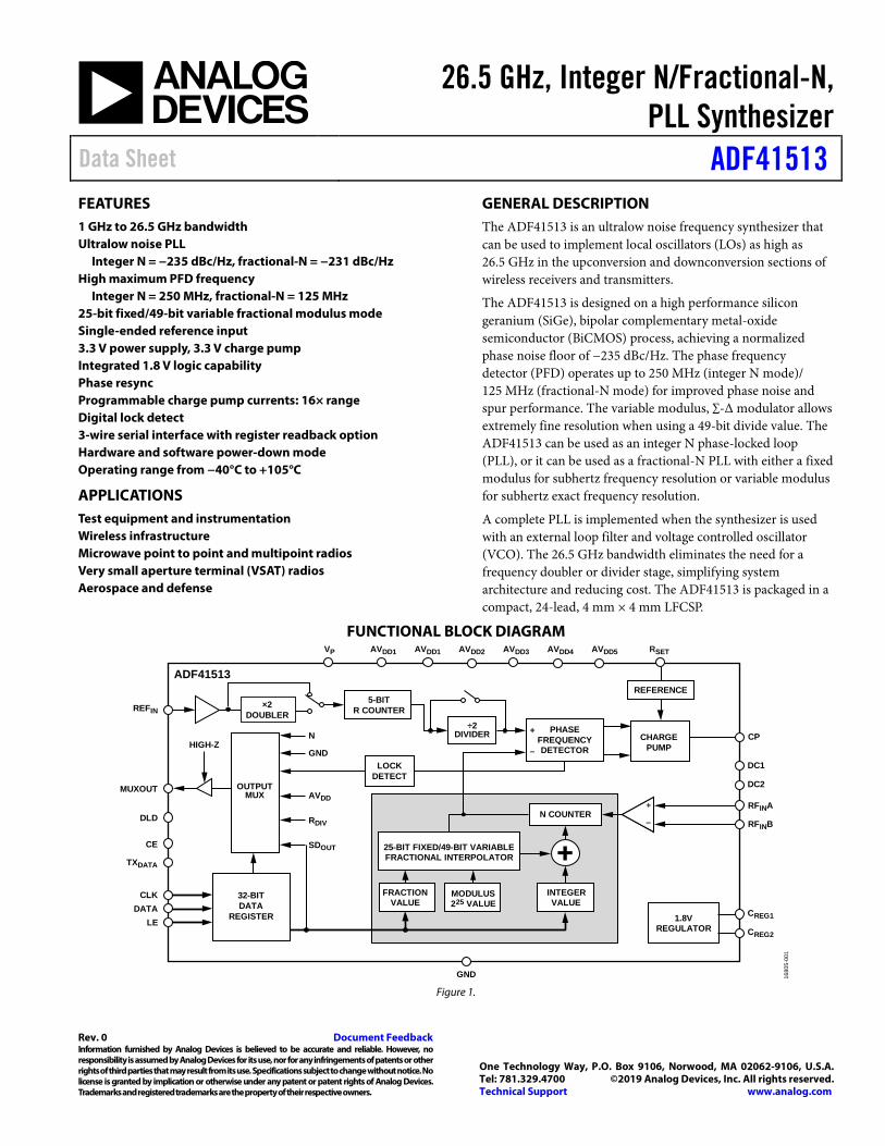
FUNCTIONAL BLOCK DIAGRAM
LOCKDETECT
CP
DATALE
32-BITDATA
REGISTER
CLK
GND
RDIV
AVDD
SDOUT
N
AVDD1 AVDD1 AVDD2 AVDD3 AVDD4 AVDD5
CREG1
GND
CREG2
VP
CE
RFINA
RFINB
OUTPUTMUX
MUXOUT
–
+HIGH-Z
PHASEFREQUENCYDETECTOR
ADF41513
25-BIT FIXED/49-BIT VARIABLEFRACTIONAL INTERPOLATOR
FRACTIONVALUE
INTEGERVALUE
CHARGEPUMP
1.8VREGULATOR
TXDATA
REFERENCE
RSET
REFIN×2
DOUBLER
5-BITR COUNTER
÷2DIVIDER
MODULUS225 VALUE
N COUNTER+
–DLD
DC1
DC216
805-
001
Figure 1.

ADF41513 Data Sheet
Rev. 0 | Page 2 of 30
TABLE OF CONTENTS Features .............................................................................................. 1 Applications ....................................................................................... 1 General Description ......................................................................... 1 Functional Block Diagram .............................................................. 1 Revision History ............................................................................... 2 Specifications ..................................................................................... 3
Timing Characteristics ................................................................ 5 Absolute Maximum Ratings ............................................................ 6
Thermal Resistance ...................................................................... 6 ESD Caution .................................................................................. 6
Pin Configuration and Function Description .............................. 7 Typical Performance Characteristics ............................................. 9 Theory of Operation ...................................................................... 11
Reference Input ........................................................................... 11 RF Input Stage ............................................................................. 11 N Divider and R Counter .......................................................... 11 R Counter .................................................................................... 12 PFD and Charge Pump .............................................................. 12 MUXOUT .................................................................................... 12 Lock Detector .............................................................................. 12 Readback ...................................................................................... 13 Input Shift Registers ................................................................... 13 Program Modes .......................................................................... 13
Register Maps .................................................................................. 14 Register 0 (R0) Map ................................................................... 17 Register 1 (R1) Map ................................................................... 17
Register 2 (R2) Map ................................................................... 18 Register 3 (R3) Map ................................................................... 18 Register 4 (R4) Map ................................................................... 19 Register 5 (R5) Map ................................................................... 19 Register 6 (R6) Map ................................................................... 21 Register 7 (R7) Map ................................................................... 23 Register 8 (R8) Map ................................................................... 24 Register 9 (R9) Map ................................................................... 24 Register 10 (R10) Map ............................................................... 25 Register 11 (R11) Map ............................................................... 25 Register 12 (R12) Map ............................................................... 26 Register 13 (R13) Map ............................................................... 27
Applications information .............................................................. 28 Initialization Sequence .............................................................. 28 RF Synthesizer: A Worked Example of 25-Bit Fixed Modulus Mode ............................................................................................ 28 RF Synthesizer: A Worked Example of Variable Modulus Mode ............................................................................................ 28 Modulus ....................................................................................... 28 Reference Doubler and Reference Divider ............................. 28 Spur Mechanisms ....................................................................... 29 Phase Resync ............................................................................... 29
Outline Dimensions ....................................................................... 30 Ordering Guide .......................................................................... 30
REVISION HISTORY 1/2019—Revision 0: Initial Version
Data Sheet ADF41513
Rev. 0 | Page 3 of 30
SPECIFICATIONS AVDDx = AVDD1 = AVDD2 = AVDD3 = AVDD4 = AVDD5 = VP = 3.3 V ± 5%, GND = 0 V, RSET = 1.8 kΩ, dBm referred to 50 Ω, TA = TMIN (−40°C) to TMAX (+105°C), unless otherwise noted.
Table 1. Parameter Min Typ Max Unit Test Conditions/Comments RADIO FREQUENCY (RF)
CHARACTERISTICS
8/9 Prescaler
RF Input Frequency (fRFIN) Range 1 26.5 GHz Recommended input power of −5 dBm to +5 dBm, operation at this frequency range is limited to 70°C to TMIN
1 24 GHz Operation at this frequency range is TMAX to TMIN RF Input Sensitivity −11 dBm Refer to Figure 10 and Figure 11 for more
information
4/5 Prescaler
fRFIN Range 1 16 GHz For lower frequencies, ensure slew rate > 320 V/µs
RF Input Sensitivity Range −7 +5 dBm Measured single-ended to RFINA via a 1 pF series capacitor, 1 pF capacitor to GND on RFINB
INPUT REFERENCE FREQUENCY (REFIN) CHARACTERISTICS
REFIN Input
Frequency 10 800 MHz
Voltage Range 0 1.8 V
Sensitivity Range −10 8 dBm Biased at 1 V (ac coupling ensures 1 V bias), use square wave at low power and/or frequency to ensure slew rate is > 320 V/µs; for best inband phase noise performance, ensure slew rate > 500 V/µs
Capacitance 10 pF
Current ±150 µA
Doubler Input Frequency 225 MHz Maximum reference frequency when the doubler is enabled
MAXIMUM PFD FREQUENCY
Integer N Mode 250 MHz Fractional-N Mode 125 MHz
N DIVIDER RANGE 16-Bit N Divider Range
Integer N Mode 20 511 4/5 prescaler 64 1023 8/9 prescaler
Fractional-N Mode 23 511 4/5 prescaler 75 1023 8/9 prescaler
CHARGE PUMP (CP) CP Current (ICP) Sink and Source Programmable
High Value 7.2 mA With RSET = 1.8 kΩ
Low Value 0.45 mA
Absolute Accuracy 5 % With RSET = 1.8 kΩ
RSET Range 1.8 2.7 10 kΩ 5% accuracy ICP Three-State Leakage 2 nA VCP = 0.9 V, TA = 25°C
Sink and Source Current Matching 5 % 0.7 V ≤ CP voltage (VCP) ≤ VP − 0.7 V ICP vs. VCP 5 % 0.7 V ≤ VCP ≤ VP − 0.7 V
ICP vs. Temperature 5 % VCP = VP/2

ADF41513 Data Sheet
Rev. 0 | Page 4 of 30
Parameter Min Typ Max Unit Test Conditions/Comments LOGIC INPUTS
Input Voltage High (VIH) 1.4 V The serial port interface (SPI) block can accept
both 1.8 V or 3.3 V logic inputs
Low (VIL) 0.6 V Input Current (IINH, IINL) ±1 µA Input Capacitance (CIN) 10 pF
LOGIC OUTPUTS Output Voltage
High (VOH) 1.4 V MUXOUT voltage = 1.8 V, DLD voltage = 1.8 V 2.6 V MUXOUT voltage = 3.3 V, DLD voltage = 3.3 V
Low (VOL) 0.4 V Output High Current, Output Low
Current (IOH, IOL) 500 µA
POWER SUPPLIES AVDD1, AVDD2, AVDD3, AVDD4, AVDD5, VP 3.135 3.3 3.465 V IDD1
1 2 3.2 mA Current drawn by AVDD1 IDD2
1 63.5 88 mA Current drawn by AVDD2 IDD3
1 2.1 3.6 mA Current drawn by AVDD3 IDD4
1 1.45 2 mA Current drawn by AVDD4 IDD5
1 20 25 mA Current drawn by AVDD5 IP 6 7 mA Current drawn by VP ITOTAL 95.1 128.8 mA Total current drawn by AVDDx and VP
Power-Down Mode 100 µA TA = 25°C, CE is low, total of all rails NOISE CHARACTERISTICS
Normalized Phase Noise Floor (PNSYNTH) In Integer N Mode2 −235 dBc/Hz PLL loop bandwidth (BW) = 1 MHz (Integer N
mode) In Fractional-N Mode3 −231 dBc/Hz PLL loop BW = 1 MHz (fractional-N mode)
Normalized 1∕f Noise (PN1_f)3 −128 dBc/Hz 10 kHz offset, normalized to 1 GHz SPURIOUS SIGNALS
Reference Spurious −90 dBc At reference = 100 MHz, PLL loop BW = 40 kHz PFD Spurious −87 dBc At PFD = 50 MHz, PLL loop BW = 40 kHz
In-Band Integer Boundary Spurious
−45 dBc 10 kHz offset, PLL loop BW = 250 kHz
1 TA = 25°C, AVDDx = 3.3 V (where x = 1, 2, 3, or 4), prescaler (P) = 8/9, fRFIN = 26.5 GHz, REFIN = 124 MHz, PFD frequency input (fPFD) = 124 MHz. 2 The synthesizer phase noise floor is estimated by measuring the inband phase noise at the output of the VCO and subtracting 20 log N (where N is the N divider value)
and 10 log fPFD. PNSYNTH is the total phase noise measured at the VCO output (PNTOT) − 10 log fPFD − 20 log N. 3 The PLL phase noise is composed of 1/f (flicker) noise plus the normalized PLL noise floor. The formula for calculating the 1/f noise contribution at an RF frequency, fRF,
and at a frequency offset, f, is given by phase noise (PN) = P1_f + 10 log(10 kHz/f) + 20 log(fRF/1 GHz). Both the normalized phase noise floor and flicker noise are modeled in the ADIsimPLL.
Data Sheet ADF41513
Rev. 0 | Page 5 of 30
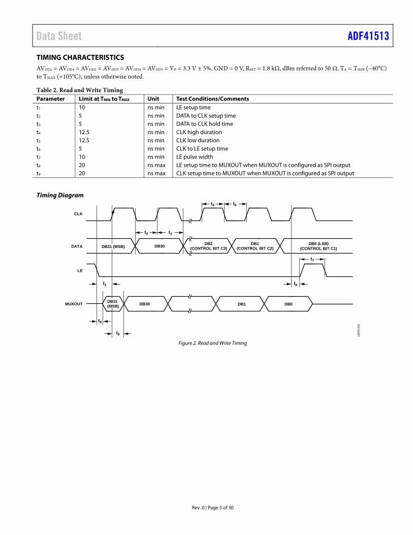
TIMING CHARACTERISTICS AVDDx = AVDD1 = AVDD2 = AVDD3 = AVDD4 = AVDD5 = VP = 3.3 V ± 5%, GND = 0 V, RSET = 1.8 kΩ, dBm referred to 50 Ω, TA = TMIN (−40°C) to TMAX (+105°C), unless otherwise noted.
Table 2. Read and Write Timing Parameter Limit at TMIN to TMAX Unit Test Conditions/Comments t1 10 ns min LE setup time t2 5 ns min DATA to CLK setup time t3 5 ns min DATA to CLK hold time t4 12.5 ns min CLK high duration t5 12.5 ns min CLK low duration t6 5 ns min CLK to LE setup time t7 10 ns min LE pulse width t8 20 ns max LE setup time to MUXOUT when MUXOUT is configured as SPI output t9 20 ns max CLK setup time to MUXOUT when MUXOUT is configured as SPI output
Timing Diagram
CLK
DATA
LE
DB30 DB1(CONTROL BIT C2)
DB2(CONTROL BIT C3)
DB0 (LSB)(CONTROL BIT C1)
t1
t2 t3
t4 t5
t7
t6
DB31 (MSB)
DB0DB1
t8
t9
DB31(MSB) DB30MUXOUT
1680
5-00
2
Figure 2. Read and Write Timing
ADF41513 Data Sheet
Rev. 0 | Page 6 of 30
ABSOLUTE MAXIMUM RATINGS TA = 25°C, unless otherwise noted.
Table 3. Parameter Rating AVDDx to GND1 −0.3 V to +3.6 V VP to GND −0.3 V to +3.6 V VP to AVDDx −0.3 V to +0.3 V Digital Input/Output Voltage to GND −0.3 V to AVDDx + 0.3 V Analog Input/Output Voltage to GND −0.3 V to VP + 0.3 V RFINA, RFINB to GND −0.3 V to +3.6 V RFINA to RFINB1 ±1.4 V REFIN to GND −0.3 V to +2.1 V Operating Temperature Range
Industrial −40°C to +105°C Storage Temperature Range −65°C to +125°C Maximum Junction Temperature
Operational 125°C Reflow Soldering
Peak Temperature 260°C Time at Peak Temperature 40 sec
Electrostatic Discharge (ESD) Charged Device Model 1250 V Human Body Model 1500 V
Transistor Count CMOS 215,726 Bipolar 1625
1 Approximately 13 dBm into a 50 Ω input.
Stresses at or above those listed under Absolute Maximum Ratings may cause permanent damage to the product. This is a stress rating only; functional operation of the product at these or any other conditions above those indicated in the operational section of this specification is not implied. Operation beyond the maximum operating conditions for extended periods may affect product reliability.
This device is a high performance RF IC with an electrostatic discharge (ESD) rating of <2 kV, and the device is ESD sensitive. Take proper precautions for handling and assembly.
THERMAL RESISTANCE Thermal performance is directly linked to printed circuit board (PCB) design and operating environment. Careful attention to PCB thermal design is required.
θJA is the natural convection junction to ambient thermal resistance measured in a one cubic foot sealed enclosure. θJC is the junction to case thermal resistance.
Table 4. Thermal Resistance Package Type θJA θJC Unit CP-24-81 48 38 °C/W 1 The thermal resistance values are defined per the JESD51 standard.
ESD CAUTION

Data Sheet ADF41513
Rev. 0 | Page 7 of 30
PIN CONFIGURATION AND FUNCTION DESCRIPTION
21
3456
181716151413AVDD2
RFINARFINBAVDD1
AVDD1
GND
CECLKDATALEMUXOUTCREG1
8 9 10 117A
V DD
4A
V DD
5R
EFIN
DLD
12TX
DA
TA
AV D
D3
20 1921D
C1
CR
EG2
DC
222
V P
23R
SET
24C
P
ADF41513TOP VIEW
(Not to Scale)
1680
5-00
3NOTES1. EXPOSED PAD. THE EXPOSED PAD MUST
BE CONNECTED TO GND. Figure 3. Pin Configuration
Table 5. Pin Function Descriptions Pin No. Mnemonic Description 1 GND Ground Pin. 2, 3 AVDD1 PFD and Up and Down Digital Driver Power Supply. Pin 2 and Pin 3 can be tied together. With Pin 2 and Pin 3 tied
together, place three parallel capacitors as close as possible to the AVDD1 pins: 10 µF, 100 nF, and 100 pF. 4 RFINB Complementary Input to the RF Prescaler. In single-ended mode, decouple this pin to the ground plane with a
small bypass capacitor, typically 100 pF. 5 RFINA Input to the RF Prescaler. AC-couple this signal to the external VCO. 6 AVDD2 RF Buffer and Prescaler Power Supply. Place three parallel capacitors as close as possible to the AVDD2 pin: 10 µF,
100 nF, and 100 pF. 7 AVDD3 N Divider Power Supply. Place three parallel capacitors as close as possible to the AVDD3 pin: 10 µF, 100 nF, and
100 pF. 8 AVDD4 R Divider and Lock Detector Power Supply. Place three parallel capacitors as close as possible to the AVDD4 pin:
10 µF, 1 µF, and 100 nF. Pin 8 powers the internal low dropout (LDO) regulator for the reference divider. 9 AVDD5 Σ-Δ Modulator and SPI Power Supply. Place three parallel capacitors as close as possible to the AVDD5 pin: 10 µF,
1 µF, and 100 nF. This pin powers the internal LDO regulator for the Σ-Δ modulator. 10 REFIN Reference Input. The reference can accept either a single-ended CMOS (dc-coupled) or single-ended sine wave
(ac-coupled). The single-ended input has a nominal threshold of 1 V and a dc equivalent input resistance of 20 kΩ. 11 DLD Digital Lock Detect Pin. A logic high on this pin indicates PLL lock. 12 TXDATA Transmit Data Pin. Pin 12 is not used. Connect Pin 12 to GND. 13 CE Chip Enable. A logic low on this pin powers down the device and puts the charge pump output into three-state
mode. Registers do not hold their values when CE is low. This pin only supports 3.3 V logic inputs. 14 CLK Serial Clock Input. CLK clocks in the serial data to the registers. The data is latched into the 32-bit shift register on
the CLK rising edge. This input is a high impedance CMOS input. 15 DATA Serial Data Input. The serial data is loaded most significant bit (MSB) first with the two least significant bits (LSBs) as
the control bits. This input is a high impedance CMOS input. 16 LE Load Enable, CMOS Input. When LE goes high, the data stored in the shift registers is loaded into one of the four
latches. Select the latch using the control bits. 17 MUXOUT Multiplexer Output. This multiplexer output allows the lock detect, the scaled RF, the scaled reference frequency,
logic high, logic low, or register readback data to be accessed externally. 18 CREG1 Internal 1.8 V Regulator Output Pin. Place three parallel capacitors as close to the CREG1 pin as possible: 4.7 µF,
100 nF, and 1 nF. 19 CREG2 Internal 1.8 V Regulator Output Pin. Place three parallel capacitors as close to the CREG2 pin as possible: 4.7 µF,
100 nF, and 1 nF. 20 DC1 DC Bias Pin 1. Place a 1 µF capacitor in parallel with a 1 nF capacitor to ground, as close as possible to the DC1 pin. 21 DC2 DC Bias Pin 2. Place a 1 µF capacitor in parallel with a 1 nF capacitor to ground, as close as possible to the DC2 pin. 22 VP Charge Pump Power Supply. 23 RSET Maximum Charge Pump Current Setting Resistor. Connecting a resistor between the RSET pin and GND sets the
maximum charge pump output current. The nominal voltage potential at the RSET pin is 0.66 V. The relationship between ICP and RSET is ICP_MAX = 12.96/RSET. For example, with RSET = 2.7 kΩ, ICP MAX = 4.8 mA. The relationship between bleed current (IBLEED) and RSET is IBLEED_MIN = 0.0103/RSET. For example, with RSET = 2.7 kΩ, IBLEED_MIN = 3.81 µA.
ADF41513 Data Sheet
Rev. 0 | Page 8 of 30
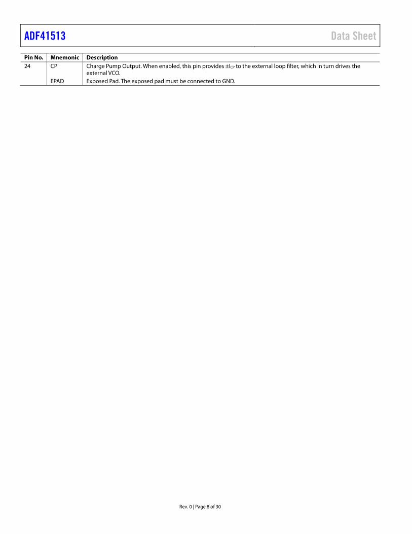
Pin No. Mnemonic Description 24 CP Charge Pump Output. When enabled, this pin provides ±ICP to the external loop filter, which in turn drives the
external VCO. EPAD Exposed Pad. The exposed pad must be connected to GND.
Data Sheet ADF41513
Rev. 0 | Page 9 of 30
TYPICAL PERFORMANCE CHARACTERISTICS
–180
–160
–140
–120
–100
–80
–60
100 1k 10k 100k 1M 10M 100M
PHA
SEN
OIS
E(d
Bc /
Hz)
OFFSET FREQUENCY (Hz) 1680
5-00
4
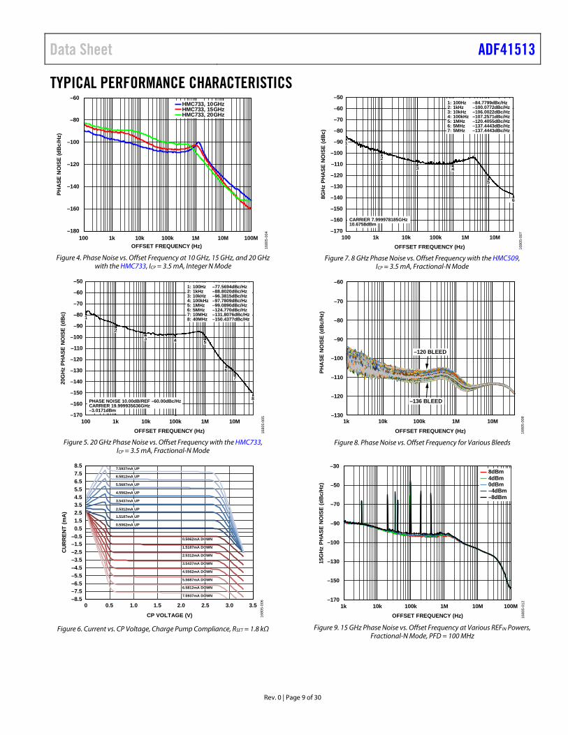
HMC733, 10GHzHMC733, 15GHzHMC733, 20GHz
Figure 4. Phase Noise vs. Offset Frequency at 10 GHz, 15 GHz, and 20 GHz
with the HMC733, ICP = 3.5 mA, Integer N Mode
–50
–60
–70
–80
–90
–100
–110
20G
Hz
PHA
SE N
OIS
E (d
Bc)
–120
–130
–140
–150
–160
–170100 1k 10k 100k
OFFSET FREQUENCY (Hz)1M 10M
2
1
3 4 5
67
8
1: 100Hz –77.5694dBc/Hz2: 1kHz –88.8020dBc/Hz3: 10kHz –96.3815dBc/Hz4: 100kHz –97.7809dBc/Hz5: 1MHz –99.0890dBc/Hz6: 5MHz –124.770dBc/Hz7: 10MHz –131.8076dBc/Hz8: 40MHz –150.4377dBc/Hz
PHASE NOISE 10.00dB/REF –60.00dBc/HzCARRIER 19.999935636GHz–3.0171dBm
1680
5-00
5
Figure 5. 20 GHz Phase Noise vs. Offset Frequency with the HMC733,
ICP = 3.5 mA, Fractional-N Mode
–8.5–7.5–6.5–5.5–4.5–3.5–2.5–1.5–0.50.51.52.53.54.55.56.57.58.5
0 0.5 1.0 1.5 2.0 2.5 3.0 3.5
CP VOLTAGE (V)
CU
RR
ENT
(mA
)
1680
5-00
6
0.5062mA DOWN
1.5187mA DOWN
2.5312mA DOWN
3.5437mA DOWN
4.5562mA DOWN
5.5687mA DOWN
6.5812mA DOWN
7.5937mA DOWN
0.5062mA UP
1.5187mA UP
2.5312mA UP
3.5437mA UP
4.5562mA UP
5.5687mA UP
6.5812mA UP
7.5937mA UP
Figure 6. Current vs. CP Voltage, Charge Pump Compliance, RSET = 1.8 kΩ
–50
–60
–70
–80
–90
–100
–110
8GH
z PH
ASE
NO
ISE
(dB
c)
–120
–130
–140
–150
–160
–170100 1k 10k 100k
OFFSET FREQUENCY (Hz)1M 10M
2
1
3 4
5
6
1: 100Hz –84.7799dBc/Hz2: 1kHz –100.0772dBc/Hz3: 10kHz –106.0022dBc/Hz4: 100kHz –107.2571dBc/Hz5: 1MHz –120.4055dBc/Hz6: 5MHz –137.4443dBc/Hz7: 5MHz –137.4443dBc/Hz
CARRIER 7.999978185GHz10.6758dBm
1680
5-00
7
Figure 7. 8 GHz Phase Noise vs. Offset Frequency with the HMC509,
ICP = 3.5 mA, Fractional-N Mode
–130
–120
–110
–100
–90
–80
–70
–60
1k 10k 100k 1M 10M
PHA
SEN
OIS
E(d
Bc/
Hz)
OFFSET FREQUENCY (Hz)
–120 BLEED
–136 BLEED
1680
5-00
8
Figure 8. Phase Noise vs. Offset Frequency for Various Bleeds
–170
–150
–130
–100
–90
–70
–50
–30
1k 10k 100k 1M 10M 100M
15G
Hz
PHA
SE N
OIS
E (d
Bc/
Hz)
OFFSET FREQUENCY (Hz)
0dBm4dBm8dBm
–4dBm–8dBm
1680
5-01
2
Figure 9. 15 GHz Phase Noise vs. Offset Frequency at Various REFIN Powers,
Fractional-N Mode, PFD = 100 MHz
ADF41513 Data Sheet
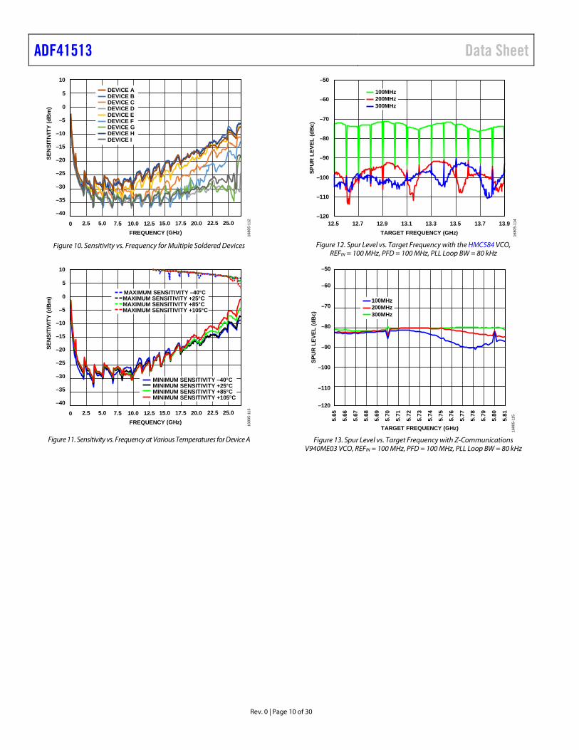
Rev. 0 | Page 10 of 30
–40
–35
–30
–25
–20
–15
–10
–5
0
5
10
0 2.5 5.0 7.5 10.0 12.5 15.0 17.5 20.0 22.5 25.0
SEN
SITI
VITY
(dB
m)
FREQUENCY (GHz)
DEVICE BDEVICE CDEVICE DDEVICE EDEVICE FDEVICE GDEVICE HDEVICE I
DEVICE A
1680
5-11
2
Figure 10. Sensitivity vs. Frequency for Multiple Soldered Devices
–40
–35
–30
–25
–20
–15
–10
–5
0
5
10
0 2.5 5.0 7.5 10.0 12.5 15.0 17.5 20.0 22.5 25.0
SEN
SITI
VITY
(dB
m)
FREQUENCY (GHz)
MINIMUM SENSITIVITY –40°CMINIMUM SENSITIVITY +25°CMINIMUM SENSITIVITY +85°CMINIMUM SENSITIVITY +105°C
MAXIMUM SENSITIVITY –40°CMAXIMUM SENSITIVITY +25°CMAXIMUM SENSITIVITY +85°CMAXIMUM SENSITIVITY +105°C
1680
5-11
3
Figure 11. Sensitivity vs. Frequency at Various Temperatures for Device A
–120
–110
–100
–90
–80
–70
–60
–50
12.5 12.7 12.9 13.1 13.3 13.5 13.7 13.9
SPU
R L
EVEL
(dB
c)
TARGET FREQUENCY (GHz)
100MHz200MHz300MHz
1680
5-11
4
Figure 12. Spur Level vs. Target Frequency with the HMC584 VCO,
REFIN = 100 MHz, PFD = 100 MHz, PLL Loop BW = 80 kHz
–120
–110
–100
–90
–80
–70
–60
–50
5.65
5.66
5.67
5.68
5.69
5.70
5.71
5.72
5.73
5.74
5.75
5.76
5.77
5.78
5.79
5.80
5.81
SPU
R L
EVEL
(dB
c)
TARGET FREQUENCY (GHz)
300MHz200MHz100MHz
1680
5-11
5
Figure 13. Spur Level vs. Target Frequency with Z-Communications
V940ME03 VCO, REFIN = 100 MHz, PFD = 100 MHz, PLL Loop BW = 80 kHz
Data Sheet ADF41513
Rev. 0 | Page 11 of 30
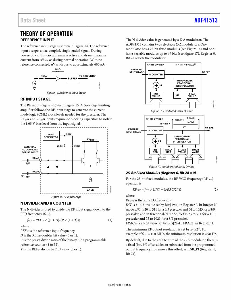
THEORY OF OPERATION REFERENCE INPUT The reference input stage is shown in Figure 14. The reference input accepts an ac-coupled, single-ended signal. During power-down, this circuit remains active and draws the same current from AVDD4 as during normal operation. With no reference connected, AVDD4 drops to approximately 600 μA.
BUFFERTO R COUNTERREFIN
20kΩ
1680
5-01
4
Figure 14. Reference Input Stage
RF INPUT STAGE The RF input stage is shown in Figure 15. A two-stage limiting amplifier follows the RF input stage to generate the current mode logic (CML) clock levels needed for the prescaler. The RFINA and RFINB inputs require dc blocking capacitors to isolate the 1.65 V bias level from the input signal.
BIASGENERATOR
1.65V
AGND
AVDD2
768Ω 768Ω
RFINA
RFINB
1pF
1pF
EXTERNALAC COUPLINGFOR SE INPUT
1680
5-01
5
Figure 15. RF Input Stage
N DIVIDER AND R COUNTER The N divider is used to divide the RF input signal down to the PFD frequency (fPFD).
fPFD = REFIN × ((1 + D)/(R × (1 + T))) (1)
where: REFIN is the reference input frequency. D is the REFIN doubler bit value (0 or 1). R is the preset divide ratio of the binary 5-bit programmable reference counter (1 to 32). T is the REFIN divide by 2 bit value (0 or 1).
The N divider value is generated by a Σ-Δ modulator. The ADF41513 contains two selectable Σ-Δ modulators. One modulator has a 25-bit fixed modulus (see Figure 16) and one has a variable modulus up to 49 bits (see Figure 17). Register 0, Bit 28 selects the modulator.
THIRD-ORDERFRACTIONAL
INTERPOLATOR
FRACVALUE225INT
VALUE
RF INT DIVIDER N = INT + FRAC/225
FROM RFINPUT STAGE TO PFD
N COUNTER
1680
5-01
6
Figure 16. Fixed Modulus N Divider
THIRD-ORDERFRACTIONAL
INTERPOLATOR
MOD2VALUE
INTREG
FRAC2VALUE
FRAC1REG
RF INT DIVIDER
FROM RFINPUT STAGE
TO PFDN COUNTER
N = INT +
FRAC1 +FRAC2
MOD2
2
1680
5-01
7
Figure 17. Variable Modulus N Divider
25-Bit Fixed Modulus (Register 0, Bit 28 = 0)
For the 25-bit fixed modulus, the RF VCO frequency (RFOUT) equation is
RFOUT = fPFD × (INT + (FRAC/225)) (2)
where: RFOUT is the RF VCO frequency. INT is a 16-bit value set by Bits[19:4] in Register 0. In Integer N mode, INT is 20 to 511 for a 4/5 prescaler and 64 to 1023 for a 8/9 prescaler, and in fractional-N mode, INT is 23 to 511 for a 4/5 prescaler and 75 to 1023 for a 8/9 prescaler. FRAC is a 25-bit value set by Bits[28:4], FRAC1, in Register 1.
The minimum RF output resolution is set by fPFD/225. For example, if fPFD = 100 MHz, the minimum resolution is 2.98 Hz.
By default, due to the architecture of the Σ-Δ modulator, there is a fixed (fPFD/226) offset added or subtracted from the programmed output frequency. To remove this offset, set LSB_PI (Register 5, Bit 24).
ADF41513 Data Sheet
Rev. 0 | Page 12 of 30
Variable Modulus (R0, DB28 = 1)
For the variable modulus, the RF VCO frequency (RFOUT) equation is
RFOUT = fPFD × (INT + (FRAC1 + (FRAC2/MOD2))/225) (3)
where: RFOUT is the output frequency of external VCO. INT is a 16-bit value set by Bits[19:4] in Register 0. In Integer N mode, INT is 20 to 511 for a 4/5 prescaler and 64 to 1023 for a 8/9 prescaler, and in fractional-N mode, INT is 23 to 511 for a 4/5 prescaler and 75 to 1023 for a 8/9 prescaler. FRAC1 is a 25-bit value set by Bits[28:4] in Register 1. FRAC2 is a 24-bit value set by Bits[27:4] in Register 3. MOD2 is a 24-bit value set by Bits[27:4] in Register 4.
The minimum RF output resolution is set by fPFD/249. Therefore, for fPFD = 100 MHz, the minimum resolution is 0.1776 µHz. To achieve this resolution, MOD2 must be set to its maximum of (224 − 1), which is 16,777,215.
Integer N Mode
When FRAC1 and FRAC2 are both equal to 0, the ADF41513 can operate in purely integer N mode, which improves the phase noise performance of the PLL and sets the frequency resolution to fPFD. This feature is not automatic and must be manually set for Integer N channels. Bleed must also be disabled when using the ADF41513 in Integer N operation. See the Register 12 (R12) Map section for more information on programming the ADF41513 for Integer N operation.
R COUNTER The 5-bit R counter allows REFIN to be divided down to produce the reference clock to the PFD. Division ratios from 1 to 32 are allowed.
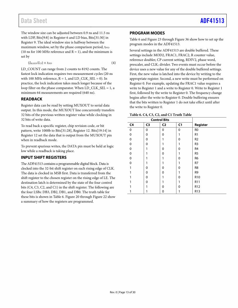
PFD AND CHARGE PUMP The PFD takes inputs from the R counter and N counter and produces an output proportional to the phase and frequency difference between these inputs. Figure 18 shows a PFD simplified schematic. The PFD includes a fixed delay element that sets the width of the antibacklash pulse, which is typically 1 ns. This pulse ensures that there is no dead zone in the PFD transfer function and produces a consistent reference spur level.
U3
CLR2Q2D2
U2
DOWN
UPHIGH
HIGH
CP
–IN
+IN
CHARGEPUMP
DELAY
CLR1
Q1D1
U1
1680
5-01
8
Figure 18. PFD Simplified Schematic
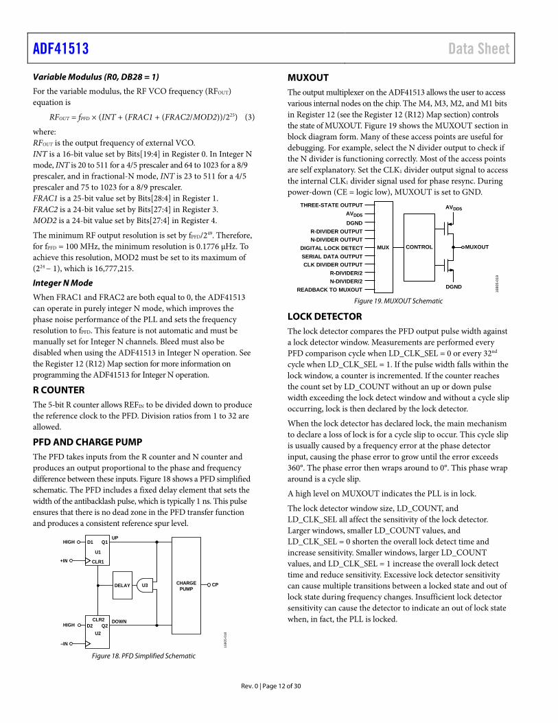
MUXOUT The output multiplexer on the ADF41513 allows the user to access various internal nodes on the chip. The M4, M3, M2, and M1 bits in Register 12 (see the Register 12 (R12) Map section) controls the state of MUXOUT. Figure 19 shows the MUXOUT section in block diagram form. Many of these access points are useful for debugging. For example, select the N divider output to check if the N divider is functioning correctly. Most of the access points are self explanatory. Set the CLK1 divider output signal to access the internal CLK1 divider signal used for phase resync. During power-down (CE = logic low), MUXOUT is set to GND.
THREE-STATE OUTPUT
DGNDR-DIVIDER OUTPUTN-DIVIDER OUTPUT
DIGITAL LOCK DETECTSERIAL DATA OUTPUTCLK DIVIDER OUTPUT
R-DIVIDER/2
MUX CONTROL MUXOUT
AVDD5
DGNDN-DIVIDER/2
READBACK TO MUXOUT
AVDD5
1680
5-01
9
Figure 19. MUXOUT Schematic
LOCK DETECTOR The lock detector compares the PFD output pulse width against a lock detector window. Measurements are performed every PFD comparison cycle when LD_CLK_SEL = 0 or every 32nd cycle when LD_CLK_SEL = 1. If the pulse width falls within the lock window, a counter is incremented. If the counter reaches the count set by LD_COUNT without an up or down pulse width exceeding the lock detect window and without a cycle slip occurring, lock is then declared by the lock detector.
When the lock detector has declared lock, the main mechanism to declare a loss of lock is for a cycle slip to occur. This cycle slip is usually caused by a frequency error at the phase detector input, causing the phase error to grow until the error exceeds 360°. The phase error then wraps around to 0°. This phase wrap around is a cycle slip.
A high level on MUXOUT indicates the PLL is in lock.
The lock detector window size, LD_COUNT, and LD_CLK_SEL all affect the sensitivity of the lock detector. Larger windows, smaller LD_COUNT values, and LD_CLK_SEL = 0 shorten the overall lock detect time and increase sensitivity. Smaller windows, larger LD_COUNT values, and LD_CLK_SEL = 1 increase the overall lock detect time and reduce sensitivity. Excessive lock detector sensitivity can cause multiple transitions between a locked state and out of lock state during frequency changes. Insufficient lock detector sensitivity can cause the detector to indicate an out of lock state when, in fact, the PLL is locked.
Data Sheet ADF41513
Rev. 0 | Page 13 of 30
The window size can be adjusted between 0.9 ns and 11.5 ns with LDP, Bits[9:8] in Register 6 and LD bias, Bits[31:30] in Register 9. The ideal window size is halfway between the maximum window, set by the phase comparison period, tPFD (10 ns for 100 MHz reference and R = 1), and the minimum is set by
(IBLEED/ICP) × tPFD (4)
LD_COUNT can range from 2 counts to 8192 counts. The fastest lock indication requires two measurement cycles (20 ns with 100 MHz reference, R = 1, and LD_CLK_SEL = 0). In practice, the lock indication takes much longer because of the loop filter on the phase comparator. When LD_CLK_SEL = 1, a minimum 64 measurements are required (640 ns).
READBACK Register data can be read by setting MUXOUT to serial data output. In this mode, the MUXOUT line concurrently transfers 32 bits of the previous written register value while clocking in 32 bits of write data.
To read back a specific register, chip revision code, or bit pattern, write 1000b to Bits[31:28], Register 12. Bits[19:14] in Register 12 set the data that is output from the MUXOUT pin when in readback mode.
To prevent spurious writes, the DATA pin must be held at logic low while a readback is taking place.
INPUT SHIFT REGISTERS The ADF41513 contains a programmable digital block. Data is clocked into the 32-bit shift register on each rising edge of CLK. The data is clocked in MSB first. Data is transferred from the shift register to the chosen register on the rising edge of LE. The destination latch is determined by the state of the four control bits (C4, C3, C2, and C1) in the shift register. The following are the four LSBs: DB3, DB2, DB1, and DB0. The truth table for these bits is shown in Table 6. Figure 20 through Figure 22 show a summary of how the registers are programmed.
PROGRAM MODES Table 6 and Figure 23 through Figure 36 show how to set up the program modes in the ADF41513.
Several settings in the ADF41513 are double buffered. These settings include MOD2, FRAC1, FRAC2, R counter value, reference doubler, CP current setting, RDIV2, phase word, prescaler, and CLK1 divider. Two events must occur before the device uses a new value for any of the double buffered settings. First, the new value is latched into the device by writing to the appropriate register. Second, a new write must be performed on Register 0. For example, updating the FRAC1 value requires a write to Register 1 and a write to Register 0. Write to Register 1 first, followed by the write to Register 0. The frequency change begins after the write to Register 0. Double buffering ensures that the bits written to Register 1 do not take effect until after the write to Register 0.
Table 6. C4, C3, C2, and C1 Truth Table Control Bits
C4 C3 C2 C1 Register 0 0 0 0 R0 0 0 0 1 R1 0 0 1 0 R2 0 0 1 1 R3 0 1 0 0 R4 0 1 0 1 R5 0 1 1 0 R6 0 1 1 1 R7 1 0 0 0 R8 1 0 0 1 R9 1 0 1 0 R10 1 0 1 1 R11 1 1 0 0 R12 1 1 0 1 R13
ADF41513 Data Sheet
Rev. 0 | Page 14 of 30
REGISTER MAPS
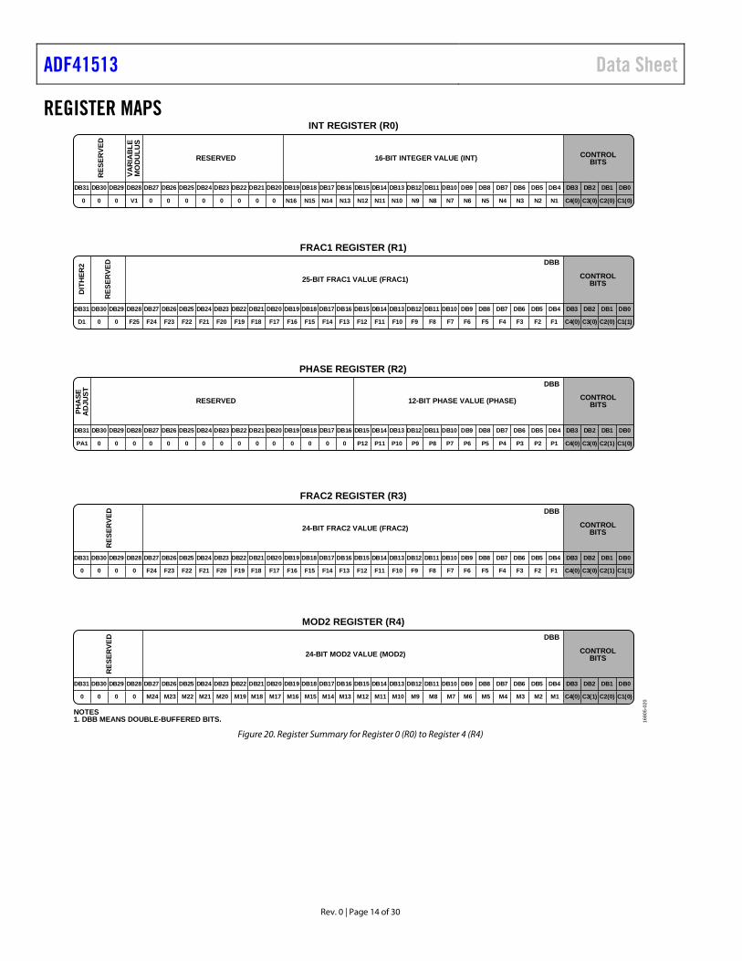
DB31
CONTROLBITS16-BIT INTEGER VALUE (INT)RESERVED
DB30 D DB29 B28 DB27 DB26 DB25 DB24 DB23 DB22 DB21 DB20 DB19 DB18 DB17 DB16 DB15 DB14 DB13 DB12 DB11 DB10 DB9 DB8 DB7 DB6 DB5 DB4 DB3 DB2 DB1 DB0
0 V1 00000 0 0 0 0 0 N1N2N3N4N5N6N7N8N9N10N11N12N13N14N15N16 C3(0)C4(0) C2(0) C1(0)
VAR
IAB
LEM
OD
ULU
SINT REGISTER (R0)
FRAC1 REGISTER (R1)
FRAC2 REGISTER (R3)
PHASE REGISTER (R2)
DBB
DBB
RES
ERVE
D
DB31
CONTROLBITS25-BIT FRAC1 VALUE (FRAC1)
DB30 D DB29 B28 DB27 DB26 DB25 DB24 DB23 DB22 DB21 DB20 DB19 DB18 DB17 DB16 DB15 DB14 DB13 DB12 DB11 DB10 DB9 DB8 DB7 DB6 DB5 DB4 DB3 DB2 DB1 DB0
00D1 F1F2F3F4F5F6F8 F7F9F10F11F12F13F14F15F16F17F18F19F20F21F22F23F24F25 C3(0)C4(0) C2(0) C1(1)
RES
ERVE
D
DIT
HER
2
DB31
CONTROLBITS12-BIT PHASE VALUE (PHASE)RESERVED
DB30 D DB29 B28 DB27 DB26 DB25 DB24 DB23 DB22 DB21 DB20 DB19 DB18 DB17 DB16 DB15 DB14 DB13 DB12 DB11 DB10 DB9 DB8 DB7 DB6 DB5 DB4 DB3 DB2 DB1 DB0
PA1 000000 0 0 0 0 0 0 0 0 0 P1P2P3P4P5P6P7P8P9P10P11P12 C3(0)C4(0) C2(1) C1(0)
PHA
SEA
DJU
ST
DBB
DB31
CONTROLBITS24-BIT FRAC2 VALUE (FRAC2)
DB30 D DB29 B28 DB27 DB26 DB25 DB24 DB23 DB22 DB21 DB20 DB19 DB18 DB17 DB16 DB15 DB14 DB13 DB12 DB11 DB10 DB9 DB8 DB7 DB6 DB5 DB4 DB3 DB2 DB1 DB0
000 F1F2F3F4F5F6F8 F7F9F10F11F12F13F14F15F16F17F18F19F20F21F22F23F240 C3(0)C4(0) C2(1) C1(1)
RES
ERVE
D
MOD2 REGISTER (R4)
NOTES1. DBB MEANS DOUBLE-BUFFERED BITS.
DBB
DB31
CONTROLBITS24-BIT MOD2 VALUE (MOD2)
DB30 D DB29 B28 DB27 DB26 DB25 DB24 DB23 DB22 DB21 DB20 DB19 DB18 DB17 DB16 DB15 DB14 DB13 DB12 DB11 DB10 DB9 DB8 DB7 DB6 DB5 DB4 DB3 DB2 DB1 DB0
000 M1M2M3M4M5M6M8 M7M9M10M11M12M13M14M15M16M17M18M19M20M21M22M23M240 C3(1)C4(0) C2(0) C1(0)
RES
ERVE
D
1680
5-02
0
Figure 20. Register Summary for Register 0 (R0) to Register 4 (R4)
Data Sheet ADF41513
Rev. 0 | Page 15 of 30
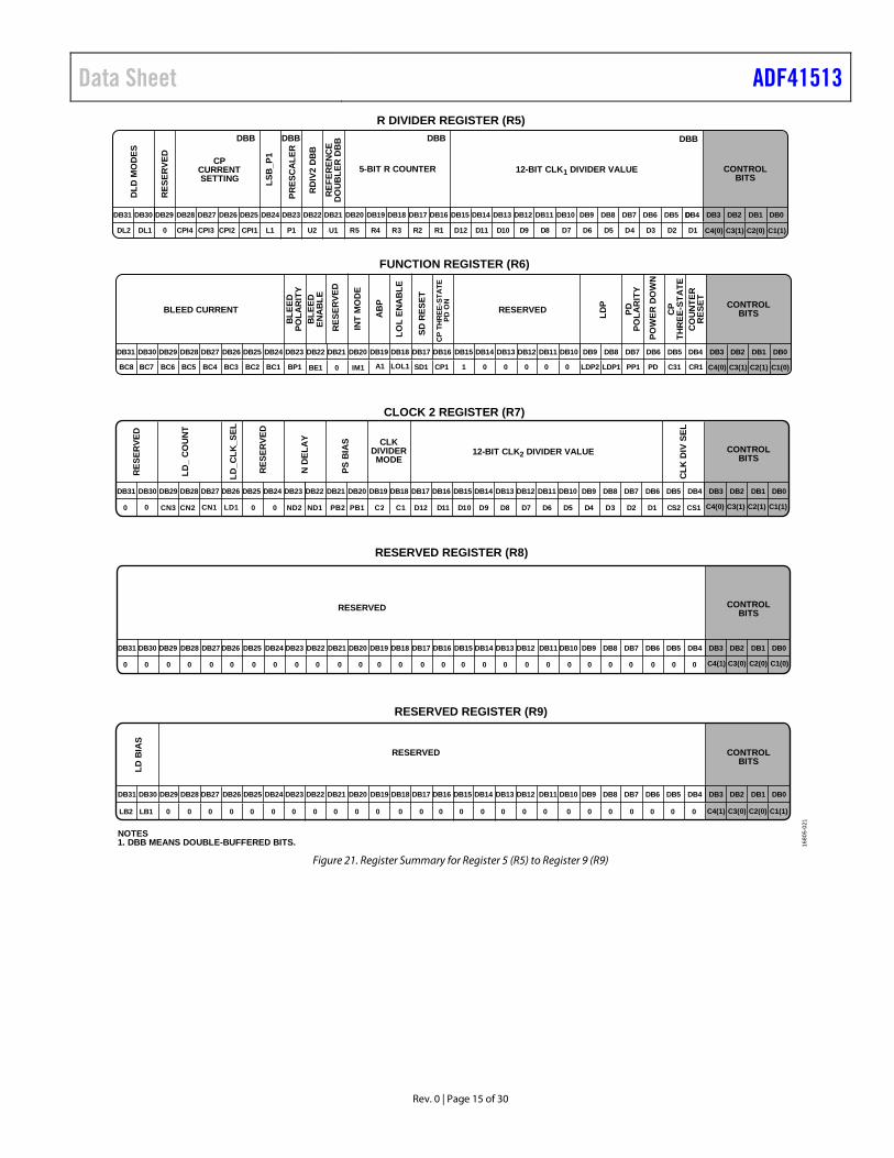
5-BIT R COUNTER
LSB
_P1
PRES
CA
LER
RES
ERVE
D
DLD
MO
DES
RD
IV2
DB
B
D
DL2 DL1 0 CPI4 CPI3 CPI2 CPI1 P1 U2 U1 R5 R4 R3 R2 R1 D12 D11 D10 D9 D8 D7 D6 D5 D4 D3 D2 D1
R DIVIDER REGISTER (R5)DBB DBB DBB DBB
CONTROLBITS
12-BIT CLK1 DIVIDER VALUECP
CURRENTSETTING
REF
EREN
CE
DO
UB
LER
DB
B
L1
BLEED CURRENT
POW
ER D
OW
N
PDPO
LAR
ITY
LDP
CO
UN
TER
RES
ET
CP
THR
EE-S
TATE
BC7BC8 BC6 BC5 BC4 BC3 BC2 BC1 BP1 BE1 0 IM1 A1 LOL1 SD1 CP1 1 0 0 0 LDP1 PP1 PD C31 CR1
FUNCTION REGISTER (R6)
CLOCK 2 REGISTER (R7)
CP
THR
EE-S
TATE
PD O
N
LOL
ENA
BLE
AB
P
INT
MO
DE
RES
ERVE
D
RESERVED
BLE
EDPO
LAR
ITY
BLE
EDEN
AB
LE
SD R
ESET CONTROL
BITS
12-BIT CLK2 DIVIDER VALUE
0 CN3 CN2 CN1 LD1 0 0 ND2 ND1 PB2 PB1 C C1 D12 D11 D10 D9 D8 D7 D6 D5 D4 D3 D2 D1
CLKDIVIDERMODE
CS1CS2
CLK
DIV
SEL
CONTROLBITS
RES
ERVE
D
LD_
CO
UN
T
LD_C
LK_S
EL
RES
ERVE
D
0 0 0
RESERVED REGISTER (R8)
RESERVED CONTROLBITS
RESERVED
LB2 LB1
RESERVED REGISTER (R9)
CONTROLBITS
NOTES1. DBB MEANS DOUBLE-BUFFERED BITS.
0 LDP20
0
0
0 0 0 0 0 0 0 0 0 0 0 0 0 0 0 0 0 0 0 0 0 0 0 0 0 0
00 0 0 0000 0 0 0000 0 0 0000 0000
N D
ELA
Y
PS B
IAS
LD B
IAS
1680
5-02
1
DB31 DB30 DB29 DB28 DB27 DB26 DB25 DB24 DB23 DB22 DB21 DB20 DB19 DB18 DB17 DB16 DB15 DB14 DB13 DB12 DB11 DB10 DB9 DB8 DB7 DB6 DB5 DB4 DB3 DB2 DB1 DB0
C3(1)C4(0) C2(0) C1(1)
DB31 DB30 DB29 DB28 DB27 DB26 DB25 DB24 DB23 DB22 DB21 DB20 DB19 DB18 DB17 DB16 DB15 DB14 DB13 DB12 DB11 DB10 DB9 DB8 DB7 DB6 DB5 DB4 DB3 DB2 DB1 DB0
C3(1)C4(0) C2(1) C1(0)
DB31 DB30 DB29 DB28 DB27 DB26 DB25 DB24 DB23 DB22 DB21 DB20 DB19 DB18 DB17 DB16 DB15 DB14 DB13 DB12 DB11 DB10 DB9 DB8 DB7 DB6 DB5 DB4 DB3 DB2 DB1 DB0
C3(1)C4(0) C2(1) C1(1)
DB31 DB30 DB29 DB28 DB27 DB26 DB25 DB24 DB23 DB22 DB21 DB20 DB19 DB18 DB17 DB16 DB15 DB14 DB13 DB12 DB11 DB10 DB9 DB8 DB7 DB6 DB5 DB4 DB3 DB2 DB1 DB0
C3(0)C4(1) C2(0) C1(0)
DB31 DB30 DB29 DB28 DB27 DB26 DB25 DB24 DB23 DB22 DB21 DB20 DB19 DB18 DB17 DB16 DB15 DB14 DB13 DB12 DB11 DB10 DB9 DB8 DB7 DB6 DB5 DB4 DB3 DB2 DB1 DB0
C3(0)C4(1) C2(0) C1(1)
Figure 21. Register Summary for Register 5 (R5) to Register 9 (R9)
ADF41513 Data Sheet
Rev. 0 | Page 16 of 30
RESERVED
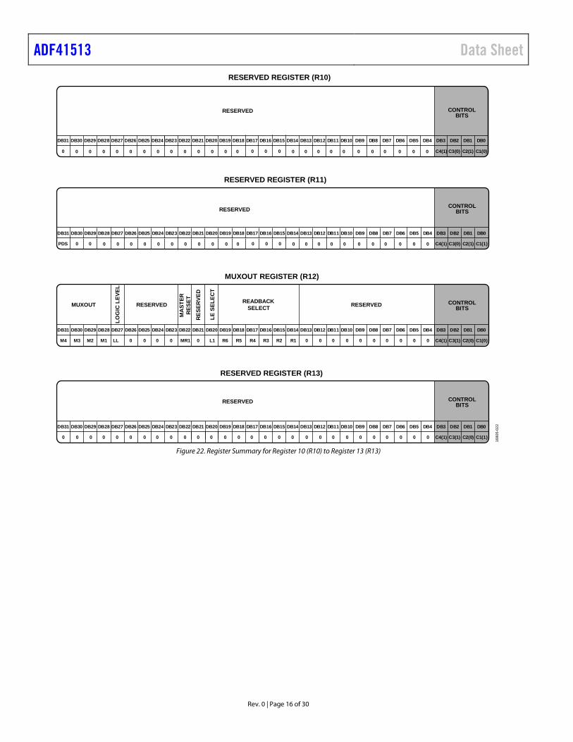
DB31 DB30 DB29 DB28 DB27 DB26 DB25 DB24 DB23 DB22 DB21 DB20 DB19 DB18 DB17 DB16 DB15 DB14 DB13 DB12 DB11 DB10 DB9 DB8 DB7 DB6 DB5 DB4 DB3 DB2 DB1 DB0
0 0 0 0 0 0 0 0 CC4(1) 3(0) C2(1) C1(0)
RESERVED REGISTER (R10)
CONTROLBITS
DB31 DB30 DB29 DB28 DB27 DB26 DB25 DB24 DB23 DB22 DB21 DB20 DB19 DB18 DB17 DB16 DB15 DB14 DB13 DB12 DB11 DB10 DB9 DB8 DB7 DB6 DB5 DB4 DB3 DB2 DB1 DB0
PDS 0 0 CC4(1) 3(0) C2(1) C1(1)
RESERVED REGISTER (R11)
RESERVED CONTROLBITS
DB31
RESERVED
MA
STER
RES
ET
LOG
IC L
EVEL
LE S
ELEC
T
DB30 DB29 DB28 DB27 DB26 DB25 DB24 DB23 DB22 DB21 DB20 DB19 DB18 DB17 DB16 DB15 DB14 DB13 DB12 DB11 DB10 DB9 DB8 DB7 DB6 DB5 DB4 DB3 DB2 DB1 DB0
M4 M3 M2 M1 0 0000LL MR1 L1 R6 R5 R4 R3 R2 R1 0 0 0 0 0 0 0 0 0 0 CC4(1) 3(1) C2(0) C1(0)
MUXOUT REGISTER (R12)
MUXOUT RESERVED
RES
ERVE
D
READBACKSELECT
CONTROLBITS
DB31
RESERVED
DB30 DB29 DB28 DB27 DB26 DB25 DB24 DB23 DB22 DB21 DB20 DB19 DB18 DB17 DB16 DB15 DB14 DB13 DB12 DB11 DB10 DB9 DB8 DB7 DB6 DB5 DB4 DB3 DB2 DB1 DB0
0 0 00000 0 0 000000000 0 0 0 0 0 0 0 0 0 0 CC4(1) 3(1) C2(0) C1(1)
RESERVED REGISTER (R13)
CONTROLBITS
0 0 0 0 0 0 0 00 0 0 0 00 0 0 00 0 0
0 0 0 0 00 0 0 0 0 0 0 00 0 0 0 00 0 0 00 0 0
1680
5-02
2
Figure 22. Register Summary for Register 10 (R10) to Register 13 (R13)
Data Sheet ADF41513
Rev. 0 | Page 17 of 30
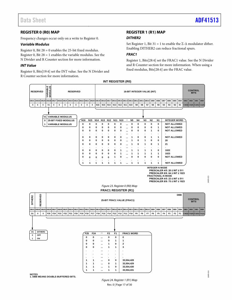
REGISTER 0 (R0) MAP Frequency changes occur only on a write to Register 0.
Variable Modulus
Register 0, Bit 28 = 0 enables the 25-bit fixed modulus. Register 0, Bit 28 = 1 enables the variable modulus. See the N Divider and R Counter section for more information.
INT Value
Register 0, Bits[19:4] set the INT value. See the N Divider and R Counter section for more information.
REGISTER 1 (R1) MAP DITHER2
Set Register 1, Bit 31 = 1 to enable the Σ-Δ modulator dither. Enabling DITHER2 can reduce fractional spurs.
FRAC1
Register 1, Bits[28:4] set the FRAC1 value. See the N Divider and R Counter section for more information. When using a fixed modulus, Bits[28:4] are the FRAC value.
DB31
CONTROLBITS16-BIT INTEGER VALUE (INT)RESERVED
DB30 DB29 DB28 DB27 DB26 DB25 DB24 DB23 DB22 DB21 DB20 DB19 DB18 DB17 DB16 DB15 DB14 DB13 DB12 DB11 DB10 DB9 DB8 DB7 DB6 DB5 DB4 DB3 DB2 DB1 DB0
0 V1 00000 0 0 0 0 0 N1N2N3N4N5N6N7N8N9N10N11N12N13N14N15N16 C3(0)C4(0) C2(0) C1(0)
VAR
IAB
LEM
OD
ULU
S
INT REGISTER (R0)
RESERVED
N16 N15 ... N2 N1 INTEGER WORD
INTEGER N MODE PRESCALER 4/5: 20 ≤ INT ≤ 511 PRESCALER 8/9: 64 ≤ INT ≤ 1023FRACTIONAL-N MODE PRESCALER 4/5: 23 ≤ INT ≤ 511 PRESCALER 8/9: 75 ≤ INT ≤ 1023
0 0 ... 0 0 NOT ALLOWED0 0 ... 0 1 NOT ALLOWED0 0 ... 1 0 NOT ALLOWED
0 0 ... 1 1 NOT ALLOWED. . ... . . .
20
. . ... . . .0 0 ... 0 1 21
0
.0
1.1
.1
.1
.1
.1
.1
.1
.1
.1
.1
.1
.NOT ALLOWED
... 1 0 10220 ... 1 1 1023
...
...
0 0 NOT ALLOWED
V1 VARIABLE MODULUS0 25-BIT FIXED MODULUS
VARIABLE MODULUS1
N4 N30 00 00 0
0 0. .
. .0 1
1 11 10 0
N5000
1.
.1
110
0 0
N14000
0.
.00
N13000
0.
.00
N12000
0.
.00
0
00
0
00
0
00
0
00
N11000
0.
.0
001
0
N10000
0.
.0
110
0 ... 0 00 11
1680
5-02
3
Figure 23. Register 0 (R0) Map
FRAC1 REGISTER (R1)DBB
DB31
CONTROLBITS25-BIT FRAC1 VALUE (FRAC1)
DB30 DB29 DB28 DB27 DB26 DB25 DB24 DB23 DB22 DB21 DB20 DB19 DB18 DB17 DB16 DB15 DB14 DB13 DB12 DB11 DB10 DB9 DB8 DB7 DB6 DB5 DB4 DB3 DB2 DB1 DB0
00D1 F1F2F3F4F5F6F8 F7F9F10F11F12F13F14F15F16F17F18F19F20F21F22F23F24F25 C3(0)C4(0) C2(0) C1(1)
RES
ERVE
D
DIT
HER
2
NOTES1. DBB MEANS DOUBLE-BUFFERED BITS.
F25 F24 ... F2 F1 FRAC1 WORD0 0 ... 0 0 00 0 ... 0 1 10 0 ... 1 0 20 0 ... 1 1 3. . ... . . .. . ... . . .. . ... . . .1 1 ... 0 0 33,554,4281 1 ... 0 1 33,554,4291 1 ... 1 0 33,554,4301 1 ... 1 1 33,554,431
D1 DITHER2
0 OFF
1 ON
1680
5-02
4
Figure 24. Register 1 (R1) Map
ADF41513 Data Sheet
Rev. 0 | Page 18 of 30
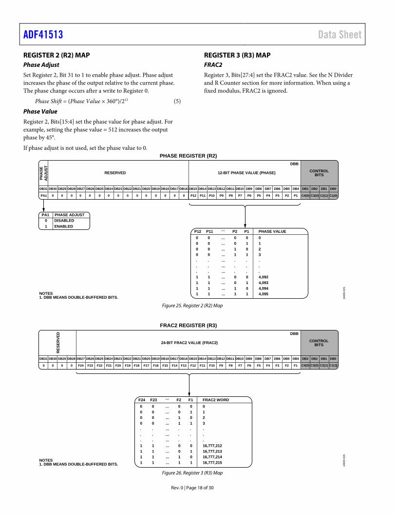
REGISTER 2 (R2) MAP Phase Adjust
Set Register 2, Bit 31 to 1 to enable phase adjust. Phase adjust increases the phase of the output relative to the current phase. The phase change occurs after a write to Register 0.
Phase Shift = (Phase Value × 360°)/212 (5)
Phase Value
Register 2, Bits[15:4] set the phase value for phase adjust. For example, setting the phase value = 512 increases the output phase by 45°.
If phase adjust is not used, set the phase value to 0.
REGISTER 3 (R3) MAP FRAC2
Register 3, Bits[27:4] set the FRAC2 value. See the N Divider and R Counter section for more information. When using a fixed modulus, FRAC2 is ignored.
PHASE REGISTER (R2)DBB
CONTROLBITS12-BIT PHASE VALUE (PHASE)RESERVED
PA1 000000 0 0 0 0 0 0 0 0 0 P1P2P3P4P5P6P7P8P9P10P11P12
PHA
SEA
DJU
ST
NOTES1. DBB MEANS DOUBLE-BUFFERED BITS.
P12 P11 ... P2 P1 PHASE VALUE0 0 ... 0 0 00 0 ... 0 1 10 0 ... 1 0 20 0 ... 1 1 3. . ... . . .. . ... . . .. . ... . . .1 1 ... 0 0 4,0921 1 ... 0 1 4,0931 1 ... 1 0 4,0941 1 ... 1 1 4,095
PHASE ADJUSTPA10 DISABLED1 ENABLED
DB31 DB30 DB29 DB28 DB27 DB26 DB25 DB24 DB23 DB22 DB21 DB20 DB19 DB18 DB17 DB16 DB15 DB14 DB13 DB12 DB11 DB10 DB9 DB8 DB7 DB6 DB5 DB4 DB3 DB2 DB1 DB0
C3(0)C4(0) C2(1) C1(0)
1680
5-02
5
Figure 25. Register 2 (R2) Map
FRAC2 REGISTER (R3)
DBB
CONTROLBITS24-BIT FRAC2 VALUE (FRAC2)
000 F1F2F3F4F5F6F8 F7F9F10F11F12F13F14F15F16F17F18F19F20F21F22F23F240 )
RES
ERVE
D
NOTES1. DBB MEANS DOUBLE-BUFFERED BITS.
F24 F23 ... F2 F1 FRAC2 WORD0 0 ... 0 0 00 0 ... 0 1 10 0 ... 1 0 20 0 ... 1 1 3. . ... . . .. . ... . . .. . ... . . .1 1 ... 0 0 16,777,2121 1 ... 0 1 16,777,2131 1 ... 1 0 16,777,2141 1 ... 1 1 16,777,215
DB31 DB30 DB29 DB28 DB27 DB26 DB25 DB24 DB23 DB22 DB21 DB20 DB19 DB18 DB17 DB16 DB15 DB14 DB13 DB12 DB11 DB10 DB9 DB8 DB7 DB6 DB5 DB4 DB3 DB2 DB1 DB0
C3(0)C4(0) C2(1) C1(1)
1680
5-02
6
Figure 26. Register 3 (R3) Map
Data Sheet ADF41513
Rev. 0 | Page 19 of 30
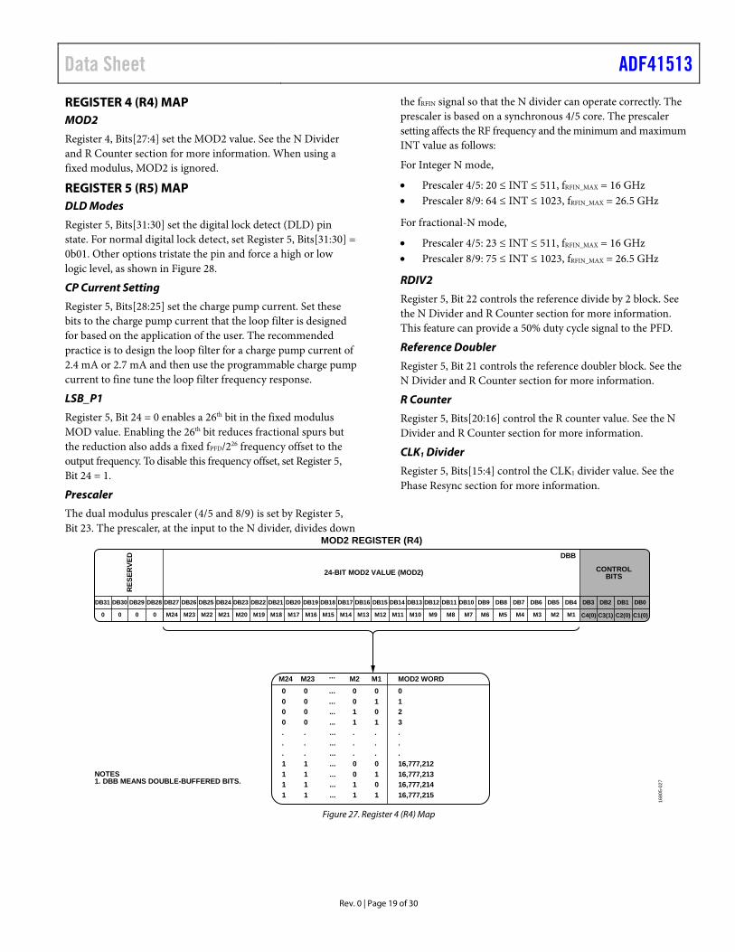
REGISTER 4 (R4) MAP MOD2
Register 4, Bits[27:4] set the MOD2 value. See the N Divider and R Counter section for more information. When using a fixed modulus, MOD2 is ignored.
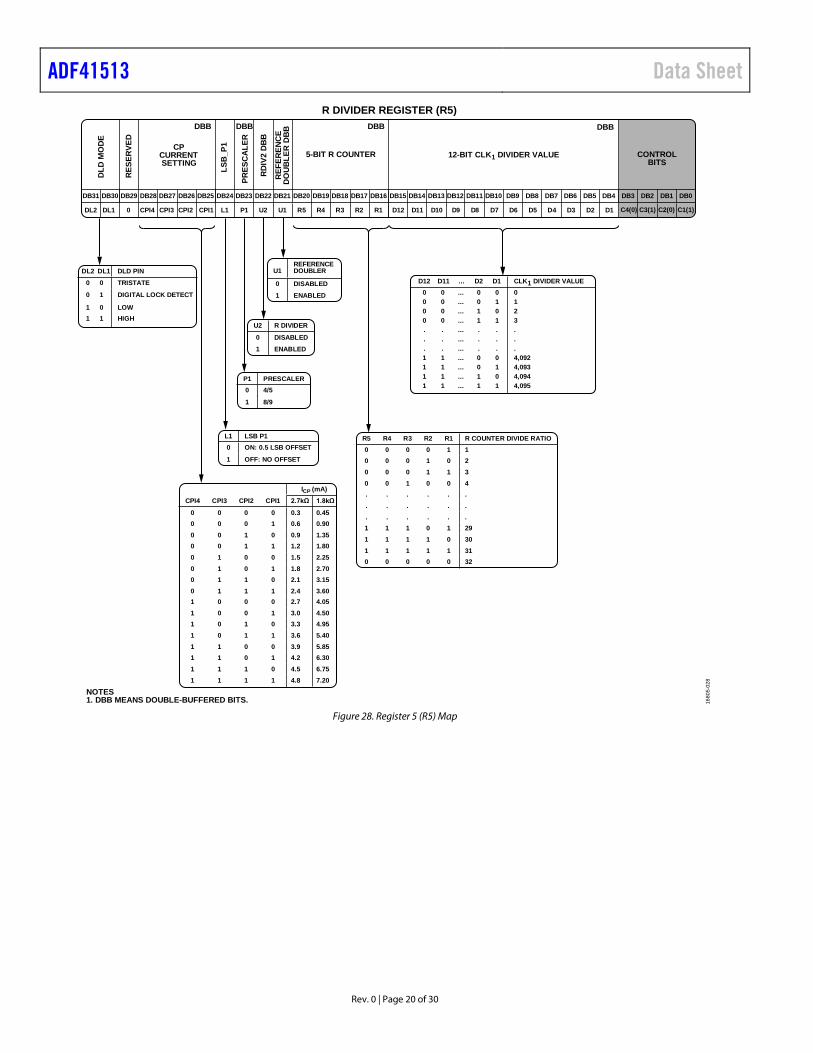
REGISTER 5 (R5) MAP DLD Modes
Register 5, Bits[31:30] set the digital lock detect (DLD) pin state. For normal digital lock detect, set Register 5, Bits[31:30] = 0b01. Other options tristate the pin and force a high or low logic level, as shown in Figure 28.
CP Current Setting
Register 5, Bits[28:25] set the charge pump current. Set these bits to the charge pump current that the loop filter is designed for based on the application of the user. The recommended practice is to design the loop filter for a charge pump current of 2.4 mA or 2.7 mA and then use the programmable charge pump current to fine tune the loop filter frequency response.
LSB_P1
Register 5, Bit 24 = 0 enables a 26th bit in the fixed modulus MOD value. Enabling the 26th bit reduces fractional spurs but the reduction also adds a fixed fPFD/226 frequency offset to the output frequency. To disable this frequency offset, set Register 5, Bit 24 = 1.
Prescaler
The dual modulus prescaler (4/5 and 8/9) is set by Register 5, Bit 23. The prescaler, at the input to the N divider, divides down
the fRFIN signal so that the N divider can operate correctly. The prescaler is based on a synchronous 4/5 core. The prescaler setting affects the RF frequency and the minimum and maximum INT value as follows:
For Integer N mode,
• Prescaler 4/5: 20 ≤ INT ≤ 511, fRFIN_MAX = 16 GHz • Prescaler 8/9: 64 ≤ INT ≤ 1023, fRFIN_MAX = 26.5 GHz
For fractional-N mode,
• Prescaler 4/5: 23 ≤ INT ≤ 511, fRFIN_MAX = 16 GHz • Prescaler 8/9: 75 ≤ INT ≤ 1023, fRFIN_MAX = 26.5 GHz
RDIV2
Register 5, Bit 22 controls the reference divide by 2 block. See the N Divider and R Counter section for more information. This feature can provide a 50% duty cycle signal to the PFD.
Reference Doubler
Register 5, Bit 21 controls the reference doubler block. See the N Divider and R Counter section for more information.
R Counter
Register 5, Bits[20:16] control the R counter value. See the N Divider and R Counter section for more information.
CLK1 Divider
Register 5, Bits[15:4] control the CLK1 divider value. See the Phase Resync section for more information.
MOD2 REGISTER (R4)
NOTES1. DBB MEANS DOUBLE-BUFFERED BITS.
DBB
CONTROLBITS24-BIT MOD2 VALUE (MOD2)
000 M1M2M3M4M5M6M8 M7M9M10M11M12M13M14M15M16M17M18M19M20M21M22M23M240
RES
ERVE
D
M24 M23 ... M2 M1 MOD2 WORD0 0 ... 0 0 00 0 ... 0 1 10 0 ... 1 0 20 0 ... 1 1 3. . ... . . .. . ... . . .. . ... . . .1 1 ... 0 0 16,777,2121 1 ... 0 1 16,777,2131 1 ... 1 0 16,777,2141 1 ... 1 1 16,777,215
DB31 DB30 DB29 DB28 DB27 DB26 DB25 DB24 DB23 DB22 DB21 DB20 DB19 DB18 DB17 DB16 DB15 DB14 DB13 DB12 DB11 DB10 DB9 DB8 DB7 DB6 DB5 DB4 DB3 DB2 DB1 DB0
C3(1)C4(0) C2(0) C1(0)
1680
5-02
7
Figure 27. Register 4 (R4) Map
ADF41513 Data Sheet
Rev. 0 | Page 20 of 30
5-BIT R COUNTER
LSB
_P1
PRES
CA
LER
RES
ERVE
D
DLD
MO
DE
RD
IV2
DB
B
DL2 DL1 0 CPI4 CPI3 CPI2 CPI1 P1 U2 U1 R5 R4 R3 R2 R1 D12 D11 D10 D9 D8 D7 D6 D5 D4 D3 D2 D1
R DIVIDER REGISTER (R5)DBB DBB DBB DBB
CONTROLBITS
12-BIT CLK1 DIVIDER VALUECP
CURRENTSETTING
REF
EREN
CE
DO
UB
LER
DB
B
L1
NOTES1. DBB MEANS DOUBLE-BUFFERED BITS.
U1REFERENCEDOUBLER
0 DISABLED
1 ENABLED
R5 R4 R3 R2 R1 R COUNTER DIVIDE RATIO0 0 0 0 1 10 0 0 1 0 20 0 0 1 1 30 0 1 0 0 4. . . . .. . . . .. . . . .
.
.
.1 1 1 0 1 291 1 1 1 0 301 1 1 1 1 310 0 0 0 0 32
U2 R DIVIDER
0 DISABLED
1 ENABLED
P1 PRESCALER0 4/5
1 8/9
DL1 DLD PIN
00 TRISTATE
1
DL2
10 DIGITAL LOCK DETECT
01 LOW1 HIGH
ICP (mA)
CPI4 CPI3 CPI2 CPI1 2.7kΩ
0 0 0 0 0.30 0 0 1 0.60 0 1 0 0.90 0 1 1 1.20 1 0 0 1.50 1 0 1 1.80 1 1 0 2.10 1 1 1 2.41 0 0 0 2.71 0 0 1 3.01 0 1 0 3.31 0 1 1 3.61 1 0 0 3.91 1 0 1 4.21 1 1 0 4.51 1 1 1 4.8
1.8kΩ
0.450.901.351.802.252.703.153.604.054.504.955.405.856.306.757.20
L1 LSB P10 ON: 0.5 LSB OFFSET
1 OFF: NO OFFSET
D12 D11 ... D2 D10000...1111
0000...1111
...
...
...
...
...
...
...
...
...
...
...
0011...0011
0101...0101
0123...4,0924,0934,0944,095
CLK1 DIVIDER VALUE
DB31 DB30 DB29 DB28 DB27 DB26 DB25 DB24 DB23 DB22 DB21 DB20 DB19 DB18 DB17 DB16 DB15 DB14 DB13 DB12 DB11 DB10 DB9 DB8 DB7 DB6 DB5 DB4 DB3 DB2 DB1 DB0
C3(1)C4(0) C2(0) C1(1)
1680
5-02
8
Figure 28. Register 5 (R5) Map
Data Sheet ADF41513
Rev. 0 | Page 21 of 30
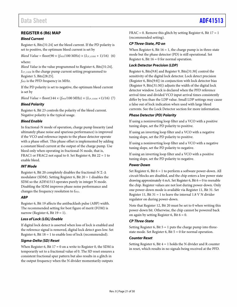
REGISTER 6 (R6) MAP Bleed Current
Register 6, Bits[31:24] set the bleed current. If the PD polarity is set to positive, the optimum bleed current is set by
Bleed Value = floor(90 × (fPFD/100 MHz) × (ICP_CODE + 1)/16) (6)
where: Bleed Value is the value programmed to Register 6, Bits[31:24]. ICP_CODE is the charge pump current setting programmed to Register 5, Bits[28:25]. fPFD is the PFD frequency in MHz.
If the PD polarity is set to negative, the optimum bleed current is set by
Bleed Value = floor(144 × (fPFD/100 MHz) × (ICP_CODE +1)/16) (7)
Bleed Polarity
Register 6, Bit 23 controls the polarity of the bleed current. Negative polarity is the typical usage.
Bleed Enable
In fractional-N mode of operation, charge pump linearity (and ultimately phase noise and spurious performance) is improved if the VCO and reference inputs to the phase detector operate with a phase offset. This phase offset is implemented by adding a constant bleed current at the output of the charge pump. Use bleed only when operating in fractional-N mode, that is, FRAC1 or FRAC2 not equal to 0. Set Register 6, Bit 22 = 1 to enable bleed.
INT Mode
Register 6, Bit 20 completely disables the fractional-N Σ-Δ modulator (SDM). Setting Register 6, Bit 20 = 1 disables the SDM so the ADF41513 operates purely in integer N mode. Disabling the SDM improves phase noise performance and changes the frequency resolution to fPFD.
ABP
Register 6, Bit 19 affects the antibacklash pulse (ABP) width. The recommended setting for best figure of merit (FOM) is narrow (Register 6, Bit 19 = 1).
Loss of Lock (LOL) Enable
If digital lock detect is asserted when loss of lock is enabled and the reference signal is removed, digital lock detect goes low. Set Register 6, Bit 18 = 1 to enable loss of lock (recommended).
Sigma-Delta (SD) Reset
When Register 6, Bit 17 = 0 on a write to Register 0, the SDM is temporarily set to a fractional value of 0. The SD reset ensures a consistent fractional spur pattern but also results in a glitch in the output frequency when the N divider momentarily outputs
FRAC = 0. Remove this glitch by setting Register 6, Bit 17 = 1 (recommended setting).
CP Three-State, PD on
When Register 6, Bit 16 = 1, the charge pump is in three-state mode but the phase detector (PD) is still operational. Set Register 6, Bit 16 = 0 for normal operation.
Lock Detector Precision (LDP)
Register 6, Bits[9:8] and Register 9, Bits[31:30] control the sensitivity of the digital lock detector. Lock detect precision (Register 6, Bits[9:8]) in conjunction with lock detector bias (Register 9, Bits[31:30]) adjusts the width of the digital lock detector window. Lock is declared when the PFD reference arrival time and divided VCO input arrival times consistently differ by less than the LDP value. Small LDP settings may cause a false out of lock indication when used with large bleed currents. See the Lock Detector section for more information.
Phase Detector (PD) Polarity
If using a noninverting loop filter and a VCO with a positive tuning slope, set the PD polarity to positive.
If using an inverting loop filter and a VCO with a negative tuning slope, set the PD polarity to positive.
If using a noninverting loop filter and a VCO with a negative tuning slope, set the PD polarity to negative.
If using an inverting loop filter and a VCO with a positive tuning slope, set the PD polarity to negative.
Power Down
Set Register 6, Bit 6 = 1 to perform a software power-down. All circuit blocks are disabled, and the chip enters a low power state drawing approximately 4 mA. Set Register 6, Bit 6 = 0 to reenable the chip. Register values are not lost during power-down. Only one power-down mode is available via Register 11, Bit 31. Set Register 11, Bit 31 = 1 to leave the internal 1.8 V N divider regulator on during power-down.
Note that Register 12, Bit 20 must be set to 0 when writing this power-down bit. Otherwise, the chip cannot be powered back on again by setting Register 6, Bit 6 = 0.
CP Three-State
Setting Register 6, Bit 5 = 1 puts the charge pump into three-state mode. Set Register 6, Bit 5 = 0 for normal operation.
Counter Reset
Setting Register 6, Bit 4 = 1 holds the N divider and R counter in reset, which results in no signals being received at the PFD.
ADF41513 Data Sheet
Rev. 0 | Page 22 of 30
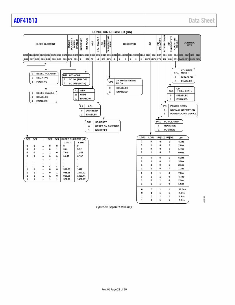
BLEED CURRENT
POW
ER D
OW
N
PDPO
LAR
ITY
LDP
CO
UN
TER
RES
ET
CP
THR
EE-S
TATE
BC7BC8 BC6 BC5 BC4 BC3 BC2 BC1 BP1 BE1 IM1 A1 L1 SR1 1 0 LDP1 PP1 PD C31 CR1
FUNCTION REGISTER (R6)
SDR
ESET
AB
P
INT
MO
DE
RESERVED
BLE
EDPO
LAR
ITY
BLE
EDEN
AB
LE
LOL
ENA
BLE
CONTROLBITS
PP1 PD POLARITY
0 NEGATIVE
1 POSITIVE
LDP2 LDP0 4.3ns
11.7ns
SR1 SD RESET
0 RESET ON R0 WRITE1 NO RESET
CR1COUNTERRESET
0 DISABLED1 ENABLED
C31CPTHREE-STATE
0 DISABLED1 ENABLED
L1 LOL
0 DISABLED1 ENABLED
0 BLEED POLARITY
0 NEGATIVE
1 POSITIVE
0 BLEED ENABLE
0 DISABLED
1 ENABLED
A1 ABP
0 WIDE
1 NARROW
IM1 INT MODE0 SD ON (FRAC-N)1 SD OFF (INT-N)
BC8 BC7 ... BC2 BC1 BLEED CURRENT (µA)
0 0 ... 0 0 00 0 ... 0 1 3.810 0 ... 1 0 7.630 0 ... 1 1 11.44. . ... . . .. . ... . . .. . ... . . .1 1 ... 0 0 961.331 1 ... 0 1 965.151 1 ... 1 0 968.961 1 ... 1 1 972.78
05.7211.4417.17...14421447.721453.441459.17
0 0 0 0 LDP2
LDP1
001 0
11
2.8ns
0.9ns
0
RES
ERVE
D
CP
THR
EE-S
TATE
PD O
N
R9[31] R9[30]
0 00 00 00 0
5.2ns
2.1ns3.5ns
1.2ns
7.0ns
2.9ns4.7ns
1.6ns
11.5ns
4.9ns7.9ns
2.8ns
010
01 0
11
010
01 0
11
010
01 0
11
0 10 10 10 1
1 01 01 01 0
1 11 11 11 1
CP1
CP1 CP THREE-STATEPD ON
0 DISABLED1 ENABLED
POWER DOWN
NORMAL OPERATION
PD
01 POWER-DOWN DEVICE
DB31 DB30 DB29 DB28 DB27 DB26 DB25 DB24 DB23 DB22 DB21 DB20 DB19 DB18 DB17 DB16 DB15 DB14 DB13 DB12 DB11 DB10 DB9 DB8 DB7 DB6 DB5 DB4 DB3 DB2 DB1 DB0
C3(1)C4(0) C2(1) C1(0)
1680
5-02
9
2.7kΩ 1.8kΩ
Figure 29. Register 6 (R6) Map
Data Sheet ADF41513
Rev. 0 | Page 23 of 30
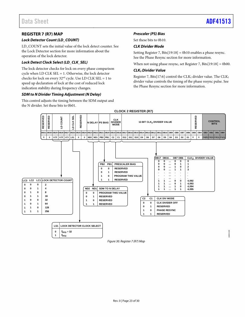
REGISTER 7 (R7) MAP Lock Detector Count (LD_COUNT)
LD_COUNT sets the initial value of the lock detect counter. See the Lock Detector section for more information about the operation of the lock detector.
Lock Detect Clock Select (LD_CLK_SEL)
The lock detector checks for lock on every phase comparison cycle when LD CLK SEL = 1. Otherwise, the lock detector checks for lock on every 32nd cycle. Use LD CLK SEL = 1 to speed up declaration of lock at the cost of reduced lock indication stability during frequency changes.
SDM to N Divider Timing Adjustment (N Delay)
This control adjusts the timing between the SDM output and the N divider. Set these bits to 0b01.
Prescaler (PS) Bias
Set these bits to 0b10.
CLK Divider Mode
Setting Register 7, Bits[19:18] = 0b10 enables a phase resync. See the Phase Resync section for more information.
When not using phase resync, set Register 7, Bits[19:18] = 0b00.
CLK2 Divider Value
Register 7, Bits[17:6] control the CLK2 divider value. The CLK2 divider value controls the timing of the phase resync pulse. See the Phase Resync section for more information.
CLOCK 2 REGISTER (R7)
12-BIT CLK2 DIVIDER VALUE
0 LC3 LC2 LC1 LS1 0 0 ND2 ND1 PB2 PB1 C2 C1 D12 D11 D10 D9 D8 D7 D6 D5 D4 D3 D2 D1
CLKDIVIDERMODE
CONTROLBITS
RES
ERVE
D
DB17 DB16... DB7 DB60000...1111
0000...1111
...
...
...
...
...
...
...
...
...
...
...
0011...0011
0101...0101
0123...4,0924,0934,0944,095
CLK2 DIVIDER VALUE
C2 CLK DIV MODE
0 CLK DIVIDER OFF
1
C1
0
1 RESERVED1 0 PHASE RESYNC0 1 RESERVED
0
RES
ER
VED
0 0
LD C
LK S
EL
LD C
OU
NT
LC2 LOCK DETECTOR COUNT
0
1
LC1
0
11 00 1
LC3
0
000
0
1
0
11 00 1
1
111
248163264128256
LOCK DETECTOR CLOCK SELECT
fPFD ÷ 32
LS1
01 fPFD
PS BIASN DELAY
PB2 PRESCALER BIAS
0 RESERVED
1
PB1
0
1 RESERVED1 0
RESERVED0 1PROGRAM THIS VALUE
ND2 SDM TO N DELAY
0 PROGRAM THIS VALUE
1
ND1
0
1 RESERVED1 0 RESERVED0 1 RESERVED
RES
ER
VED
RES
ERVE
D
DB31 DB30 DB29 DB28 DB27 DB26 DB25 DB24 DB23 DB22 DB21 DB20 DB19 DB18 DB17 DB16 DB15 DB14 DB13 DB12 DB11 DB10 DB9 DB8 DB7 DB6 DB5 DB4 DB3 DB2 DB1 DB0
C3(1)C4(0) C2(1) C1(1)
1680
5-03
0
Figure 30. Register 7 (R7) Map
ADF41513 Data Sheet
Rev. 0 | Page 24 of 30
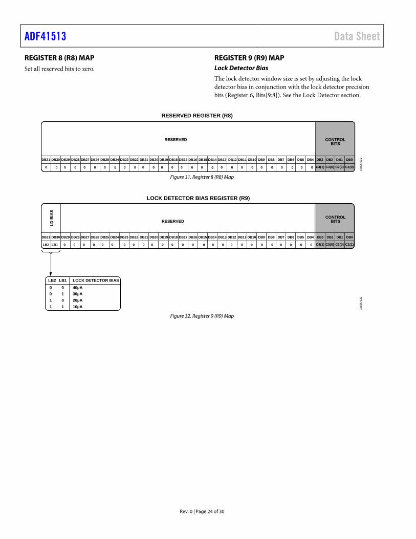
REGISTER 8 (R8) MAP Set all reserved bits to zero.
REGISTER 9 (R9) MAP Lock Detector Bias
The lock detector window size is set by adjusting the lock detector bias in conjunction with the lock detector precision bits (Register 6, Bits[9:8]). See the Lock Detector section.
0
RESERVED REGISTER (R8)
RESERVED CONTROLBITS
000 000000 0000 000000 0000 0000
DB31 DB30 DB29 DB28 DB27 DB26 DB25 DB24 DB23 DB22 DB21 DB20 DB19 DB18 DB17 DB16 DB15 DB14 DB13 DB12 DB11 DB10 DB9 DB8 DB7 DB6 DB5 DB4 DB3 DB2 DB1 DB0
C3(0)C4(1) C2(0) C1(0)
1680
5-03
1
Figure 31. Register 8 (R8) Map
LB1
LOCK DETECTOR BIAS REGISTER (R9)
RESERVEDCONTROL
BITS
0 0 0 0 0 0 0 0 0 0 0 0 0 0 0 0 0 0 0 0 0 0 0 0 0 0LB2
LB2 LOCK DETECTOR BIAS
0 40µA
1
LB1
0
1 10µA1 0 20µA0 1 30µA
LD B
IAS
DB31 DB30 DB29 DB28 DB27 DB26 DB25 DB24 DB23 DB22 DB21 DB20 DB19 DB18 DB17 DB16 DB15 DB14 DB13 DB12 DB11 DB10 DB9 DB8 DB7 DB6 DB5 DB4 DB3 DB2 DB1 DB0
C3(0)C4(1) C2(0) C1(1)
1680
5-03
2
Figure 32. Register 9 (R9) Map
Data Sheet ADF41513
Rev. 0 | Page 25 of 30
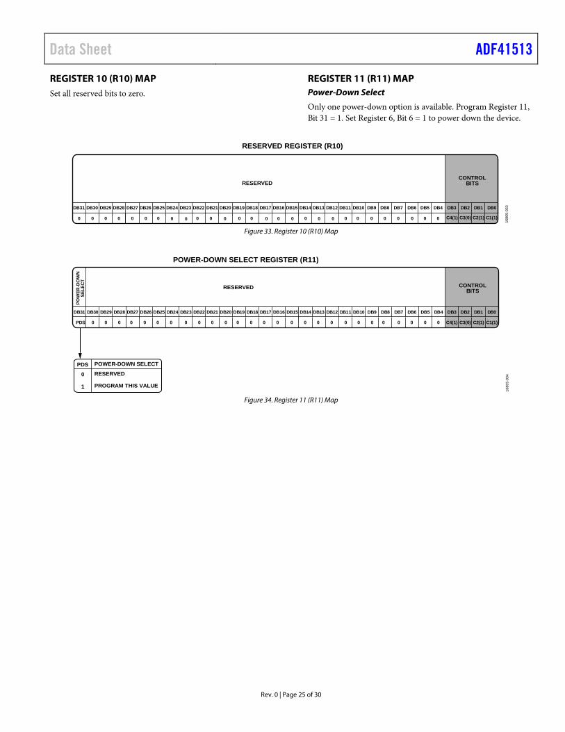
REGISTER 10 (R10) MAP Set all reserved bits to zero.
REGISTER 11 (R11) MAP Power-Down Select
Only one power-down option is available. Program Register 11, Bit 31 = 1. Set Register 6, Bit 6 = 1 to power down the device.
RESERVED
0 0 0 0 0 0 0 0
RESERVED REGISTER (R10)
CONTROLBITS
000000000000000000 00
DB31 DB30 DB29 DB28 DB27 DB26 DB25 DB24 DB23 DB22 DB21 DB20 DB19 DB18 DB17 DB16 DB15 DB14 DB13 DB12 DB11 DB10 DB9 DB8 DB7 DB6 DB5 DB4 DB3 DB2 DB1 DB0
C3(0)C4(1) C2(1) C1(1)
1680
5-03
3
Figure 33. Register 10 (R10) Map
DB31 DB30 DB29 DB28 DB27 DB26 DB25 DB24 DB23 DB22 DB21 DB20 DB19 DB18 DB17 DB16 DB15 DB14 DB13 DB12 DB11 DB10 DB9 DB8 DB7 DB6 DB5 DB4 DB3 DB2 DB1 DB0
PDS 0 0 0 CC4(1) 3(0) C2(1) C1(1)
POWER-DOWN SELECT REGISTER (R11)
RESERVED CONTROLBITS
0 0 0 0 0 0 0 0 0 0 00 0 0 0 00 0 0 0 0 0 0 0
PDS POWER-DOWN SELECT
0 RESERVED
1 PROGRAM THIS VALUE
1680
5-03
4
POW
ER-D
OW
NSE
LECT
Figure 34. Register 11 (R11) Map
ADF41513 Data Sheet
Rev. 0 | Page 26 of 30
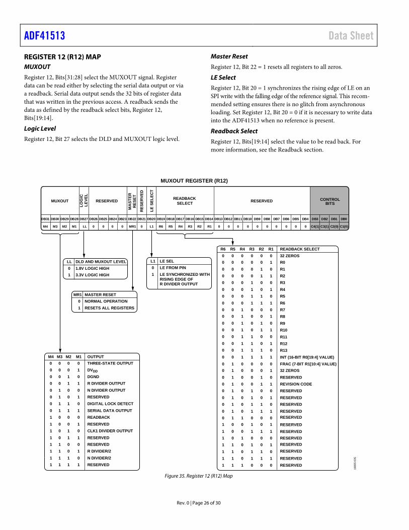
REGISTER 12 (R12) MAP MUXOUT
Register 12, Bits[31:28] select the MUXOUT signal. Register data can be read either by selecting the serial data output or via a readback. Serial data output sends the 32 bits of register data that was written in the previous access. A readback sends the data as defined by the readback select bits, Register 12, Bits[19:14].
Logic Level
Register 12, Bit 27 selects the DLD and MUXOUT logic level.
Master Reset
Register 12, Bit 22 = 1 resets all registers to all zeros.
LE Select
Register 12, Bit 20 = 1 synchronizes the rising edge of LE on an SPI write with the falling edge of the reference signal. This recom-mended setting ensures there is no glitch from asynchronous loading. Set Register 12, Bit 20 = 0 if it is necessary to write data into the ADF41513 when no reference is present.
Readback Select
Register 12, Bits[19:14] select the value to be read back. For more information, see the Readback section.
DB31
RESERVED
MA
STER
RES
ET
LE S
ELEC
T
DB30 DB29 DB28 DB27 DB26 DB25 DB24 DB23 DB22 DB21 DB20 DB19 DB18 DB17 DB16 DB15 DB14 DB13 DB12 DB11 DB10 DB9 DB8 DB7 DB6 DB5 DB4 DB3 DB2 DB1 DB0
M4 M3 M2 M1 0 0000LL MR1 L1 R6 R5 R4 R3 R2 R1 0 0 0 0 0 0 0 0 0 0 CC4(1) 3(1) C2(0) C1(0)
MUXOUT REGISTER (R12)
MUXOUT RESERVED
RES
ERVE
D
READBACKSELECT
CONTROLBITS
M4 M3 M2 M1 OUTPUT0 0 0 0 THREE-STATE OUTPUT0 0 0 1 DVDD0 0 1 0 DGND0 0 1 1 R DIVIDER OUTPUT0 1 0 0 N DIVIDER OUTPUT0 1 0 1 RESERVED0 1 1 0 DIGITAL LOCK DETECT0 1 1 1 SERIAL DATA OUTPUT1 0 0 0 READBACK1 0 0 1 RESERVED1 0 1 0 CLK1 DIVIDER OUTPUT1 0 1 1 RESERVED1 1 0 0 RESERVED1 1 0 1 R DIVIDER/21 1 1 0 N DIVIDER/21 1 1 1 RESERVED
R6 R5 R4 R3 R2 R1 READBACK SELECT0 0 0 0 0 00 0 0 0 0 10 0 0 0 1 00 0 0 0 1 10 0 0 1 0 00 0 0 1 0 10 0 0 1 1 00 0 0 1 1 10 0 1 0 0 00 0 1 0 0 10 0 1 0 1 00 0 1 0 1 10 0 1 1 0 00 0 1 1 0 10 0 1 1 1 00 0 1 1 1 1
32 ZEROSR0R1R2R3R4R5R6R7R8R9R10R11R12R13INT (16-BIT R0[19:4] VALUE)
0 1 0 0 0 00 1 0 0 0 10 1 0 0 1 00 1 0 0 1 10 1 0 1 0 00 1 0 1 0 10 1 0 1 1 00 1 0 1 1 10 1 1 0 0 01 0 0 1 0 11 0 0 1 1 11 0 1 0 0 01 1 0 1 0 11 1 0 1 1 01 1 0 1 1 11 1 1 0 0 0
FRAC (7-BIT R1[10:4] VALUE)32 ZEROSRESERVEDREVISION CODE
MR1 MASTER RESET0 NORMAL OPERATION
RESETS ALL REGISTERS1
L1 LE SEL0 LE FROM PIN
LE SYNCHRONIZED WITHRISING EDGE OFR DIVIDER OUTPUT
1
LL DLD AND MUXOUT LEVEL0 1.8V LOGIC HIGH
3.3V LOGIC HIGH1
LOG
IC L
EVEL
RESERVEDRESERVEDRESERVEDRESERVEDRESERVED
RESERVEDRESERVEDRESERVEDRESERVEDRESERVED
RESERVEDRESERVED
1680
5-03
5
Figure 35. Register 12 (R12) Map
Data Sheet ADF41513
Rev. 0 | Page 27 of 30
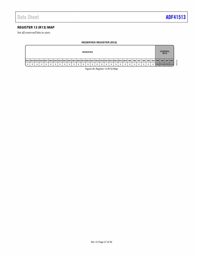
REGISTER 13 (R13) MAP Set all reserved bits to zero.
RESERVED
0 0 00000 0 0 000000000 0 0 0 0 0 0 0 0 0 0
RESERVED REGISTER (R13)
CONTROLBITS
DB31 DB30 DB29 DB28 DB27 DB26 DB25 DB24 DB23 DB22 DB21 DB20 DB19 DB18 DB17 DB16 DB15 DB14 DB13 DB12 DB11 DB10 DB9 DB8 DB7 DB6 DB5 DB4 DB3 DB2 DB1 DB0
C3(1)C4(1) C2(0) C1(1)
1680
5-03
6
Figure 36. Register 13 (R13) Map
ADF41513 Data Sheet
Rev. 0 | Page 28 of 30
APPLICATIONS INFORMATION INITIALIZATION SEQUENCE The following sequence of registers is the correct sequence for initial power-up of the ADF41513 after the correct application of voltages to the supply pins:
1. Register 13 2. Register 12 3. Register 11 4. Register 10 5. Register 9 6. Register 8 7. Register 7 8. Register 6 9. Register 5 10. Register 4 11. Register 3 12. Register 2 13. Register 1 14. Register 0
RF SYNTHESIZER: A WORKED EXAMPLE OF 25-BIT FIXED MODULUS MODE The following equation governs how to program the synthesizer:
RFOUT = (INT + (FRAC1/225)) × fPFD (7)
where: RFOUT is the RF frequency output. INT is the integer division factor. FRAC1 is the fractional numerator. fPFD is the PFD frequency.
For example, in a system where a 12.102 GHz RF frequency output (RFOUT) is required and a 100 MHz reference frequency input (REFIN) is available, the frequency resolution, fRES, is
fRES = REFIN/225
fRES = 100 MHz/225
= 2.98 Hz
From Equation 1 and Equation 2,
fPFD = (100 MHz × (1 + 0)/1) = 100 MHz 12.102 GHz = 100 MHz × (N + FRAC/225)
Calculating the INT and FRAC values,
INT = int(RFOUT/fPFD) = 121
FRAC1 = (int(RFOUT/fPFD) − INT) × 225 = 671088.64 ≈ 671089
where: INT is the 16-bit INT value in Register 0. FRAC1 is the 25-bit FRAC1 value in Register 1. int() makes an integer of the argument in parentheses.
Note that 671088.64 is rounded to 671,089, resulting in a small frequency error. For exact frequency, use the variable modulus mode.
RF SYNTHESIZER: A WORKED EXAMPLE OF VARIABLE MODULUS MODE The following is an example how to program the ADF41513 synthesizer:
RFOUT = fPFD × (INT + (FRAC1 + (FRAC2/MOD2))/225) (8)
where: RFOUT is the output frequency of the external VCO. INT is a 16-bit value set by Bits[19:4] in Register 0. In Integer N mode, INT is 20 to 511 for a 4/5 prescaler and 64 to 1023 for a 8/9 prescaler, and in fractional-N mode, INT is 23 to 511 for a 4/5 prescaler and 75 to 1023 for a 8/9 prescaler. FRAC1 is a 25-bit value set by Bits[28:4] in Register 1. FRAC2 is a 24-bit value set by Bits[27:4] in Register 3. MOD2 is a 24-bit value set by Bits[27:4] in Register 4. fPFD is the PFD frequency.
For example, in a system where a 12.102 GHz RFOUT is required and a 100 MHz fPFD is available,
INT = int(RFOUT/fPFD) = 121 FRAC1 = int(((RFOUT/fPFD) – INT) × 225) = 671,088
where: int() makes an integer of the argument in parentheses.
Remainder = FRAC2/MOD2 = 0.64
where: FRAC2 = 64. MOD2 = 100.
MODULUS The choice of modulus (MOD) depends on the reference signal (REFIN) available and the channel resolution (fRES) required at the RF output.
REFERENCE DOUBLER AND REFERENCE DIVIDER The on-chip reference doubler allows the input reference signal to be doubled. Doubling is useful for increasing the PFD comparison frequency. Setting the PFD frequency higher improves the noise performance of the system. Doubling the PFD frequency usually improves noise performance by 3 dB. It is important to note that the reference input cannot operate above 225 MHz when the reference doubler is on. The PFD maximum operating frequency is 250 MHz (integer N mode) or 125 MHz (fractional-N mode) due to a limitation in the speed of the Σ-Δ circuit.
The reference divide by 2 divides the reference signal by 2, resulting in a 50% duty cycle PFD frequency.
Data Sheet ADF41513
Rev. 0 | Page 29 of 30
SPUR MECHANISMS This section describes the two different spur mechanisms that arise with a PLL, and how to minimize them in the ADF41513.
Integer Boundary Spurs
Interactions between the RF VCO frequency and the reference frequency cause integer boundary spurs. When these frequencies are not integer related (the point of a fractional-N synthesizer), spur sidebands appear on the VCO output spectrum at an offset frequency that corresponds to the beat note or difference frequency between an integer multiple of the reference and the VCO frequency. These spurs are attenuated by the loop filter and are more noticeable on channels close to integer multiples of the reference where the difference frequency can be inside the loop bandwidth.
Reference Spurs
Reference spurs are generally not a problem in fractional-N synthesizers because the reference offset is far outside the loop bandwidth. However, any reference feedthrough mechanism that bypasses the loop can cause a problem. Feedthrough of low levels of on-chip reference switching noise, through the RFINA pin or the RFINB pin back to the VCO, can result in reference spur levels as high as −90 dBc. PCB layout must ensure adequate isolation between VCO traces and the input reference to avoid a possible feedthrough path on the board.
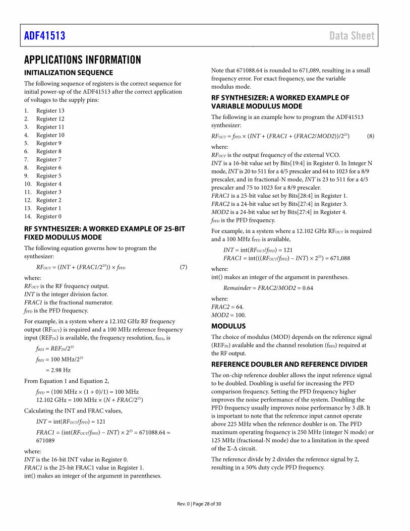
PHASE RESYNC The output of a 25-bit fractional-N PLL can settle to any of the 225 phase offsets with respect to the input reference. The phase resync feature in the ADF41513 produces a consistent output phase offset with respect to the input reference. This consistent output phase offset with respect to the input reference is neces-sary in applications where the output phase and frequency are important, such as digital beamforming. See the Phase Programmability section to program a specific RF output phase when using phase resync.
Phase resync is enabled by setting Register 7, Bits[19:18] = 0b10. When phase resync is enabled, an internal timer generates sync signals at intervals of tSYNC given by the following formula:
tSYNC = CLK1 × CLK2 × tPFD (9)
where: CLK1 is the decimal value programmed in Register 5, Bits[15:4]. CLK2 is the decimal value programmed in Register 7, Bits[17:6]. tPFD is the PFD reference period (1/fPFD).
When a new frequency is programmed, the second sync pulse after the LE rising edge resynchronizes the output phase to the reference. Program the tSYNC time to a value that is at least as long as the worst case lock time to guarantee that the phase resync occurs after the last cycle slip in the PLL settling transient.
In the example shown in Figure 37, tSYNC is set to 550 µs. The second sync pulse and any later sync pulses are ignored.
LE
PHASE
FREQUENCY
SYNC(INTERNAL)
–100 0 100 200 1000300 400 500 600 700 800 900TIME (µs)
PLL SETTLES TOCORRECT PHASEAFTER RESYNC
LAST CYCLE SLIP
PLL SETTLES TOINCORRECT PHASE
1680
5-03
7
Figure 37. Phase Resync Example
Phase Programmability
The phase word in Register 2 controls the RF output phase. As this word is changed from 0 to 212, the RF output phase changes over a 360° range in steps of phase value × 360°/212.
ADF41513 Data Sheet
Rev. 0 | Page 30 of 30
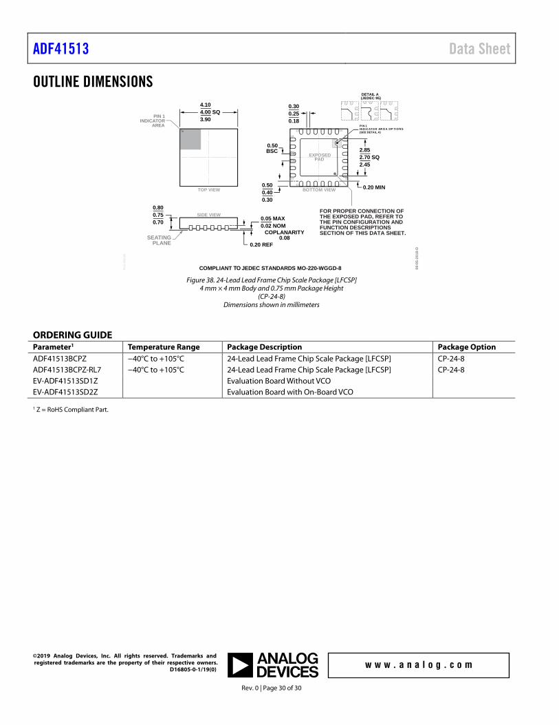
OUTLINE DIMENSIONS
0.50BSC
0.500.400.30
COMPLIANT TO JEDEC STANDARDS MO-220-WGGD-8
BOTTOM VIEWTOP VIEW
SIDE VIEW
4.104.00 SQ3.90
0.800.750.70 0.05 MAX
0.02 NOM
0.20 REF
COPLANARITY0.08
1
24
712
13
18
19
6
0.300.250.18
0.20 MIN
2.852.70 SQ2.45
EXPOSEDPAD
PKG
-005
185
09-0
5-20
18-D
P IN 1IN D ICATO R AR E A OP TIO N S(SEE DETAIL A)
DETAIL A(JEDEC 95)
FOR PROPER CONNECTION OFTHE EXPOSED PAD, REFER TOTHE PIN CONFIGURATION ANDFUNCTION DESCRIPTIONSSECTION OF THIS DATA SHEET.
SEATINGPLANE
PIN 1INDICATOR
AREA
Figure 38. 24-Lead Lead Frame Chip Scale Package [LFCSP]
4 mm × 4 mm Body and 0.75 mm Package Height (CP-24-8)
Dimensions shown in millimeters
ORDERING GUIDE Parameter1 Temperature Range Package Description Package Option ADF41513BCPZ −40°C to +105°C 24-Lead Lead Frame Chip Scale Package [LFCSP] CP-24-8 ADF41513BCPZ-RL7 −40°C to +105°C 24-Lead Lead Frame Chip Scale Package [LFCSP] CP-24-8 EV-ADF41513SD1Z Evaluation Board Without VCO EV-ADF41513SD2Z Evaluation Board with On-Board VCO 1 Z = RoHS Compliant Part.
©2019 Analog Devices, Inc. All rights reserved. Trademarks and registered trademarks are the property of their respective owners. D16805-0-1/19(0)