2015 results and 2017 inemi roadmap preview of selected iot,...
TRANSCRIPT

2015 Results and 2017 iNEMI Roadmap Preview of Selected IoT, Board Assembly & Optoelectronics Chapter Highlights
Speaker: Chuck Richardson, iNEMISMTAI2016September27,2016RosemontConventionCenterRosemont,IL

Topicsn iNEMI Introductionn iNEMI Roadmap Process Overviewn Situation Analysisn Technology Needsn Strategic Concernsn Paradigm Shiftsn IoT/Wearables Product Emulator Issuesn Board Assembly TWG Issuesn Optoelectronic TWG Issuesn Summary/Next Steps
2
About iNEMI
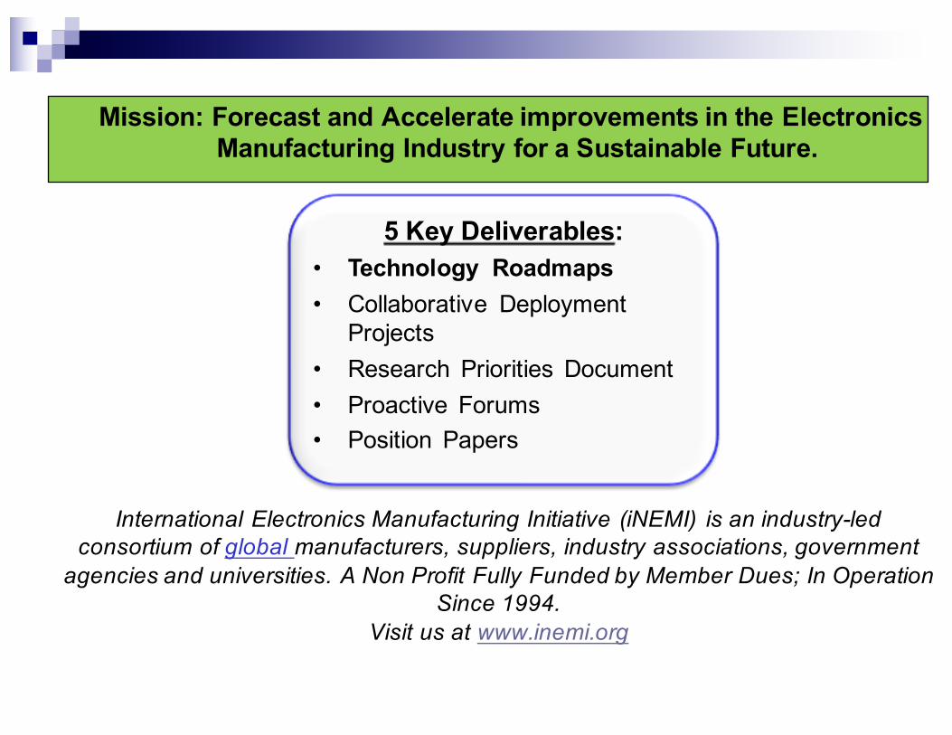
International Electronics Manufacturing Initiative (iNEMI) is an industry-led consortium of global manufacturers, suppliers, industry associations, government
agencies and universities. A Non Profit Fully Funded by Member Dues; In Operation Since 1994.
Visit us at www.inemi.org
5 Key Deliverables:• Technology Roadmaps• Collaborative Deployment
Projects• Research Priorities Document• Proactive Forums• Position Papers
Mission: Forecast and Accelerate improvements in the Electronics Manufacturing Industry for a Sustainable Future.

Roadmap Process & Scope

2015 Product Emulator Groups (PEGs)
Emulator Characteristics
Portable/WirelessProduced in high volumes, cost is the primary driver, hand held battery powered products are also driven by size and weight reduction
Consumer/Office Driven by the need for maximum performance over a wide range of cost targets
Automotive Products Products that must operate in an automotive environment
High-End Systems (The Cloud)
Products that serve the high performance computing/storage markets including networking, datacom and telecom and cover a wide range of cost and performance targets
Medical Products Products that must operate with high reliability and, in some cases, support life critical applications
5

2015 Technology Working Groups (TWGs)
Organic PCB InterconnectAssembly Customer
RF Components & Subsystems
OptoelectronicsLarge Area, Flexible Electronics
Energy Storage Systems
Modeling, Simulation, and Design
SemiconductorTechnology
Final Assembly
Mass Storage (Magnetic, Optical & Solid State)
Passive Components
Test, Inspection & Measurement
Environmentally Sustainable Electronics
Ceramic Substrates
Thermal Management
ElectronicConnectors
MEMS/Sensors
Green=Engineering Purple=Manufacturing Blue=Component & Subsystem
Solid State Illumination
Photovoltaics
Power Conversion Electronics

n > 500 participantsn > 280 companies/organizationsn 20 countries from 4 continentsn 19 Technology Working Groups (TWGs) n 5 Product Emulator Groups (PEGs)n ≈ 2000 pages of informationn Roadmaps the needs for 2015-2025
2015 Roadmap
7

Technical Plan for Members5 Year Plan for Implementation
2015 Technical
Plan
(iNEMI Members Only)
• Implementation Plan for Key Areas
• Key Gaps Prioritized by TC• Pre-competitive
Collaboration projects/plans developed by Members

2015 Research PrioritiesChapter 1: Introduction
Chapter 2: Research Needs to support iNEMI Technology Implementation Groups (TIGs) and current Projects
Chapter 3: Emerging Technologies
Chapter 4: Research Priorities Summarized by Research Area
DesignManufacturing ProcessesMaterials & ReliabilitySustainabilitySummary
Appendixes
2015ResearchPriorities
2015 iNEMI Roadmap Situation Analysis

Situation Analysis Examples: Technologyn Consumers’ demand for thin multifunctional products has led to
increased pressure on alternative high density packaging technologies.
n High-density 3D packaging has become the major technology challenge
n SiP:¨ Technology driver for small components, packaging,
assembly processes and for high density substratesn New sensors and MEMs:
¨ Expected to see exponential growth driven by portable products
¨ Motion gesture sensors expanding use of 2D-axis & 3D-axis gyroscopes
¨ Segment maturing, encouraging industry collaborationn 3D IC with TSV:
¨ Driven by Performance and Size requirements11

12
Technology Needs - Examplesn New MEMS/Sensors driven by Automotive, Medical,
IoT and Cell Phone applicationsn Thermal Management for Portable Productsn Development of viable rework process for Pb-free
solderingn Cooling Solutions for Portable Electronics (3D-TSV)n Reliability Evaluation and functional testing of MEMSn Testing of Energy Managed modulesn Functional Testing of Complex SIPsn Low Temperature Processingn Significant development will be required to drive down
the cost of batteries for EV (Electric Vehicle) applications from: $400/KWh to: $150/KWh.

Paradigm Shifts
n Need for continuous introduction of complex multifunctional products to address converging markets favors modular components or SiP (2-D & 3-D):¨ Increases flexibility¨ Shortens design cycle
n Cloud connected digital devices have the potential to enable major disruptions across the industry:¨ Major transition in business models¨ New Power Distribution Systems for Data Centers¨ Huge data centers operating more like utilities (selling data services)¨ Local compute and storage growth may slow (as data moves to the
cloud)¨ “Rent vs. buy” for software (monthly usage fee model)
n Rapid evolution and new challenges in energy consuming products such as SSL, Automotive and more
n Sensors everywhere – MEMS and wireless traffic!n “More Moore” (scaling of pitch) has reached its forecast limit and
must transition to heterogeneous integration - “More Than Moore”.13

Paradigm Shifts (continued)
n The Internet of Things (IoT) is making sensors ubiquitous; however, there are concerns about network security as cyber attacks become more pervasive.
n The focus in portables will shift to “wearables” with multiple sensors providing unique user interfaces and user interaction.
n Advancement of automotive safety systems and potentially broader use in other segments.

2017 iNEMI RoadmapPreview

2017 Product Emulator DescriptionsEmulator Characteristics
Wireless / PortableProduced in high volumes, cost is a primary driver, hand held battery powered products are also driven by features, size, weight reduction and battery life
Office / Consumer Systems Driven by the need for maximum performance and lowest cost
Automotive Products Products that must operate in an automotive environment
High-End Systems Products that serve the high end computing, networking, datacom and telecom markets and cover a wide range of cost and performance targets
Medical Products Products that must operate with high reliability and, in some cases, support life critical applications
Aerospace / Defense Products that must operate reliably in extreme environments
IoT / Wearables
Presently driven by a wide range of costs and capabilities. By adding internet connectivity and some intelligence to sensors/actuators, a wide range of applications including consumer and industrial product and process monitoring and control are made possible.
16
17
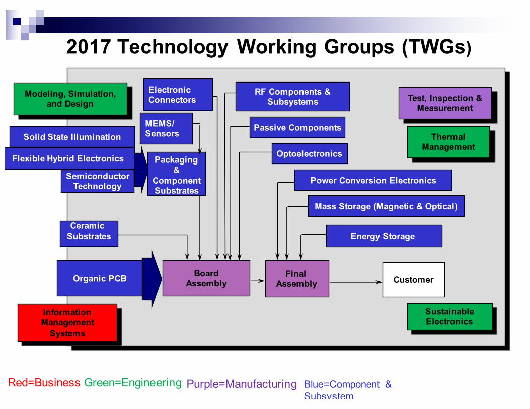
2017 Technology Working Groups (TWGs)
Organic PCB BoardAssembly Customer
RF Components & Subsystems
OptoelectronicsFlexible Hybrid Electronics
Energy Storage
Modeling, Simulation, and Design
Packaging &
Component Substrates
SemiconductorTechnology
Final Assembly
Mass Storage (Magnetic & Optical)
Passive Components
Information Management
Systems
Test, Inspection & Measurement
Sustainable Electronics
Ceramic Substrates
Thermal Management
Electronic Connectors
MEMS/Sensors
Red=Business Green=Engineering Purple=Manufacturing Blue=Component & Subsystem
Solid State Illumination
Power Conversion Electronics

Optoelectronics and Optical Storage
Organic Printed Circuit Boards
Magnetic and Optical Storage
Supply ChainManagement
Semiconductors
iNEMIInformation
ManagementTWG
iNEMIMass Data
Storage TWG
iNEMI / IPC / EIPC / TPCA
Organic PWBTWG
iNEMI / ITRS / MIG/PSMAPackaging
TWG
iNEMIBoard
Assembly TWG
Interconnect Substrates—Ceramic
iNEMI Roadmap
iNEMIOpto-
electronics TWG
Fifteen Contributing Organizations (2017)
iNEMI / MIG / ITRSMEMSTWG
iNEMIPassives
TWG
iNEMIHybrid Flexible
Electronics TWG

2017 Roadmap IoT/Wearables Product Sector Chapter Preview

IoT Situation Analysisn The Internet of Things is clearly a growing market.n Connected devices are used in a broad range of applicationsproviding entertainment, convenience, efficiency, and/or safetybenefits.n The market is also over-hyped, and figures are quoted withoutclear reference to definitions.n For suppliers of electronic hardware, it is often difficult tounderstand the impact of IoT on their businesses, and how best toposition their businesses to take advantage of the opportunitiesthat IoT presents.n iNEMI & Prismark define connected devices as devices thatconnect to the Internet directly or through a gateway.n Each device is also an independently deployable entity and caninitiate communications.
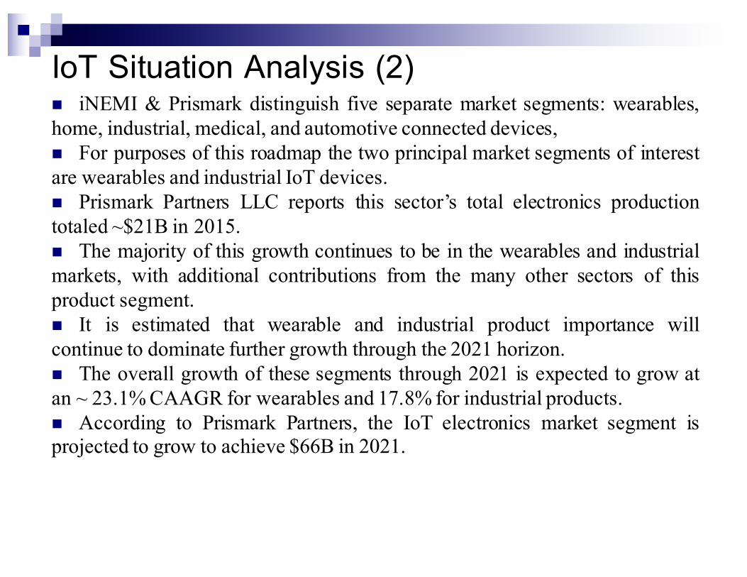
IoT Situation Analysis (2)n iNEMI & Prismark distinguish five separate market segments: wearables,home, industrial, medical, and automotive connected devices,n For purposes of this roadmap the two principal market segments of interestare wearables and industrial IoT devices.n Prismark Partners LLC reports this sector’s total electronics productiontotaled ~$21B in 2015.n The majority of this growth continues to be in the wearables and industrialmarkets, with additional contributions from the many other sectors of thisproduct segment.n It is estimated that wearable and industrial product importance willcontinue to dominate further growth through the 2021 horizon.n The overall growth of these segments through 2021 is expected to grow atan ~ 23.1% CAAGR for wearables and 17.8% for industrial products.n According to Prismark Partners, the IoT electronics market segment isprojected to grow to achieve $66B in 2021.

IoT/Wearables Market Growth Trend Forecast
IoT Product Forecast Growth (Source: Prismark Partners LLC)

IoT / Wearables Key Attribute Spreadsheet Example
n An important part of each PEG Chapter is their “key attributes spreadsheet” that lists a large number (more than 200) of key attributes expected to be needed for their product sector OEMs to be competitive over the ten year horizon covered by the roadmap.
n A sample of part of the IoT section on needs for industrial PCB Costs follows:

IoT PEG “Key Attributes” Example For PCB Needs
Parameter Descriptions Metric 2015 2017 2019 2021 2027
PCB Costs FR4 Unless Otherwise Stated 1 Layer Flexible State of the Art (production volume) $ per cm2 NA NA NA NA NA2 layer flexible State of the Art (production volume) $ per cm2 NA NA NA NA NA2 layer Rigid State of the Art (production volume) $ per cm2 NA NA NA NA NA3 layer flex State of the Art (production volume) $ per cm2 NA NA NA NA NA4 layer flexible State of the Art (production volume) $ per cm2 NA NA NA NA NA6 layer flex (with micro vias) State of the Art (production volume) $ per cm2 NA NA NA NA NA4 layer conventional State of the Art (production volume) $ per cm2 0.0140 0.0137 0.0134 0.0132 0.01164 layer - embedded capacitor / resistor High End $ per cm2 NA NA NA NA NA6 layer conventional State of the Art (production volume) $ per cm2 0.019 0.0182 0.0175 0.0168 0.01484 layer w/ microvia State of the Art (production volume) $ per cm2 NA NA NA NA NA6layer rigid (with micro vias) State of the Art (production volume) $ per cm2 0.0350 0.0315 0.0284 0.0255 0.01796 layer, blind/buried State of the Art (production volume) $ per cm2 NA NA NA NA NA6 layer - embedded capacitor / resistor High End $ per cm2 NA NA NA NA NA8 layer State of the Art (production volume) $ per cm2 0.0230 0.0221 0.0212 0.0203 0.01798 layer w/ microvias State of the Art (production volume) $ per cm2 0.0441 0.0397 0.0357 0.0321 0.02258 layer w/ blind/buried State of the Art (production volume) $ per cm2 NA NA NA NA NA8 layer colaminated (ALIVH) State of the Art (production volume) $ per cm2 NA NA NA NA NA10 layer conventional State of the Art (production volume) $ per cm2 0.0270 0.0259 0.0249 0.0239 0.021010 layer w/ microvias State of the Art (production volume) $ per cm2 0.0513 0.0462 0.0416 0.0374 0.026210 layer w/ blind / buried State of the Art (production volume) $ per cm2 NA NA NA NA NA10 layer colaminated (ALIVH) State of the Art (production volume) $ per cm2 NA NA NA NA NA12 layer Conventional (FR4) State of the Art (production volume) $ per cm2 0.031 0.0298 0.0286 0.0274 0.024112 layer conventional (FR4) with buried vias State of the Art (production volume) $ per cm2 NA NA NA NA NA12 layer conventional (FR4) with buried and m-vias State of the Art (production volume) $ per cm2 NA NA NA NA NA12 layer conventional (Aramid) State of the Art (production volume) $ per cm2 NA NA NA NA NA12 layer conventional (Aramid) with buried vias State of the Art (production volume) $ per cm2 NA NA NA NA NA12 layer conventional (Aramid) with buried and m-vias State of the Art (production volume) $ per cm2 NA NA NA NA NA14 layer, no blind/buried State of the Art (production volume) $ per cm2 0.035 0.0336 0.0323 0.0310 0.0272

2017 Roadmap Board Assembly TWG Chapter Preview

26
Content
vBoardAssembly§NPI,AssemblyMaterial§Press-Fit,Repairandrework§Wave/selectivesoldering
vExecutiveSummary

AssemblyMaterial(Chair:JenniferNguyen)
nAssemblyMaterial2017Roadmap¨ Updatingall material sections used in the second
level Board Assembly process.nSomeAreasofFocus/Trends
n Solder Paste¨ Lead-free continues to migrate into high reliable products (automotive, industrial,
medical, etc…)¨ Lead-free alloy alternatives for high reliable products (customer example)¨ Low process temperature than SAC305 with similar (or better) reliability
performance.n Solder Bar
¨ SAC 305 Alternatives, Low Agn Assembly Fluxes
¨ Halogen free, no halogen¨ Fluxes for higher temperature process¨ Fluxes to mitigate defects caused by component warpage such as HiP, NWO,
etc…n Underfill
¨ Low standoff height component (QFN/LGA)n Heat Sink Attach/ TIM
¨ Low cost, high performancen Die Attach Material
¨ Lead-Free¨ High Thermal

AssemblyMaterial(Chair:JenniferNguyen)
nSomeAreasofFocus/Trends(Cont’d)¨ Conformal Coating
n Low cost, but high performance for DC running in air with Sulfur and high T/RH
¨ Potting Materials n High powern Low pressure
¨ Other Encapsulants¨ Nano Materials
n Nano materials have been developed and more materials will be used in second level board assembly such as nano solder/adhesive, nano coating, etc...
¨ Will focus on issues/ gaps/challenges of these materials on 2017 roadmap.
nStatusUpdate¨ Kickoffteammeeting (05/26/16).¨ Willsend outsurveyforinputs¨ Target torelease initial draftinJuly/August.

Example – Preliminary Materials Section TableParameter Definition 2015 2017 2019 2021 2027
Solder Paste
Alloy
SAC/ SAC/ SAC/ SAC/ SAC/ Modified
SnCu/ Modified SnCu/ Modified SnCu/ Modified SnCu/
Modified SnCu/
Low Ag SAC Low Ag SAC Low Ag SAC Low Ag SAC Low Ag SAC Alloy (Low
Temp) Low Temp Low Temp Low Temp Low Temp Low Temp
Alloy (Lead-free) High Temp High Temp High Temp High Temp High Temp
High Temp>260C
Halogen-free
Zero Halogen
Bar Solder Alloy
SAC/ SAC/ SAC/ SAC/ SAC/ Modified
SnCu/ Modified SnCu/ Modified SnCu/ Modified SnCu/
Modified SnCu/
Low Ag SAC Low Ag SAC Low Ag SAC Low Ag SAC Low Ag SAC
Wave Solder Flux
VOC Free higher performance
Halogen free
Zero Halogen
Flux-cored Solder Wire
Alloy
SAC/ SAC/ SAC/ SAC/ SAC/ Modified
SnCu/ Modified SnCu/ Modified SnCu/ Modified SnCu/
Modified SnCu/
Low Ag SAC Low Ag SAC Low Ag SAC Low Ag SAC Low Ag SAC
Low Temp
Repair Fluxes
Repair Gel/Tacky Fluxes
Better performance,
higher reliability
Better performance,
higher reliability
Better performance,
higher reliability
Repair Liquid Fluxes
Better performance,
higher reliability
Better performance,
higher reliability
Better performance,
higher reliability
Die Attach Preforms
High Thermal conductivity
Matched CTE capability
Die Attach Adhesives
Lead-free compatibility JEDEC +260
reflow, small die, paste
JEDEC L1 @260
JEDEC L1 @260
JEDEC L1 @260
JEDEC L1 @260
JEDEC L1 @260
Lead-free compatibility JEDEC +260
reflow, large die, paste
JEDEC L1 @260
JEDEC L1 @260
JEDEC L1 @260
JEDEC L1 @260
JEDEC L1 @260

Press-Fit(Chair:DennisWillie)
nPress-fitforelectricalandmechanicalinterconnection¨ CrossCutwithTestandInspectionTWG
n Improvemethodstoinspectcompliantpintrueposition,absence andpresence¨ CrossCutwithConnectorTWG
n Reworkn DDR3&4contactinterconnect problemof>2000dpm atSFT
¨ Thefanaticofparticulate controlandmgmtduetoDIMMfalloutn HigherSignalintegrityrequirement askingfordifferent andadvancecontactmethodologybeyondcurrentpress-fit¨ Phase1-normalforceofbothcontacts>50gf,SItestpassed¨ PhaseII&III
EON (Eye of the Needle) Style Compliant Pin and Cross Sectional View within PCB. Press
Fit Connectors Installed on PCB
Rework and Repair Section (Chair: Jasbir Bath)
nUpdatinghandsoldering,PTHrework,areaarrayandnon-standardcomponentreworksectionsfrom2015roadmapinrelationtotin-leadandlead-freereworksolderingtechnologies.
nOneofthefocusareaswillbetounderstandifthereareanydevelopmentsforsolderingfluxmaterialsforrework.
nOtherareasoffocusincludeanynewdevelopmentsinthereworkofnew/emergingcomponentssuchasQFN/BTC/MLFandPoP components.
nGroupreviewingandupdatingsectionsincludeOEMs,EMS,solderingmaterialandreworkequipmentsuppliersandreworktrainingcompanies.

Hand Solder Rework – Pitch and Components Soldering Process Parameter Units 2015 2017 2019 2025 2027
SnPb
Smallest pitch to be reworked by hand
Mm 0.35 0.3 0.275 0.25 0.25
Smallest type of discretes being reworked Imperial/ [Metric]
- 0201/ [0603]
01005/[0402] and [03015]
01005/[0402] and [03015]
008004 /[0201]
008004 /[0201]
Pb-free
Smallest pitch to be reworked by hand
Mm 0.35 0.3 0.275 0.25 0.25
Smallest type of discretes being reworked Imperial/ [Metric]
- 0201/ [0603]
01005/[0402] and [03015]
01005/[0402] and [03015]
008004 /[0201]
008004 /[0201]

Wave and Selective Soldering (Chair: Gerjan Diepstraten)
nUpdatingwaveandselectivesolderingsectionsfrom2015roadmapinrelationtotin-leadandlead-freeliquidsolderingtechnologies.
nFluxdevelopmentswithrespecttoselectivesolderingrequirements,implementationoflead-freeandlegislation.
nFutureofthroughholetechnology:wavesolderinginpallets,selectivesoldering,pininpasterefloworpressfit.
nSolderalloydevelopment/selectionandimpactonsolderingprocesstemperaturesandconditions.

2017 Roadmap Optoelectronic TWG Chapter Preview

35
The OE Roadmap Development Process
• Gathered “Raw Data for Consideration” for 22 months– General Literature
• Optics Express• Light Counting Newsletters• Miscellaneous items
– Have the PEG Input and Implied Needs• Contribute & Participate in Other Roadmap & Optical Efforts
– 4 MIT CTR Meetings– Several AIM IP Workshops and Activities– Several OIDA Workshops– IRDS Outside System Connectivity Focus Group– IEEE CPMT Heterogeneous Integration / iNEMI Packaging &
Component Substrates Chapter Roadmaps– HDPUG backplane project– OFC

36
The 2015 Roadmap Structure
• TheOpticalElectronicRoadmapisOrganizedaroundthe9MainApplicationsofOpticalDataCommunications
• Theninein2015were;
• EachoftheNineSectionshaveseparate“KeyAttributes,SituationAnalysis,etc.”perthestandardiNemi RoadmapOutline.

37
Roadmap of Quantified Key Attribute NeedsTable 11. FTTX (X = curb, house, desk, antenna, etc.) - Key Attribute Needs
Intended to Cover the "Final Link" for Telcommunications, and some CATV systems, that are typically less than 1 Km.Includes fiber from the head end to hubs, hubs to nodes and from the nodes to the home/desk/etc. when fiber is used.
Year 2013 2015 2017 2019 2025End users with fiber, % 8 11 14 17 26Downlink, Data rate/wavelength, Gb/s 2.5 2.5 5 10 25Uplink, Data rate/wavelength, Gb/s 0.1 0.1 0.4 1 1Effective Bandwidth per End Customer (Mbps) 300 (10-GPONs) 300 (10-GPONs) 300 (10-GPONs)
1,000 (WDM-PONS)
10,000 (WDM-PONS)
Optical wavelength, single mode 1310/1490/1550 1310/1490/1550 1310/1490/1550
1310/1490/1550 1310/1490/1550
max # wavelengths/fiber, down and up 3 3 3 3 3Modulation Method
analogue, 1024 QAM
analogue, 1024 QAM
analogue, 1024 QAM
analogue, 1024 QAM
analogue, 2048 QAM
Optical mode; multi/single
multi mode/single
modemulti mode/single
modemulti mode/single
modesingle mode single mode
Power dissipation, watts/wavelength 30 24 20 16 8Transceiver Form Factor Diplexer/Triplexe
r, SFPDiplexer/Triplexer,
SFPDiplexer/Triplexer
, SFP
Diplexer/Triplexer,
SFPDiplexer/Triplex
er, ?Link loss, before amplification or regeneration, db 20 20 20 20 20BER, per link
10-6 or 10-9 10-6 or 10-9 10-6 or 10-910-6 or
10-9 10-6 or 10-9
Cost per lane, $/Gbit $ 29.26 $ 21.14
$ 15.27
$ 11.04
$ 4.16
WDM-PON*Technology Status
(ITRS format) Manufacturable solutions exist, and are being
optimized
Manufacturable Solutions are
Known
Manufacturable solutions are NOT known
Wavelength Division Multiplexed Passive Optical Network
QAM*Quadrature amplitude modulation

Optoelectronic Substrate Issuesn Laminated and embedded wave guides are likely to be enabling technologies for
high speed optical backplane and chip-to-chip applications.
n Outsourcing of manufacturing by OEMs to CMs and EMS companies, leads to wider dissemination of previously closely held package, assembly process and test knowledge. There is a growing realization that most of the intellectual property (IP) is in the design and functional performance.
n A major impediment to acceptance of lower cost “datacom” components by network service providers is the requirement for rigorous reliability and testing to “telecom” standards, such as Telcordia GR1221
n Detailed Roadmap needs for photonics is being refined by the iNEMI led Photonics Systems Manufacturing Consortium (PSMC)¨ Key pre-competitive collaboration priorities were published on June 30, 2016.
38
39
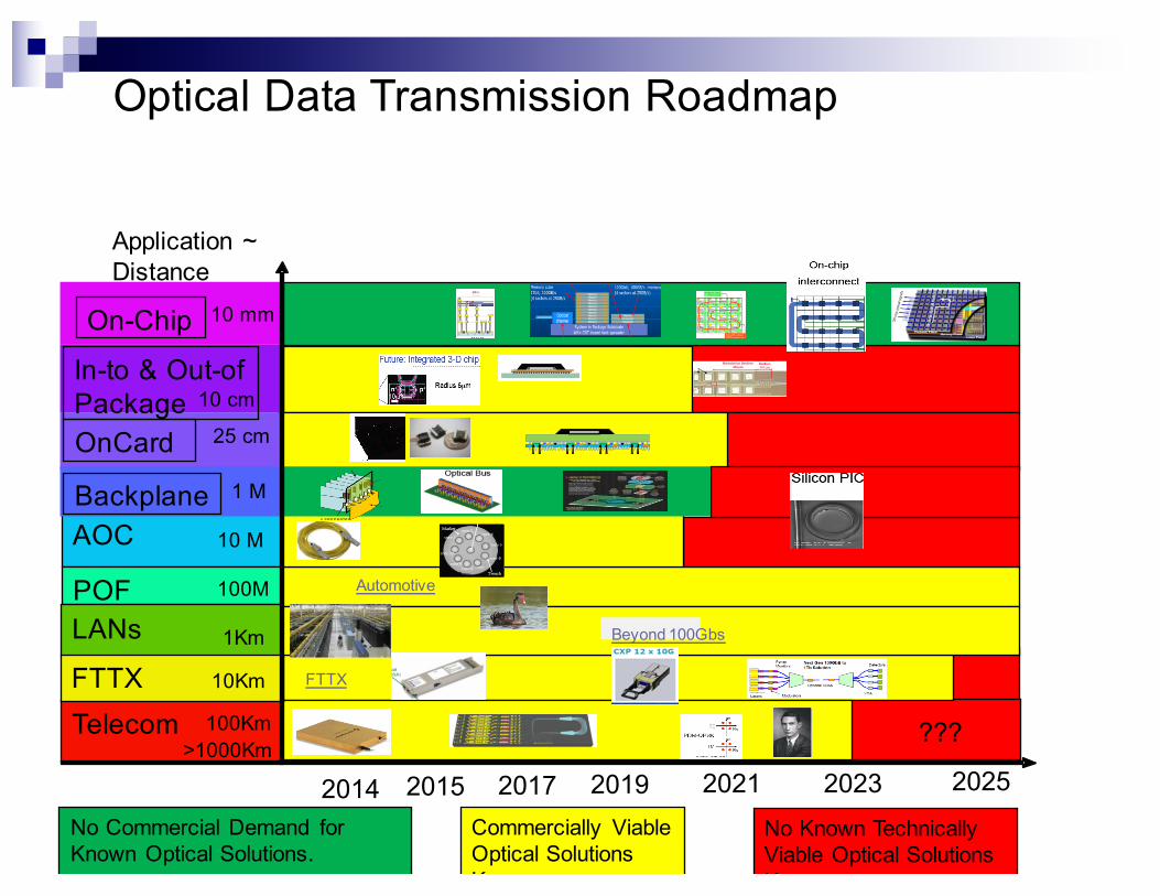
AOC
POF
Telecom
LANs
FTTX
Optical Data Transmission Roadmap
Application ~ Distance
>1000Km
1Km
100M
10 M
25 cm
1 M
100Km
10 mm
10Km
Backplane
In-to & Out-ofPackage
On-Chip
???
Automotive
FTTX
Beyond 100Gbs
OnCard
2014 2017 2019 2021 20252023Commercially Viable Optical Solutions Known
No Commercial Demand for Known Optical Solutions. Electrical Dominates.
No Known Technically Viable Optical Solutions Known
2015
10 cm

40
Results From the Roadmap Activityn The Photonic Systems Manufacturing
Consortium (PSMC) Funded by NIST and Organized under MIT & iNemi’s leadership Was Completed in June of 2016.
n The PSMC #1 Effort was Highly Successful and a Follow On Effort called PSMR Is Continuing as Part of the AIM IP Consortium.
n PSMR is Being Expanded beyond Data Communications to Sensors, Analogue RF and Optical Arrays.

41
The Development Plan for 2017
n Revise and Update the Chapter Utilizing all of the Information Now Available.
n Coordinate with AIM IP and PSMCn Coordinate with Michael Garner, IRDS
Network Connectivity TWG on Optical IO

42
Product Needs
Technology Evolution
Gap Analysis/ Technical
PlanResearch
Projects
Implementation
Competitive Solutions
RoadmapProject
Completion
Industry Solution Needed
Academia
Government
iNEMIUsers & Suppliers
Regional Collaboration
No Work Required or Outsourced
Available to Market
Place
GlobalParticipation
Disruptive Technology
Next Steps: Identify Initiatives to Close Gaps

iNEMI Collaborative Project
Activities

44
• Reduce cost by leveraging resources– Reduce cost by new technologies – Reduce resource demands and $ investments for each company– Stimulate standards and common specification development– Work on issues facing all your suppliers/customers– Disseminate efficient business practices
• Reduce risk of technology introduction – Gain knowledge and accelerate deployment of new technologies – Developing industry infrastructure, source of supply– Ensure reliability and technology readiness when required
• Reduce environmental risks – Ensure sustainable solutions are put in place and in sync with industry
Why Collaborative Projects?

Profile of Successful iNEMI Projects
45
nAddresses knowledge gap of industry¨ Common problem solved by working together¨ Often a pre-cursor to standards development
nBrings together a segment of supply chain to provide industry-wide response
nDirect alignment with member companies’ commercial interests.
Warpage Characterization of Organic PackagesLCA Estimator
Creep Corrosion
Tin Whisker Susceptibility

18 New & Ongoing Projects
46
ProjectName TIG Initiative-StartDate
EstEndDate
BiSnBasedLowTemperature SolderingProcessandReliability BA 8/17/2015 9/30/2017
Characterization ofPb-FreeAlloyAlternatives Project- - AddendumtoScopeofWorkVersion3.2June2,2015
BA 6/30/2017
Characterize andquantifytheinspectioncapability oftheAXIonHoPHiP(Head inPillow)defects
Test 4/23/2015
ConnectorHighSpeedSignalingMetrologyProgram:Phase1 BA 3/31/2016
DC-DCConversionProject- Phase2 9/2/2016
Development ofCleanliness Specification forExpandedBeam Opto 4/29/2016
FinalAssemblyAutomationandOptimization 1/12/2016 9/30/2017
FinePitchCircuit PatternInspection/MetrologyProject Packaging 8/7/2015
HighTemp,Pb-freeDie-AttachMaterial Packaging 9/30/2015
ImpactofLowCTEMoldCompoundonBoardlevelRelability Packaging
PCB/PCBAMaterial Characterization forAutomotiveHarshEnvironments
BA 1/4/2016 5/31/2017
QFNPackageBoardLevel Reliability Project BA 10/15/2014 2/1/2017
Qualification TestDevelopment forCreepCorrosion,Phase3 BA 6/1/2015 2/4/2017
ReuseandRecyclingMetrics - Phase2 ESE 10/28/2015 12/15/2017
SemiconductorPackageMiniaturization TestVehicle forMedicalApplicationsProgram
Medical 4/28/2015 2/28/2017
UltraLowLossLaminate/PCB forHighReliability &Performance OrganicPCB 5/31/2016
ValueRecoveryforEoLElectronics (MetalsPhase2) ESE 12/16/2016
Warpage Characteristics ofOrganicPackagesPhase3 Packaging 6/1/2015 12/11/2016

5 Active Initiatives
47
InitiativeNameiNEMIPM TIG Chair Start
Date
QuantifyImpactofBoardDesignandProcessControltoSMTPerformance HFu BoardAssembly Intel 7/31/2015
SiPModuleMold-abilityStudy M Tsuriya Packaging SCK 12/18/2015
DevelopCleanlinessSpecificationforSingle-ModeandMulti-ModeExpandedBeamConnectors(SMandMM)
DGodlewski Optoelectronics Celestica 6/30/2016
Investigationofmulti-passinterference(MPI)conditionsandconnectorqualityforDataCenterapplications
DGodlewski Optoelectronics Celestica 11/30/2016
Phase2- iNEMIConnectorReliabilityTestRecommendations DGodlewski BoardAssembly 6/30/2016

Completing the 2015 iNEMI Roadmap/Starting the 2017 Cyclen 2015 iNEMI Roadmap Development Cycle is wrapped up!
n 2015 iNEMI Technology Plan Published
n 2015 iNEMI Research Priorities Document Published end of August 2016 & Available Free at www.inemi.org
n 2015 Roadmap Available Free to iNEMI Member Companies
n Available To Industry:n Order the 2015 iNEMI Roadmap flash drive at www.inemi.org
n Individual roadmap chapters are also available as a PDF document download at www.inemi.org
n 2017 iNEMI Roadmap is being developed now for publication to members in late December, 2016 and the industry in late March, 2017¨ Contact Chuck Richardson for more details at [email protected]
48
