atomichjeon.namoweb.net/lecture/4.pdf · 2011-10-18 · atomic structure . atom . nucleus electrons...
TRANSCRIPT

Semiconductor Materials Lab. Hanyang University
Chapter4. Atomic structure

Semiconductor Materials Lab. Hanyang University
적외선 고체 레이저가 1.6mm의 철판을 절단하고 있다. 이 레이저는 네오디뮴(neodymium)이 불순물로 첨가된 YAG(yttrium aluminium garnet)결정을 사용한다. 네오디뮴원자는 작은 반도체 레이저에서 나오는 빛으로 펌핑되며, 이 방법은 매우 효율적인 펌핑 방법이다.
4.1 The Nuclear Atom 4.2 Electron Orbits 4.3 Atomic Spectra 4.4 The Bohr Atom 4.5 Energy levels and Spectra 4.6 Correspondence Principle (대응원리) 4.7 Nuclear Motion 4.8 Atomic Excitation 4.9 The Laser

Semiconductor Materials Lab. Hanyang University
Atomic structure
atom nucleus
Electrons (전자)
protons (양성자)
neutrons(중성자)
electrons circle the nucleus as planets do the sun
classical electromagnetic (em) theory denies the possibility of stable electron orbits.
Niels Bohr applied quantum idea to atomic structure in 1913

Semiconductor Materials Lab. Hanyang University
4.1 The Nuclear Atom
An atom is largely empty space
J.J. Thomson in 1898 suggestion
Atoms are positively changed lumps of matter with electrons embedded in them, like raisins in a fruitcake
Thomson had played an important role in discovering the electron but the real atom turned out to be quite different
Fig4.1 원자의 톰슨(Thomson) 모형. 러더퍼드(Rutherford)산란 실험은 이 모형이 틀렸음을 보였다.

Semiconductor Materials Lab. Hanyang University
Most direct way (done by Hans Geiger and Ernest Marsden. 1911)
use α particle suggested by Rutherford
α particle은 전자 2개를 lost한 charge +2e를 띤 Helium 원자임
fig 4.2 산란 실험 (한 원자두께의 박막)
Semiconductor Materials Lab. Hanyang University
Geiger 와 Marsden의 실험
납 screen 뒤에 α particle 방출 시료를 놓는다
α particle의 narrow beam은 thin gold foil에 입사된다
α particle에 부딪히면 섬광을 내는 zinc sulfide screen를 반대편에 놓는다
α particle was expected to go through the foil with hardly any deflection (Thomson의 model에 의하면)
(Thomson은 전하가 내부에 uniform하게 spread되었다고 했음)
Geiger와 Marsden이 발견한 것
α particle 대부분 굴절 하지 않음 (<1° 이하 굴절)
but 작은 양은 크게 굴절 완전히 반대 방향에서는 발견됨
α particle은 e mass 의 약 8000배이므로 이 같은 현상은 설명 불가

Semiconductor Materials Lab. Hanyang University
이 결과를 설명할 수 있는 방법 (Rutherford의 원자의 핵 Model)
+
Fig 4.3 원자의 러더퍼드(Rutherford)모형.
원자는 양전하를 지니며 원자 질량이 대부분 집중된 작은 핵과 그로부터 다소 떨어진 전자들로 이루어졌다
원자의 대부분은 빈 공간 α particle 그대로 통과
원자의 핵 주위에 접근 α particle 진로에 큰 영향
동일 원소의 원자들은 동일한 핵 전하를 가짐 이 전하량은 주기율표에 따라 증가
핵 전하는 +e의 정수배 원소의 핵이 갖는 단위 양전하의 배수를 원자수(atomic #)라고 함
원자수(atomic #) = 양성자의 수
Semiconductor Materials Lab. Hanyang University
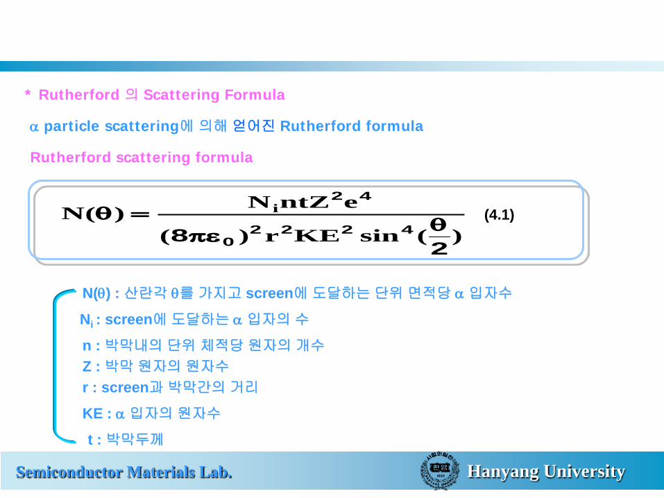
* Rutherford 의 Scattering Formula
α particle scattering에 의해 얻어진 Rutherford formula
Rutherford scattering formula
)(sinKEr)(
entZN)(N i
28 4222
0
42
θπε
=θ
N(θ) : 산란각 θ를 가지고 screen에 도달하는 단위 면적당 α 입자수
Ni : screen에 도달하는 α 입자의 수
n : 박막내의 단위 체적당 원자의 개수 Z : 박막 원자의 원자수 r : screen과 박막간의 거리
KE : α 입자의 원자수
t : 박막두께
(4.1)
Semiconductor Materials Lab. Hanyang University
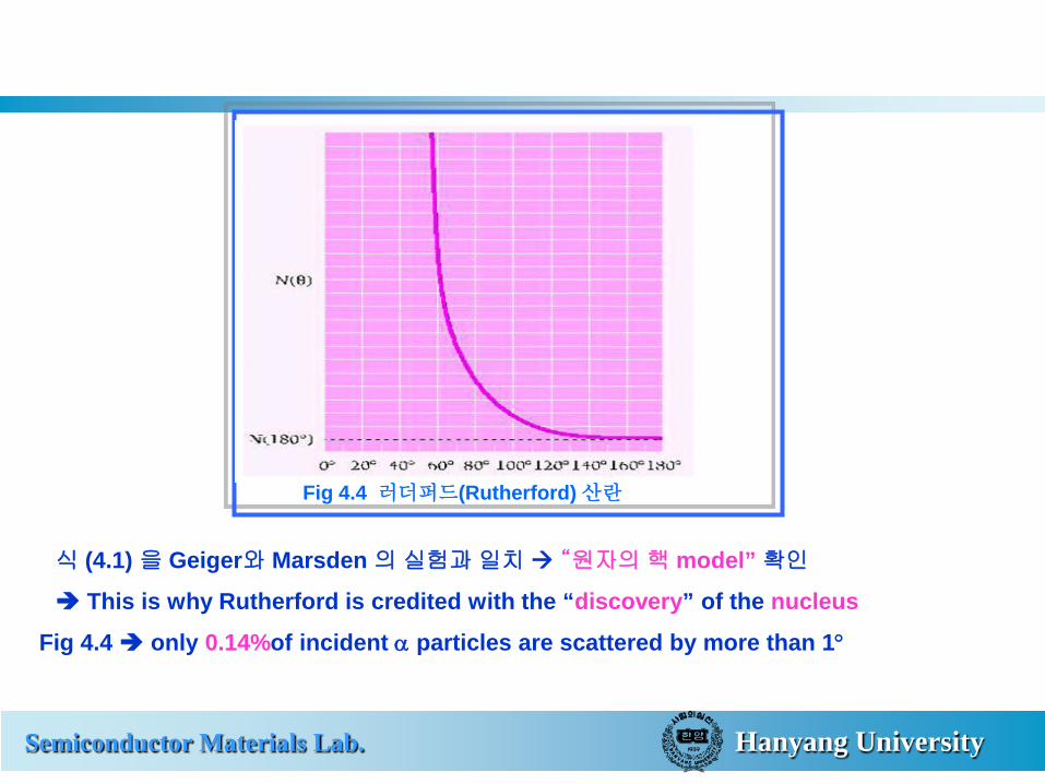
Fig 4.4 러더퍼드(Rutherford) 산란
식 (4.1) 을 Geiger와 Marsden 의 실험과 일치 “원자의 핵 model” 확인
This is why Rutherford is credited with the “discovery” of the nucleus
Fig 4.4 only 0.14%of incident α particles are scattered by more than 1°

Semiconductor Materials Lab. Hanyang University
∗ Nuclear Dimensions
in eq 4.1, Rutherford assumed the size of the target nucleus is small compared with min. distance R
Rutherford scattering gives us a way to find an upper limit to nuclear dimensions
the distance of closest approach R 를 구하려면?
α Particle will have its smallest R when it approach a nucleus head on, which will be followed by a 180° scattering
initial KE of the particle is entirely converted to electric potential E
RZePEKE
2
0
24
1πε
==charge of the α particle :2e
charge of nucleus : Ze
Distance of closest approach
KEZeR0
2
42πε
= (4.2)
Semiconductor Materials Lab. Hanyang University
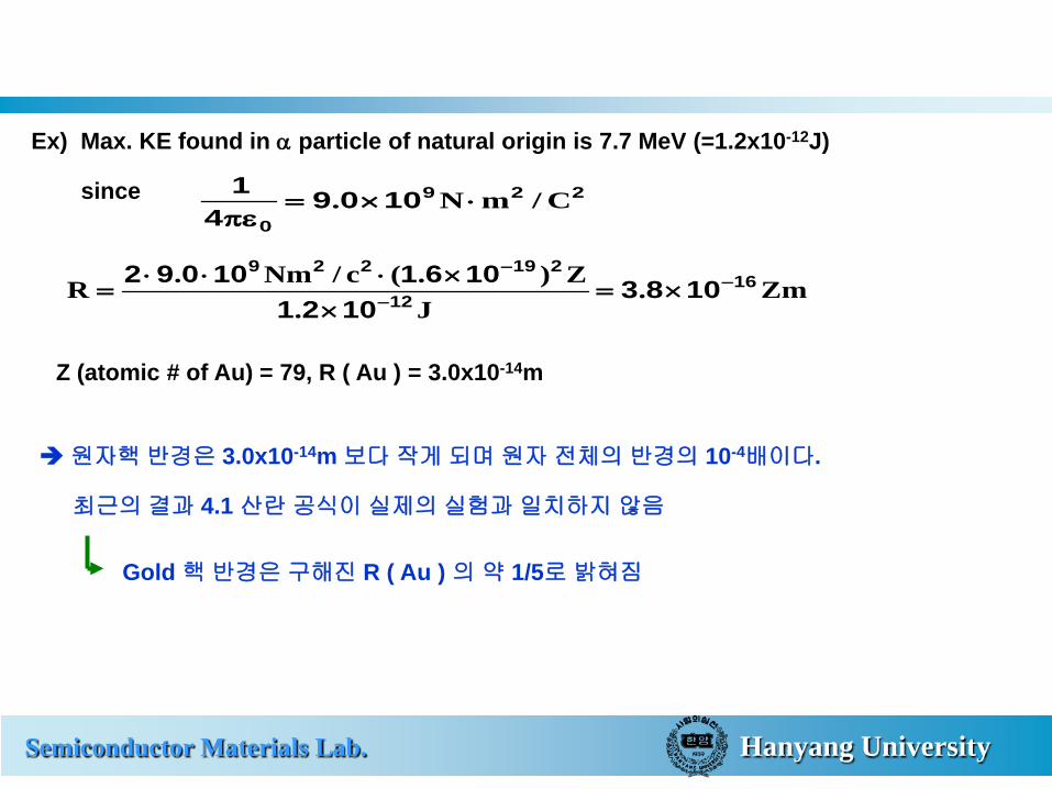
Ex) Max. KE found in α particle of natural origin is 7.7 MeV (=1.2x10⁻¹²J)
since 229
01009
41 C/mN. ⋅×=πε
Zm.J.
Z).(c/Nm.R 1612
2192291083
1021106110092 −
−
−
×=×
×⋅⋅⋅=
Z (atomic # of Au) = 79, R ( Au ) = 3.0x10⁻¹⁴m
원자핵 반경은 3.0x10⁻¹⁴m 보다 작게 되며 원자 전체의 반경의 10-4배이다.
최근의 결과 4.1 산란 공식이 실제의 실험과 일치하지 않음
Gold 핵 반경은 구해진 R ( Au ) 의 약 1/5로 밝혀짐

Semiconductor Materials Lab. Hanyang University
4.2 Electron Orbits
The planetary model of the atom and why it fails
Rutherford 의 원자 Model
positively charged nucleus surrounded at a relatively great distance by enough electrons 전체적으로 전기적 중성
Electrons cannot be stationary If electrons are in motion
태양주위의 행성처럼 안정된 궤도를 가짐
Fig 4.5 수소 원자에서의 힘의 평형
Classical dynamics of H (hydrogen) atom
assume a circular electron orbit (실제로는 타원이지만 simplify하기 위해)
the centripetal force r
mvFc
2
=
electric force 2
2
041
reFe πε
=

Semiconductor Materials Lab. Hanyang University
condition for dynamically stable orbit
electron velocity ν
mre
04πε=ν (4.4)
total E of electron =KE+PE
2
21 mvKE = r
ePE0
2
4πε−=
remvPEKEE
0
22
42 πε−=+=
ec FF = (4.3) , 2
0
22
4 re
rmv
πε=
Substituting for ν from eq 4.4 gives
re
re
reE
0
2
0
2
0
2
848 πε−=
πε−
πε= (4.5)

Semiconductor Materials Lab. Hanyang University
total E of e is -νe atomic electrons and bound to the nucleus
If total E of e is +νe e will not follow a closed orbit around nucleus
* Failure of Classical Physics
Pillar of classical physics
Newton’s laws of motion
Coulomb’s law of electric force 이 두 이론은 전자가 안정하다는 실험결과와 일치
Maxwell’s electromagnetic theory 불일치
가속되는 전자(electric charge)는 전자파의 형태로 에너지 방출
나선을 그리며 핵 속으로 들어가야 된다
실제로는 원자가 붕괴되지 않는다
실험결과 불일치
Semiconductor Materials Lab. Hanyang University
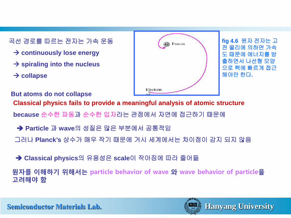
곡선 경로를 따르는 전자는 가속 운동
continuously lose energy
spiraling into the nucleus
collapse
But atoms do not collapse Classical physics fails to provide a meaningful analysis of atomic structure
fig 4.6 원자 전자는 고전 물리에 의하면 가속도 때문에 에너지를 방출하면서 나선형 모양으로 핵에 빠르게 접근해야만 한다.
because 순수한 파동과 순수한 입자라는 관점에서 자연에 접근하기 때문에
Particle 과 wave의 성질은 많은 부분에서 공통적임
그러나 Planck’s 상수가 매우 작기 때문에 거시 세계에서는 차이점이 감지 되지 않음
Classical physics의 유용성은 scale이 작아짐에 따라 줄어듦
원자를 이해하기 위해서는 particle behavior of wave 와 wave behavior of particle을 고려해야 함

Semiconductor Materials Lab. Hanyang University
* Is Rutherford’s Analysis Valid?
Rutherford는 그의 scattering formula를 atomic stability 관점에서 맞지 않는 물리법칙을 사용
즉 고전 물리학을 이용하여 formula를 완성
실제 Rutherford의 최소거리 R을 3x10-14m로 De Broglie파의 약 6배정도로서 이러한 상호작용의 α 입자는 고전적 입자로 간주 할 수 있다
원자는 작은 핵을 중심으로 전자가 멀리 떨어져서 그 주위를 둘러 쌓고 있다는 것은 Rutherford model이 α particle로 증명이 가능하다
그러나 원자내의 전자는 nonclassical approach가 요구 된다
2.0x10⁷m/s를 갖는 α입자의 De Broglie파장
m.s/m.Kg.
SJ.mh 15
727
341005
1002106610636 −
−
−
×=×⋅×⋅×
=ν
=λ

Semiconductor Materials Lab. Hanyang University
4.3 Atomic Spectra
Each element has a characteristic line spectrum
•Atomic stability 뿐만 아니라
spectral lines이 존재하는 것은 classical physics로 설명이 불가능
* Condensed matter (solids and liquids) 는 모든 온도에서 모든파장의 전자기파를 발산
Planck는 radiation의 feature을 설명하였으나 어떻게 되는지에 관한 설명 없다
즉 특정한 원소의 특성적인(characteristic ) 거동이라기 보다는 상호 작용하는
수많은 원자들의 집단적인(collective) 거동으로 봄
그러나 한 극단의 경우 원자나 분자가 충돌을 하는 경우 원자나 분자의 특정적인 (characteristic) 파를 방출한다.

Semiconductor Materials Lab. Hanyang University
실제의 분광기에서는 diffraction grating (회절격자)를 사용한다
fig4.7 이상적인 분광기
* Atomic gas나 vapor가 대기압 보다는 작은 압력에 있게 되면 전류를 흘러주어서 excite 시키게 된다 emitted radiation 어떤 특정(characteristic) 파장만이 포함된 spectrum을 갖게 된다

Semiconductor Materials Lab. Hanyang University
Fig. 4.8 수소, 헬륨, 수은 방출 스펙트럼의 주된 선들.
Emission line spectra of several elements
Every element display a unique line spectrum
Spectroscopy is a useful tool for analyzing the composition of an unknown substance

Semiconductor Materials Lab. Hanyang University
When white light is passed through a gas
gas absorb light of certain wavelengths
Absorption line spectrum (consists of a bright background crossed by dark lines (missing λ))
전류에 의해 여기된 관속에 들어 있는 가스 원자는 가스 특성 파장의 빛을 낸다.

Semiconductor Materials Lab. Hanyang University
Fig4.9 한 원소의 흡수 스펙트럼에서의 어두운 선은 그 원소의 방출 스펙트럼에서의 밝은 선에 대응된다.
spectrum of sunlight has dark line
sun is surrounded by an envelope of cooler gas that absorbs certain λ only
the number, strength, and exact λ of lines in the spectrum of an element depend upon temp., pressure, presence of electric magnetic fields and the motion of the source

Semiconductor Materials Lab. Hanyang University
* Spectral Series
The wavelengths in the spectrum of an element were found to fall into sets called “spectral series”
The 1st such series was found by J.J Balmer in 1885
( 수소원자 spectrum의 가시광선 영역을 연구하다 발견)
Fig4.10 수소의 발머(Balmer) 계열.
가장 긴 파장 656.3nm(red) 다음 파장 486.3nm(blue)
계열 한계(series limit) 364.6nm
이 이상에서는 더 이상 분리된 선으로 나타나지 않으며 희미한 연속 spectrum을 보여준다

Semiconductor Materials Lab. Hanyang University
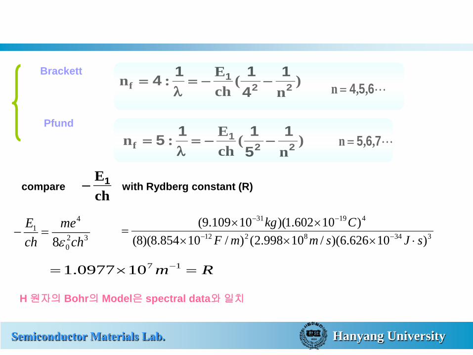
Balmer’s formula
)n
(R 221
211−=
λn= 3,4,5,······
R : Rydberg constant
R=1.097x10⁷m-1=0.01097nm-1
series limit n=∞ λ=4/R agree with experiment
Balmer series contains λ in the visible portion of the hydrogen spectrum
Spectral lines of H in the UV infrared regions fall into several other series
in ultraviolet the Lyman series
Lyman
)n
(R 221
111−=
λ n= 2,3,4,·····

Semiconductor Materials Lab. Hanyang University
in the infrared
Paschen )
n(R 22
1311−=
λn= 4,5,6,·····
Brackett )
n(R 22
1411−=
λ n= 5,6,7,·····
Pfund )
n(R 22
1511−=
λn= 6,7,8,·····
Fig4.11 수소의 스펙트럼 계열, 각 계열의 파장은 간단한 식과 연관된다.

Semiconductor Materials Lab. Hanyang University
4.4 The Bohr Atom
Electron waves in the atom
the first theory of atom by Niels Bohr in 1913
De Broglie가 발견한 것과 같이 matter wave에 관한 개념이 이 이론에서 도출되었다
- De Broglie 보다 10년 정도 앞선 것으로서 다른 이론 사용
수소 핵 주위의 전자의 파동성으로 부터 시작됨
이 전자의 De Broglie 파(λ)
mvh
=λ
v is element velocity
mrev
04πε=
Orbital electron wavelength
mr
eh 04πε
=λ (4.11)

Semiconductor Materials Lab. Hanyang University
r=5.3∗10-11m for radius of the e orbit then electron λ
mKg
mmFC
SJ 1131
1112
11
34
1033101.9
)103.5)(/1085.8)(4(106.1
1063.6 −−
−−
−
−
×=×
×××
⋅×=
πλ
This wavelength is exactly the same as the circumference of the electron orbit
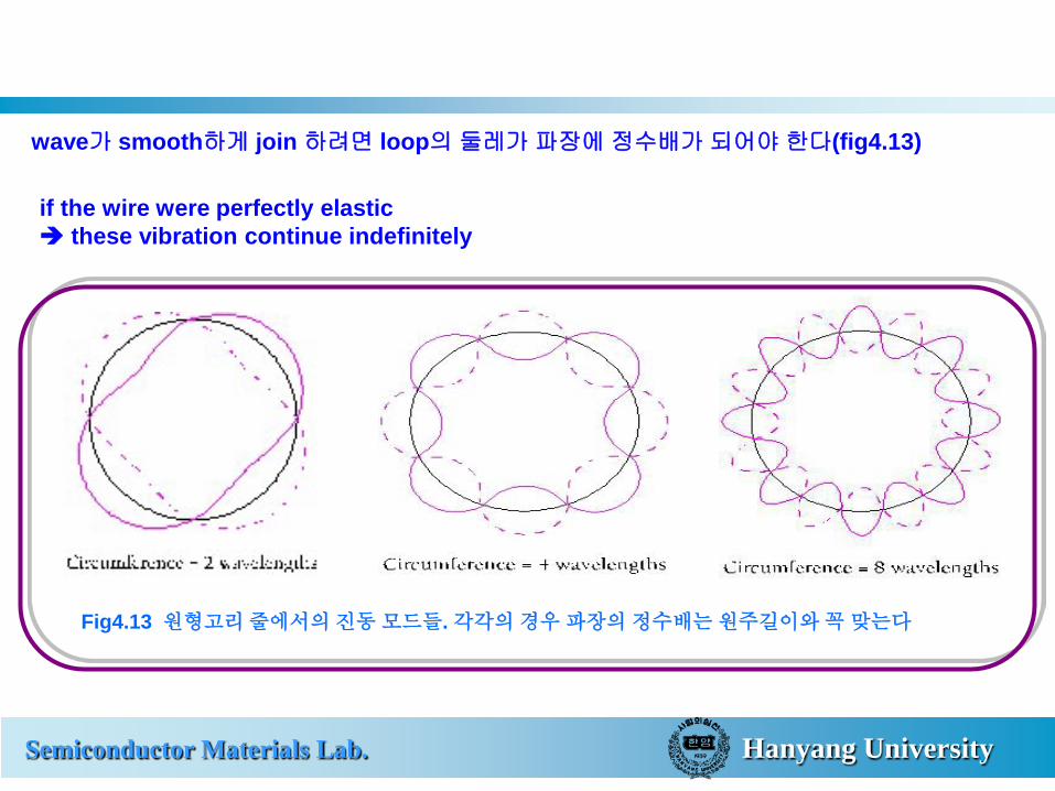
Fig4.12 수소 원자의 전자 궤도는 양 끝점이 연결된 전자의 완전한 하나의 de Broglie 파동에 해당한다
mr 1110332 −×=π
The orbit of electron in H atom corresponds to one complete electron wave joined on itself
수소원자에서는 전자궤도의 둘레가 전자의 한 파장이라는 사실은 원자의 이론을 수립하는데 매우 중요
Semiconductor Materials Lab. Hanyang University
Fig4.13 원형고리 줄에서의 진동 모드들. 각각의 경우 파장의 정수배는 원주길이와 꼭 맞는다
wave가 smooth하게 join 하려면 loop의 둘레가 파장에 정수배가 되어야 한다(fig4.13)
if the wire were perfectly elastic these vibration continue indefinitely

Semiconductor Materials Lab. Hanyang University
fig4.14 원주 길이가 파장의 정수배가 아닌 경우 상쇄 간섭이 일어나므로, 오래 지속될 수 없게 된다.
고리에 따라 정수배가 아닌 파장의 vibration
Destructive interference
Vibration will die out rapidly
윗 결과로부터
An electron can circle a nucleus only if its orbit contains an integral of de Broglie wavelengths
전자의 wavelength는 nucleus를 끄는 힘(Fe)와 balance를 이루기 위한 orbital velocity에 의존되기 때문에 윗가설은 전자의 입자성과 파동성을 종합한 것으로 볼 수 있다( 즉 matter wave)

Semiconductor Materials Lab. Hanyang University
Condition for orbit stability
nrn π=λ 2 ⋅⋅⋅= 321 ,,n (4.12) rn: n개 파장을 포함하는 궤도 반경
n: quantum number
substituting for λ by eq4.11
nn r
mr
enh ππε 24 0 = ⋅⋅⋅= 3,2,1n
Orbital radii in Bohr atom
20
22
mehnrn πε
= ⋅⋅⋅= 321 ,,n
최내각 궤도의 반경을 관습적으로 수소원자의 Bohr radius라고 한다 (a0)
Bohr radius m.ra 1110 102925 −×==
other radii are given by a0 by the formula 0
2anrn =
(4.13)

Semiconductor Materials Lab. Hanyang University
4.5 Energy level and Spectra
A photon is emitted when an electron jumps from one energy level to a lower level
electron energy En is given by r n n
n reE
0
2
8πε=
substituting for r n from eq 4.13
Energy levels
21
2220
4 18 n
E)n
(h
meEn =ε
= ⋅⋅⋅= 321 ,,n (4.15)
eV.J.E 61310182 181 −=×−= −
Semiconductor Materials Lab. Hanyang University
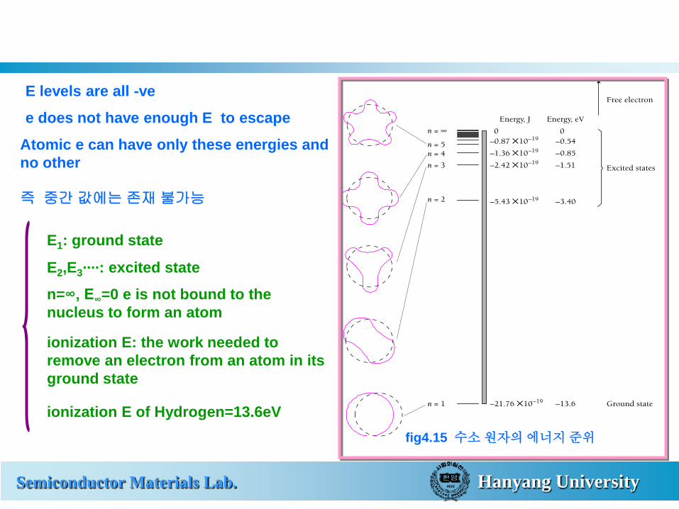
E levels are all -ve
e does not have enough E to escape
Atomic e can have only these energies and no other
즉 중간 값에는 존재 불가능
E1: ground state
E2,E3····: excited state
n=∞, E∞=0 e is not bound to the nucleus to form an atom
ionization E: the work needed to remove an electron from an atom in its ground state
ionization E of Hydrogen=13.6eV fig4.15 수소 원자의 에너지 준위

Semiconductor Materials Lab. Hanyang University
Origin of Line Spectra
Atoms exhibit line spectra in both emission and absorption
electron in a excited state drops to a lower state
lost E is emitted as a single photon of light
electron은 어떤 특정한 에너지 준위에만 존재
photon은 gradual 한 방법이 아니라 한번에 하나의 photon으로 방출
quantum # of initial state : n i quantum # of final state : n f
initial E - final E =photon E υ=− hEE fi (4.16)
from eq 4.15
)11()11( 22221fi
nfi
fi nnE
nnEEE −−=−=−
Semiconductor Materials Lab. Hanyang University
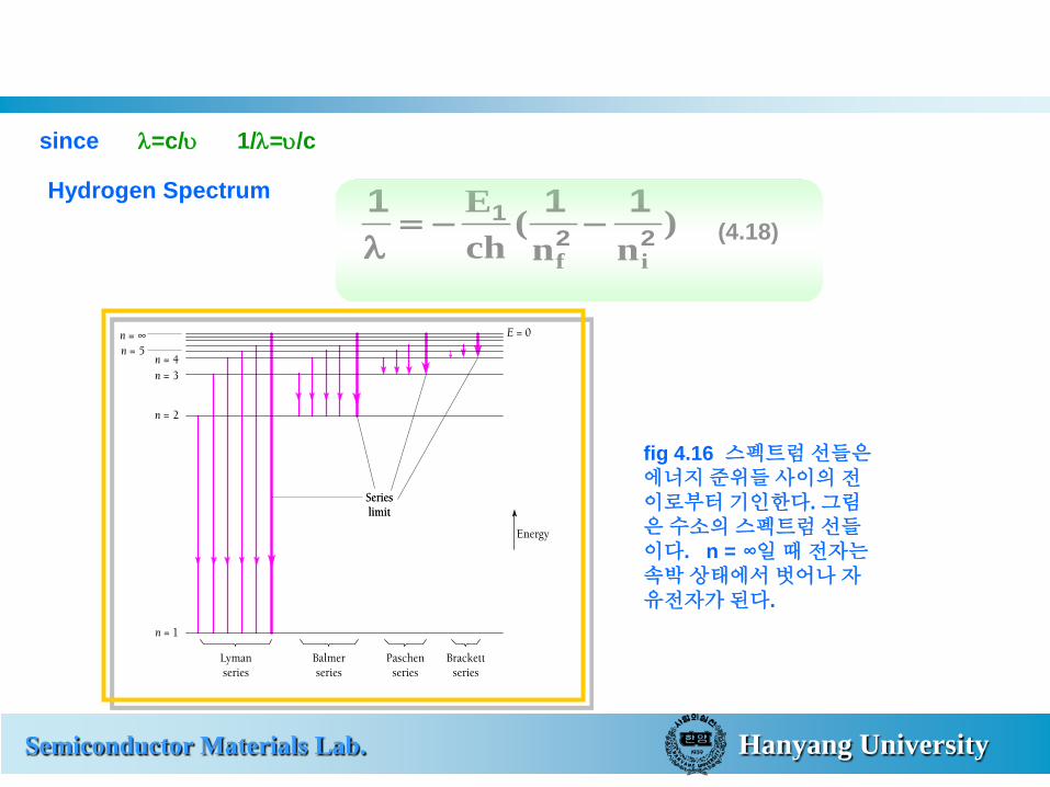
since λ=c/υ 1/λ=υ/c
Hydrogen Spectrum )
nn(
chE
if22
1 111−−=
λ (4.18)
fig 4.16 스펙트럼 선들은 에너지 준위들 사이의 전이로부터 기인한다. 그림은 수소의 스펙트럼 선들이다. n = ∞일 때 전자는 속박 상태에서 벗어나 자유전자가 된다.

Semiconductor Materials Lab. Hanyang University
eq4.18 radiation emitted by excited H atom should contain certain wavelengths only
These λ fall into definite sequences
Lyman )1
11(1:1 22
1
nchEn f −−==
λ⋅⋅⋅= 4,3,2n
Balmer
)121(1:2 22
1
nchEn f −−==
λ⋅⋅⋅= 5,4,3n
Paschen
)131(1:3 22
1
nchEn f −−==
λ⋅⋅⋅= 5,4,3n
Semiconductor Materials Lab. Hanyang University
Pfund )
n(
chE:nf 22
1 15115 −−=
λ= ⋅⋅⋅= 765 ,,n
Brackett )
n(
chE:nf 22
1 14114 −−=
λ= ⋅⋅⋅= 654 ,,n
compare chE1− with Rydberg constant (R)
320
41
8 chme
chE
ε=− 3348212
41931
)10626.6)(/10998.2()/10854.8)(8()10602.1)(10109.9(
sJsmmFCkg
⋅×××××
= −−
−−
Rm =×= −17100977.1
H 원자의 Bohr의 Model은 spectral data와 일치

Semiconductor Materials Lab. Hanyang University
4.6 Correspondence principle (대응원리)
The greater the quantum number, the closer quantum physics approaches classical physics
quantum physics
different from classical physics in the microworld give the same result as classical physics in the macroworld
(움직이는 물체의 파동 이론에서 증명됨)
전자기학 이론에 의하면 an electron moving in a circular orbit radiates em waves whose frequency are equal to its frequency of revolution(공진 진동수) and to harmonics of that frequency(진동수의 정수배가 되는 파(고조파))
in H-atom, the electron’s speed is
mre
04πευ = r: radius of its orbit
frequency of revolution ƒ of the electron is
30422 mr
ercecircumfernorbit
speedelectronfπεππ
υ===

Semiconductor Materials Lab. Hanyang University
Radius r n of a stable orbit is given in terms of its quantum number (n) by eq4.13
20
22
mehnrn πε
=
frequency of revolution
(고전역학) )n
(hE)
N(
hmef 3
1332
0
4 228
−=ε
= (4.19)
Under what circumstances should Bohr atom behave classically?
if e orbit is so large Quantum effect is negligible
0.01mm of orbit meet this specification
its quantum number is n=435
(possible only in theory)
H atoms in such state never occur in nature

Semiconductor Materials Lab. Hanyang University
What does the Bohr theory predict such an atom will radiate? H atom dropping from nith energy level to nfth energy level
emits a photon whose frequency is
)nn
(hE
if22
1 11−
−=υ
let) n i=n n f=n-p (p=1,2,3···) with this substitution
])pn(n
pnp[hE]
n)pn([
hE
22
21
221 211
−−−
=−−
−=υ
n i & n f are both very large n>>p nppnp 22 2 ≈−22 n)pn( ≈−
so that
Frequency of photon
(양자역학) )
np(
hE
31 2−
=υ (4.20)
Semiconductor Materials Lab. Hanyang University
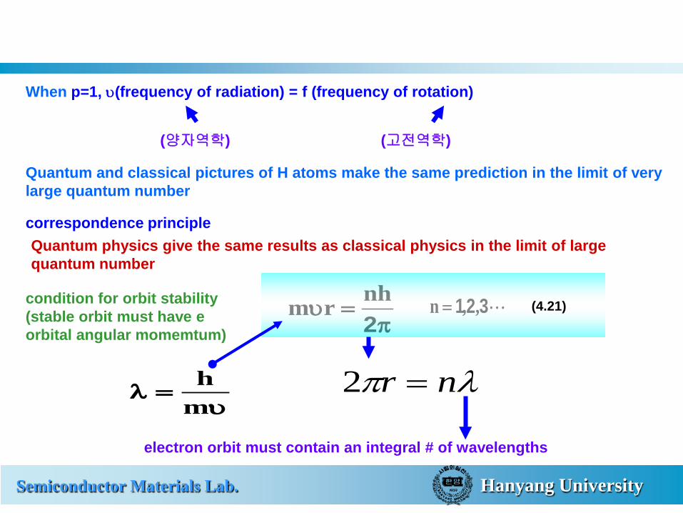
When p=1, υ(frequency of radiation) = f (frequency of rotation)
(양자역학) (고전역학)
Quantum and classical pictures of H atoms make the same prediction in the limit of very large quantum number
correspondence principle Quantum physics give the same results as classical physics in the limit of large quantum number
condition for orbit stability (stable orbit must have e orbital angular momemtum) π
=υ2nhrm ⋅⋅⋅= 321 ,,n (4.21)
υ=λ
mh λπ nr =2
electron orbit must contain an integral # of wavelengths

Semiconductor Materials Lab. Hanyang University
정 리 1. 보어의 가설 1— 원자 내에 전자는 어떤 특정한 조건을 만족하는 원 궤도에서만 안정된 운동을 하며 이 궤도를 운동하는 전자는 전자기파를 발생하지 않고 안정된 상태를 유지한다
2. 보어의 가설 2— 전자가 한 안정한 궤도에서 다른 안정한 궤도로 이동(전이)하는 경우, 두 정상 상태의 에너지 차이만큼 광파를 방출하거나 흡수한다. 궤도 반경은 n2에 비례하여 커지는 것이다.

Semiconductor Materials Lab. Hanyang University
Bohr 의 문제점 1. 전체가 아닌 몇 원자만 설명 가능 (수소 등) 2. Selection rule이 설명 안됨 -보어의 원자 모형은 수소 원자의 에너지 준위에 따른 광자의 방출과 흡수를 통하여 수소의 선스펙트럼을 설명할 수 있고, 수소 원자와 같이 전자가 하나 뿐인 다른 원자의 경우에는 전자의 궤도를 구체적으로 설명할 수 있다. 그러나 전자수가 많아지면 원자에서 나오는 스펙트럼을 설명할 수 없어지며, 전자 하나 하나의 궤도를 보어의 방법으로는 계산할 수도 없다. - 가속 운동하는 전하에 의하여 전자기파가 발생한다는 전자기이론이 어떻게 원자 내부에서 가속 운동을 하는 전자가 정상 상태에서 전자기파를 방출하지 않는가에 대해서는 그 이유를 설명하지 못한다. - 전자를 드브로이의 물질파로 생각해 보면, 전자의 위치는 물질파의 파면에서 어느 순간에 어느 지점에 있는지를 알 수 없게 되기 때문에 전자는 보어가 주장하듯 특정한 궤도에서 원운동을 하고 있다고 볼 수 없게 된다.

Semiconductor Materials Lab. Hanyang University
4.7 Nuclear Motion
The nuclear mass affects the wavelengths of spectral lines
Thus far 수소의 핵(양성자)는 정지해 있고 궤도전자(orbital electron) 는 그 주위를 돈다고 가정
실제는 nuclear와 electron 둘 다 common center of mass 주위를 돈다
그러나 이 질량중심은 핵에 더욱 가깝다 (∴m핵 >> m전자)
If m is the electron mass and M is the nuclear mass
reduced mass m'?
Reduced mass
MmmM'm+
= (4.22)
Reduced mass of electron (its value is less than m)

Semiconductor Materials Lab. Hanyang University
fig 4.17 수소 원자의 전자와 핵 둘 모두가 그들의 공통 질량중심 주위를 돈다 (실제 척도가 아님)
M
The motion of nucleus in the H atom replace the e with particle of mass m'
Energy levels corrected for nuclear motion
))('()1(8
'21
2220
4'
nE
mm
nhemEn =−=
ε (4.23)
핵의 운동에 따른 수소의 모든 에너지 준위는
99945.0' =+
=Mm
mMm 의 비율만큼 변함
Semiconductor Materials Lab. Hanyang University
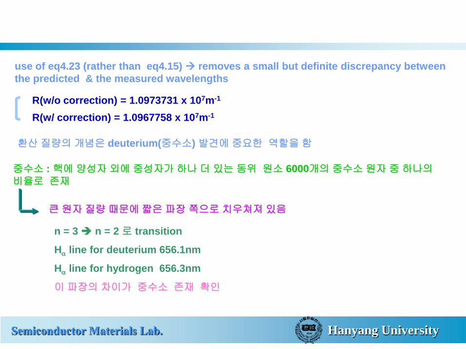
use of eq4.23 (rather than eq4.15) removes a small but definite discrepancy between the predicted & the measured wavelengths
R(w/o correction) = 1.0973731 x 10⁷m-1
R(w/ correction) = 1.0967758 x 10⁷m-1
환산 질량의 개념은 deuterium(중수소) 발견에 중요한 역할을 함
중수소 : 핵에 양성자 외에 중성자가 하나 더 있는 동위 원소 6000개의 중수소 원자 중 하나의 비율로 존재
큰 원자 질량 때문에 짧은 파장 쪽으로 치우쳐져 있음
n = 3 n = 2 로 transition
Hα line for deuterium 656.1nm
Hα line for hydrogen 656.3nm
이 파장의 차이가 중수소 존재 확인

Semiconductor Materials Lab. Hanyang University
오로라(Aurora)는 성층권에서 태양으로부터 오는 빠른 양성자와 전자에 의해 원자가 여기되어 생긴다. 오로라에서의 푸른색 색조는 산소에 의한 것이며, 붉은색은 산소와 질소 양쪽으로부터 온다. 그림에서의 오로라는 알래스카(Alaska)에서 발생한 것이다.

Semiconductor Materials Lab. Hanyang University
4.8 Atomic Excitation
How atoms absorb and emit energy
two main ways (원자를 ground state에서 excite 시켜 복사선을 방출하는 2가지 법)
① collision with another particle
part of KE absorb by an atom
excited atom return to its ground state
emit one or more photons
fig 4.18 충돌에 의한 여기. 한 원자가 유효한 에너지를 흡수하여 들뜬 상태로 전이된다. 그 원자가 바닥 상태(정상 상태)로 돌아오면서 광자 한 개를 방출한다.
희박한 기체에서 luminous discharge(형광반전)을 일으키기 위해서 전자나 원자이온을 충분한 KE를 갖도록 전기장을 가속 시켜서 원자를 excite 시킨다
이와 같은 방전을 전자가 이온보다 효과적임
ex) Neon signs & mercury vapor lamp
↓ ↓
red light bluish light
Semiconductor Materials Lab. Hanyang University
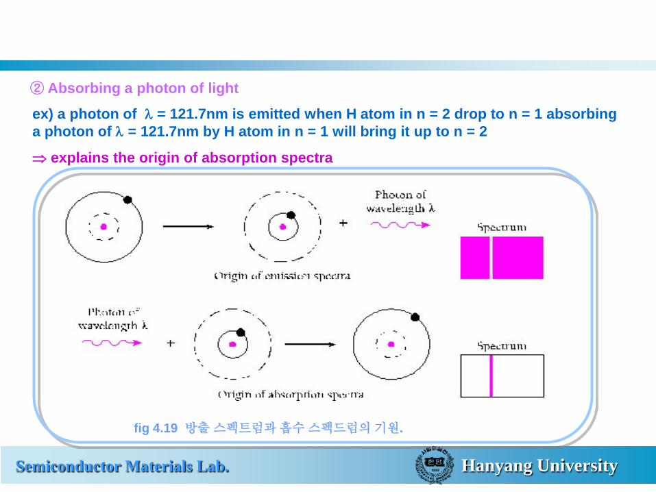
② Absorbing a photon of light
ex) a photon of λ = 121.7nm is emitted when H atom in n = 2 drop to n = 1 absorbing a photon of λ = 121.7nm by H atom in n = 1 will bring it up to n = 2
⇒ explains the origin of absorption spectra
fig 4.19 방출 스펙트럼과 흡수 스펙드럼의 기원.

Semiconductor Materials Lab. Hanyang University
white light ( contain all λ ) is passed through H gas
photon of those λ that correspond to transitions between energy level are absorbed
resulting excited H atom reradiate their excitation energy
But these photon come off in random direction
dark lines in an absorption spectrum are never be completely black
fig4.20 흡수 스펙트럼에서의 어두운 선은 완전히 깜깜한 것만은 결코 아니다.

Semiconductor Materials Lab. Hanyang University
∗ Franck – Hertz Experiment
Atomic spectra are not the only way to investigate energy level inside atoms
Experiments based on excitation by collision was performed
fig 4.21 프랑크-헤르츠(Franck-Hertz)의 실험 장치.
These experiments demonstrated the atomic energy level

Semiconductor Materials Lab. Hanyang University
F-H experiment
• bombarded the vapors of various elements with electrons of known energy
• small potential difference V0 between the grid & collecting plate
prevents electrons having energy less than a min. from contributing to the current I
• As the accelerating potential V is increased , more electrons arrive at the plate and I rises
fig4.22 수은 기체에서의 임계 퍼텐셜을 보여주는 Franck-Hertz 실험의 결과.
Semiconductor Materials Lab. Hanyang University
전자와 원자의 충돌에서 KE가 보존 된다면 전자는 단지 다른 방향으로 튀어 나갈 뿐이다.
∴atom은 electron 보다 매우 무거워서 충돌 시 e 은 KE를 거의 잃지 않는다
그러나 어떤 critical energy 에서는 plate current가 갑자기 drop한다
suggestion e 이 원자와 충돌 시 원자를 excite state를 만들기 위해 전자가 KE의 전부 혹은 부분을 원자에 주기 때문으로 해석
이와 같은 충돌은 비 탄성(inelastic) collision 이라고 함
( elastic collision 은 KE가 conserved 됨)
The critical electron energy equals the energy needs to raise the atom to its lowest excited state
accelerating potential voltage가 더 올라가면 plate current는 다시 커지고 다시 sharp 한 drop이 생기는데 이것은 다른 원자를 동일한 energy level 로 여기 시키기 때문이다
As fig4.22
특정 원자에 대해 일련의 임계전위
Semiconductor Materials Lab. Hanyang University
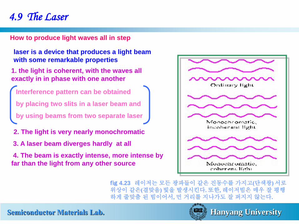
4.9 The Laser
How to produce light waves all in step
laser is a device that produces a light beam with some remarkable properties
fig 4.23 레이저는 모든 광파들이 같은 진동수를 가지고(단색광) 서로 위상이 같은(결맞음) 빛을 발생시킨다. 또한, 레이저빔은 매우 잘 평행하게 줄맞춤 된 빔이어서, 먼 거리를 지나가도 잘 퍼지지 않는다.
1. the light is coherent, with the waves all exactly in in phase with one another
Interference pattern can be obtained
by placing two slits in a laser beam and
by using beams from two separate laser
2. The light is very nearly monochromatic
3. A laser beam diverges hardly at all
4. The beam is exactly intense, more intense by far than the light from any other source

Semiconductor Materials Lab. Hanyang University
Laser = light amplification by stimulated emission of radiation
usual lifetime of excited energy level : 10-8s
metastable excited state lifetime: 10-3s
fig 4.24 어떤 원자는 빛을 방출하기 전까지 보통의 에너지 준위보다 더 오래 머무는 준안정 에너지 준위를 가질 수 있다.

Semiconductor Materials Lab. Hanyang University
three kinds of transition involving electromagnetic radiation between E0 & E1
Induced absorption
fig 4.25 두 원자 에너지 준위 사이의 전이는 유도 흡수, 자발 방출, 유도 방출에 의해 일어난다.
1) Induced absorption
the atom initially lower state E0 raised to E1 by absorbing a photon of energy E1 - E0 =hυ
2) Spontaneous emission
the atom initially upper state E1 drop E0 by emitting a photon of energy
E =h υ
Semiconductor Materials Lab. Hanyang University
3) Induced emission ( Einstein이 1917년 가능성 지적)
the incident photon ( hυ ) cause a transition from E1 to E0
the radiated light waves are exactly in phase with incident one
the result is an enhanced beam of coherent light
induced emission has the same possibility as induced absorption
Induced emission No nobel concept ( 고상한 개념이 아님)
An analogy is a harmonic oscillator
Pendulum을 생각하면 가해준 힘이 in phase 면 진폭 2배
가해준 힘이 180°차이가 나면 진폭 줄어듦
Semiconductor Materials Lab. Hanyang University
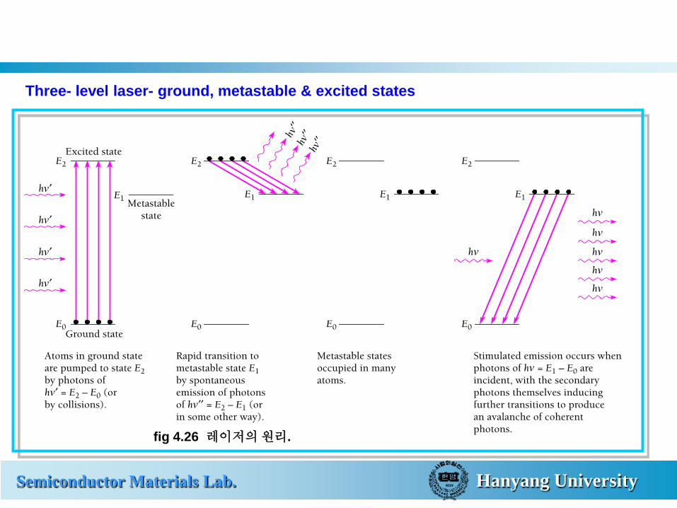
Three- level laser- ground, metastable & excited states
fig 4.26 레이저의 원리.

Semiconductor Materials Lab. Hanyang University
More atoms in metastable state than in ground state
Shine light of frequency υ (hυ) on the assembly
More induced emission from atoms in the metastable state
Result will be an amplification of the original light
Population inversion
Majority are in energy levels above the ground state
( normally the ground state is occupied the greatest extent)
Ways to produce a “ population inversion ”
One of them is “ optical pumping ”

Semiconductor Materials Lab. Hanyang University
fig 4.27 루비 레이저. 유도 방출이 유도 흡수보다 많이 일어나기 위해서는, 루비 막대에 있는 Cr^3+` 이온들의 반 이상이 준 안정 상태에 있어야만 한다. 레이저는 램프가 터질 때마다 붉은색 빛의 펄스를 발생시킨다.
Optical pumping
External light source is used
Photons raised to the excited state from the ground state
Decay spontaneously to the desired metastable state

Semiconductor Materials Lab. Hanyang University
Four –level laser
Intermediate state존재
( unstable)
Laser transition은 metastable state에서 unstable한 intermediate state에서 끝난다
( ground state로 전이는 three- level에서 발생)
intermediate state에서 ground state로 매우 빠르게 transition이 발생 ( very few atoms are in intermediate state)
laser 증폭을 위해 적당히 pumping 해주면 intermediate state보다 metastable state에 충분히 많은 원자 즉 밀도증가 fig 4.28 4-준위 레이저.

Semiconductor Materials Lab. Hanyang University
피복공장에서 옷감을 자르기 위해 로봇 팔에 레이저가 장착되어 있다.

Semiconductor Materials Lab. Hanyang University
∗ Practical lasers
Ruby laser (fig4.27) three level laser
Al2O3 crystal some of Al3+ are replaced Cr3+
( responsible for the Red color)
Cr3+ ion has metastable level whose lifetime is ~0.003secs
In ruby laser Xe flash lamp excites Cr3+ ion to a excited state
fall to metastable level by losing energy
photons from spontaneous decay of Cr3+ are reflected back & forth
between the mirrored ends
stimulating other excited Cr3+ ions to radiate
after a few µsec, a large pulse of monochromatic, coherent, red light
form the partly transparent end of the rod

Semiconductor Materials Lab. Hanyang University
Helium- neon gas laser
Achieve a population inversion in a different way
He과 Ne이 10:1로 혼합된 기체를 1torr의 압력으로 양끝이 평행한 거울로 된 유리관에 봉입
한다 ( 하나는 partly transparent, 거울 사이의 laser의 반파장의 정수배)
electric discharge is produced
collision with electrons excite He & Ne to metastable state, 20.61 & 20.66eV
some of excited He transfer E to ground state Ne atoms in collision
0.05eV of additional E provided by the KE atoms
the purpose of He atoms is to help achieve a population inversion in Ne atoms
laser transition of Ne from metastable state 20.66eV to excited state 18.7eV with
emission of 632.8nm photon

Semiconductor Materials Lab. Hanyang University
another photon is spontaneously emitted in a transition to a lower metastable state
incoherent light
remaining excitation E is lost in collision with tube wall
He-Ne laser operates
used to read a bar code( 붉은색 광선)
fig4.29 헬륨-네온 레이저. 이와 같은 4-준위 레이저에서는 연속적인 레이저 발진이 가능하다. 헬륨-네온 레이저는 바 코드를 읽는데 흔하게 쓰이고 있다.

Semiconductor Materials Lab. Hanyang University
Chemical laser 원자 대신 분자 이용
Based on the production by chemical reactions of molecules in metastable excited states
very efficient & very powerful
H (hydrogen) & F (fluorine) combine to from HF
generated infrared beam of over 2MW
dye laser (염색 laser) use dye molecule
can “ lase ” virtually continuous range of λ
can be tuned to any desired λ in its range

Semiconductor Materials Lab. Hanyang University
Carbon dioxide gas laser
~100W급의 경우 생체조직을 절개할 때 수분을 증발 시킬 수 있어서 외과 수술에 사용
더 powerful한 laser 는 산업용으로 사용
Semiconductor laser
compact disc에 사용됨
SC laser는 CD에서 data를 읽기 위해 10-6m spot 으로 focused 된다
SC laser는 fiber-optic(광통신) transmission에 아주 이상적임.
laser는 pulse를 적외선 섬광으로 변환 시켜서 glass fiber를 통해 전송 시키며 다른 쪽에
서 전기 신호로 재생한다.

Semiconductor Materials Lab. Hanyang University
Rutherford Scattering
얇은 박막에서의 α 입자 산란 실험 결과와 잘 맞았기 때문에 공인 되어짐
α입자, 그것과 상호 작용을 하는 원자핵 둘 모두가 충분히 작아서 점 질량과 점 전하로 볼 수 있다는 가정에서부터 시작됨
α입자와 핵(둘 다 양의 전하를 띤다) 사이에 작용하는 힘은 전기적 척력, 핵은 α 입자에 비해 매우 무거움으로 그들이 상호 작용하는 동안 움직이지 않는다고 가정함
산란각
전기력은 α입자와 핵 사이의 순간적인 거리인 r에 대해 1/r2에 따라 변하므로 α입자의 궤도는 핵을 초점으로 하는 쌍곡선이다
fig 4.30 러더퍼드(Rutherford)산란.


Semiconductor Materials Lab. Hanyang University
fig4.31 러더퍼드(Rutherford)산란에서의 기하학적 관계.
Sine 공식에 따르면
2θ−π
=θ
∆
sin
mvsin
p
221 θ
=θ−π cos)(sin22
2 θθ=θ cossinsin,

Semiconductor Materials Lab. Hanyang University
운동량의 크기 2
2 θ=∆ sinmvp (4.25)
충격량 ∫ F dt 와 운동량 변화 ∆p와 같은 방향이므로 충격량의 크기
∫∫ φ= dtcosFFdt (4.26)
φ : α입자의 궤적상에서, F와 ∆p 사이의 순간 각도
eq4.25와 eq4.26을 eq 4.24에 대입하면 ∫∞
∞−φ=
θ dtcosFsinmv2
2
φφ
φ=θ
∫θ−π+
θ−π−d
ddtcosFsinmv
/)(
/)(
2
222 (4.27)
dφ / dt : 핵에 대한 α입자의 각 운동량 ω

Semiconductor Materials Lab. Hanyang University
핵이 α입자에 가하는 전기적 힘은 핵에서 α입자에 있는 반지름의 벡터의 방향이므로 α입자에는 토크가 작용하지 않는다 . 각 운동량은 mωr2은 상수이다
mvbdtdmr)(rm =φ
==ω 22 상수 vbr
dtd 2
=φ eq4.27에 대입
φφ=θ
∫θ−π+
θ−π−dcosFrsinmv
/)(
/)(
2
222
22 (4.28)
F : 핵이 α입자에 작용하는 전기력
원자 번호 Z 에 해당하는 핵의 전하는 Ze, α입자의 전하는 2e 2
2
0
24
1rZeF
πε=
22
24 2
22
20 θ
=φφ=θπε
∫θ−π+
θ−π−cosdcossin
Zebmv /)(
/)(
Semiconductor Materials Lab. Hanyang University
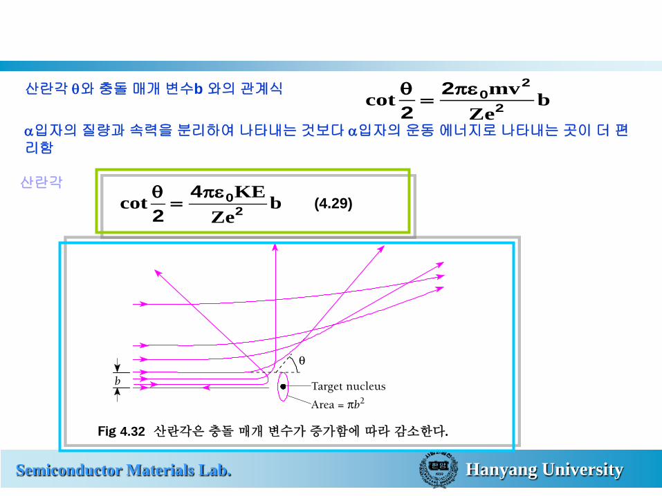
산란각 θ와 충돌 매개 변수b 와의 관계식 b
Zemvcot 2
202
2πε
=θ
α입자의 질량과 속력을 분리하여 나타내는 것보다 α입자의 운동 에너지로 나타내는 곳이 더 편리함
bZe
KEcot 204
2πε
=θ
(4.29) 산란각
Fig 4.32 산란각은 충돌 매개 변수가 증가함에 따라 감소한다.

Semiconductor Materials Lab. Hanyang University
B가 커짐에 따라 θ가 급속히 줄어드는 것이 명백히 나타나 있다 . 크게 굴절되기 위해서는 아주 가까이 입사해야 함
Rutherford 산란 공식
Eq4.29를 직접적으로 실험과 비교 할 수 없다
특정의 산란각에 해당하는 충돌 매개 변수를 측정할 방법이 없기 때문
θ는 eq4.29에 의해, b의 함수로 주어짐
핵의 중심으로 면적이 πb2인 원의 영역 안으로 입사한 α입자는 모두 각 θ 이거나 그 이상의 각으로 산란된다는 것을 의미함
면적 πb2을 상호작용의 단면적이라 부름. 단면적의 일반적인 기호 σ임.
단면적
입사하는 α입자는 실제로 핵의 바로 가장자리에 도달하기 전에 산란되기 시작 핵으로부터 b의 거리 안을 꼭 지날 필요는 없다
σ = π b2 (4.30)

Semiconductor Materials Lab. Hanyang University
단면적 A에 입사한 α입자의 전체 수와 그 중에서 각 θ 이상의 각도로 산란되는 입자의 비율 f는 그와 같은 산란이 생기게 하기 위한 단면적의 총합 ntAσ와 표적의 전체 면적 A의 비와 같다
입자입사된입자산란되는각으로이상의
ααθ
=
f
2bntA
ntA
π=
σ==
면적표적총합단면적의
Eq4.30을 이용해서 b를 치환하면
2422
0
2 θπε
π= cot)KE
Ze(ntf (4.31)
박막이 충분히 얇아서 인접한 핵의 단면적이 서로 겹치지 않고 산란된 α입자는 하나의 핵에 의해서 휘어질 만큼 완전히 휘어진다는 가정을 함

Semiconductor Materials Lab. Hanyang University
실제 실험에서는 θ 와 +dθ 사이로 산란되는 α입자를 측정기로 측정하게 된다
각 사이로 산란되는 α입자의 비율은 eq4.31을 θ에 대해 미분하면 얻을 수 있다
θθθ
πεπ−= dcsccot)
KEZe(ntdf
22422
0
2
(4.32)
음의 부호는 θ가 증가함에 따라 f가 감소함을 나타냄
Rutherford scattering formula
)(sinKEr)(
entZN)(N i
28 4222
0
42
θπε
=θ (4.1)

Semiconductor Materials Lab. Hanyang University
fig 4.33 러더퍼드(Rutherford)실험에서는 θ와 θ + d θ 사이로 산란된 입자를 검출한다.