2006 carts scintillation testing of electrolytic capacitors carts... · scintillation testing of...
TRANSCRIPT
©2006 Components Technology Institute, Inc., Huntsville, AL / 2006 CARTS Conference Proceedings, April 2006, Orlando, FL Page 1 of 7
Scintillation Testing of Solid Electrolytic Capacitors John D. Prymak 1, Mike Prevallet 2
KEMET Electronics Corp. PO Box 5928, Greenville, SC 29606
1-864-963-6300 (Phone) / 1-864-967-6876 (FAX) [email protected] 1 / [email protected] 2 (Email)
Abstract Self-healing is a phenomenon that has been presented in many discussions of the solid-state tantalum, niobium, and aluminum electrolytic capacitors. In these instances, the cathode material in contact with the dielectric of these ca-pacitors possesses a capability of changing the connection to the fault site of the dielectric. With the MnO2 cathode systems, it has been presented that this material gives up oxygen, and changes to a lower oxide state for this pair of elements, and in so doing changes the conductivity associated with the contact to the fault site. For the newer con-ductive polymer devices, the self-healing activity involves a change in the conductivity to the fault site, or a break in the contact by evaporating the polymer - an action very similar to fuse activation. We will present these events we refer to as scintillation, as a captured electrical measurement, including the equipment, techniques, and analysis of these scintillations. We will include additional capabilities of this measurement to define capacitance, leakage, and energy of scintillation capabilities with this measurement technique. We will show how the energy of scintillation is related to the cathode materials and how scintillation is an indicator of the quality of the dielectric.
Voltage Created Fault The fault avalanche or collapse is not due to the current, but is related to the voltage stress on the dielectric. The ca-pacitor’s dielectric is an insulator, and when it fails, it reverts to its opposite characteristic or becomes conductive. The higher sporadic current does not create the defect, but is a secondary catalyst that may push the dielectric break-down into an ignition mode. The failure is not the result of a poor conductive path for the plates, it is the dielectric, which breaks down and collapses. Its primary activation is by voltage stress, and not because of localized current constriction. Eliminating the current does not eliminate all failures, only the method of presentation of these fail-ures, to the outside observer.
Yet adding series resistance to the circuit does seem to eliminate the number of reported tantalum failures. The fail-ure totals noted in a circuit with significant resistance can appear to support the claim that the failures are not only less catastrophic in higher resistance circuits, but the numbers of reported failures can be found to be significantly lower. This testing has led many to believe that the higher current related to the lower resistances are responsible for increasing the failures.
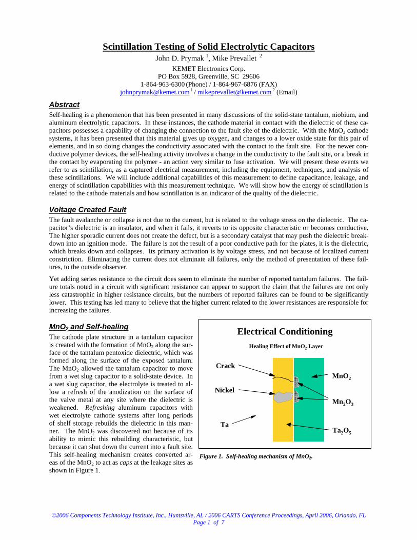
MnO2 and Self-healing The cathode plate structure in a tantalum capacitor is created with the formation of MnO2 along the sur-face of the tantalum pentoxide dielectric, which was formed along the surface of the exposed tantalum. The MnO2 allowed the tantalum capacitor to move from a wet slug capacitor to a solid-state device. In a wet slug capacitor, the electrolyte is treated to al-low a refresh of the anodization on the surface of the valve metal at any site where the dielectric is weakened. Refreshing aluminum capacitors with wet electrolyte cathode systems after long periods of shelf storage rebuilds the dielectric in this man-ner. The MnO2 was discovered not because of its ability to mimic this rebuilding characteristic, but because it can shut down the current into a fault site. This self-healing mechanism creates converted ar-eas of the MnO2 to act as caps at the leakage sites as shown in Figure 1.
Figure 1. Self-healing mechanism of MnO2.
Electrical ConditioningHealing Effect of MnO2 Layer
Crack
Nickel
TaTa2O5
MnO2
Mn2O3
©2006 Components Technology Institute, Inc., Huntsville, AL / 2006 CARTS Conference Proceedings, April 2006, Orlando, FL Page 2 of 7
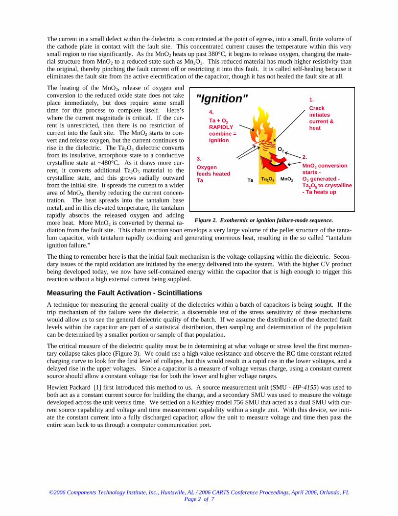
The current in a small defect within the dielectric is concentrated at the point of egress, into a small, finite volume of the cathode plate in contact with the fault site. This concentrated current causes the temperature within this very small region to rise significantly. As the MnO2 heats up past 380°C, it begins to release oxygen, changing the mate-rial structure from MnO2 to a reduced state such as Mn2O3. This reduced material has much higher resistivity than the original, thereby pinching the fault current off or restricting it into this fault. It is called self-healing because it eliminates the fault site from the active electrification of the capacitor, though it has not healed the fault site at all.
The heating of the MnO2, release of oxygen and conversion to the reduced oxide state does not take place immediately, but does require some small time for this process to complete itself. Here’s where the current magnitude is critical. If the cur-rent is unrestricted, then there is no restriction of current into the fault site. The MnO2 starts to con-vert and release oxygen, but the current continues to rise in the dielectric. The Ta2O5 dielectric converts from its insulative, amorphous state to a conductive crystalline state at ~480°C. As it draws more cur-rent, it converts additional Ta2O5 material to the crystalline state, and this grows radially outward from the initial site. It spreads the current to a wider area of MnO2, thereby reducing the current concen-tration. The heat spreads into the tantalum base metal, and in this elevated temperature, the tantalum rapidly absorbs the released oxygen and adding more heat. More MnO2 is converted by thermal ra-diation from the fault site. This chain reaction soon envelops a very large volume of the pellet structure of the tanta-lum capacitor, with tantalum rapidly oxidizing and generating enormous heat, resulting in the so called “tantalum ignition failure.”
The thing to remember here is that the initial fault mechanism is the voltage collapsing within the dielectric. Secon-dary issues of the rapid oxidation are initiated by the energy delivered into the system. With the higher CV product being developed today, we now have self-contained energy within the capacitor that is high enough to trigger this reaction without a high external current being supplied.
Measuring the Fault Activation - Scintillations A technique for measuring the general quality of the dielectrics within a batch of capacitors is being sought. If the trip mechanism of the failure were the dielectric, a discernable test of the stress sensitivity of these mechanisms would allow us to see the general dielectric quality of the batch. If we assume the distribution of the detected fault levels within the capacitor are part of a statistical distribution, then sampling and determination of the population can be determined by a smaller portion or sample of that population.
The critical measure of the dielectric quality must be in determining at what voltage or stress level the first momen-tary collapse takes place (Figure 3). We could use a high value resistance and observe the RC time constant related charging curve to look for the first level of collapse, but this would result in a rapid rise in the lower voltages, and a delayed rise in the upper voltages. Since a capacitor is a measure of voltage versus charge, using a constant current source should allow a constant voltage rise for both the lower and higher voltage ranges.
Hewlett Packard [1] first introduced this method to us. A source measurement unit (SMU - HP-4155) was used to both act as a constant current source for building the charge, and a secondary SMU was used to measure the voltage developed across the unit versus time. We settled on a Keithley model 756 SMU that acted as a dual SMU with cur-rent source capability and voltage and time measurement capability within a single unit. With this device, we initi-ate the constant current into a fully discharged capacitor; allow the unit to measure voltage and time then pass the entire scan back to us through a computer communication port.
Figure 2. Exothermic or ignition failure-mode sequence.
"Ignition"
Ta Ta2O5 MnO2
2.MnO2 conversionstarts - O2 generated -Ta2O5 to crystalline- Ta heats up
O2
3.Oxygenfeeds heatedTa
1.Crackinitiatescurrent &heat
4.Ta + O2RAPIDLYcombine =Ignition

©2006 Components Technology Institute, Inc., Huntsville, AL / 2006 CARTS Conference Proceedings, April 2006, Orlando, FL Page 3 of 7
We would like the unit to fully charge to the desired or compliance voltage in 10 to 12 seconds, and observe the results for a brief time span extending beyond this. Once the compliance voltage is reached, the constant current immediately drops to a lower level to “main-tain” the compliance voltage level. A scintillation will appear as a momentary drop in the voltage, and if the self-healing is successful, the voltage will then con-tinue to ramp back up (Figure 3). In order to achieve this span, the constant current was modified based on the capacitance: the larger the capacitance of the test unit, the higher the constant current was needed to achieve this 12 to 15 second window. The Keithley test unit appears to create a dual charge nature when the currents are well in excess of 1500 uA, such that the initial charge is at a higher current rate initially. This dual nature creates a sudden jump in the voltage across the capacitor, and then the expected slower rate. Since the higher capacitance requiring the higher currents are all of lower rated voltages, this sudden step hides any observable scintillation in the lower voltages that are important for these devices. As such, the span is selected such that either the current is selected to achieve a 15-second rise to compliance, or the current is limited to 1500 uA (thus creating spans of much longer duration than 15 seconds do).
Scintillations – Multiple Occurrences The scintillations are captured as the piece builds up charge and voltage stress by the SMU measured at fixed time intervals. Although multiple scintillations may be recorded, the first scintillation gives us an in-dication of the primary dielectric capability. Secon-dary scintillations can be generated in newly created fault sites immediately adjacent to the initial. We view these as a resultant of the primary fault, instead of existing before the primary. It makes sense that these sites should be detected in ever increasing stress levels. If a subsequent voltage level activates a scintillation below the level of a previous scintilla-tion, then that fault site must have been created after the activation of a previous scintillation.
Secondary scintillations can have stress levels much lower than the initial. In Figure 4, we tested a 50 volt rated unit of 10 uF to a compliance voltage of 300 VDC (6 x rated). Because the current to attain this voltage in 10 to 12 seconds would have been > 150 uA, 150 uA was chosen as the constant current and the time to attain the com-pliance voltage would have been near 22 seconds. As soon as the voltage rose to 110 VDC, the dielectric collapsed and some energy was utilized in heat to convert the MnO2. Because this fault site was healed, the voltage starts to rise again, but collapses a second time when it reaches just above 75 VDC. We do believe that the 75 VDC failure site did not exist during the initial ramp, or would have created a collapse at that point during the initial rise. It was created as a secondary effect to the enormous heat burst associated with the healing of the primary site. The rating or scintillation voltage rating for this device would have been 110 VDC.
The unit tested with the display recorded as in Figure 5, does show that each subsequent scintillation occurs at a higher voltage than any of the preceding scintillations. The initial failure occurs at 40 VDC, followed by scintilla-tions at 42, 90, and finally at 118 VDC. The fact that this unit fails as one might expect for different sites within the device, no such certainty can be concluded. For all we know, all four scintillations may have occurred at the exact same site. The only thing we can say for certain is that that first site had no assist. It was there within the unit prior to electrification created by this test.
Figure 3. Scintillation ramp and compliance.
Scintillation Testing
Time (seconds)
Volta
ge
Self-healing"Scintillation"
Compliance Voltage
Scintillation Voltage
Start
Figure 4. Multiple scintillations occurring for single piece.

©2006 Components Technology Institute, Inc., Huntsville, AL / 2006 CARTS Conference Proceedings, April 2006, Orlando, FL Page 4 of 7
We can estimate the energy utilized in the conver-sion process by calculating the energy levels before and after the scintillation (½CV2). From Figure 4, the energy changes are 60 millijoules (mj), 28 mj, and 19 mj. For Figure 5, the energy changes are 5 mj, 8 mj, 35 mj, and 71 mj. This evaluation may point out the severity of the fault, but it has to be relational to the voltage at which it breaks down. The only way to effectively compare these energy levels would be for the same units at the same scin-tillation level. Multiple energy levels dictated by multiple scintillations do offer an effective com-parison but this comparison is looking at the unper-turbed initial site and secondary sites that may have been compromised.
The scintillations do not always heal. After each of the occurrences with the first two pieces, there was always a rising voltage immediately after it reached some minimum point. Figure 6 shows where the second scintillation occurs and the sequence fol-lowing shows that the voltage is clamped at 12 VDC and is not rising. With this unit, the dielec-tric is no longer insulative. Based on 12 VDC with 150 uA of current, the resistance of this dielectric has changed from multiple Megohms, down to 80,000 ohms. Though this resistance may seem to be high, to a capacitor manufacturer it is as bad as a dead short.
With most scintillation, the results are not break-down. In many cases, the scintillations eventually get to the compliance voltage, but this level is cho-sen to get a reasonable majority of the pieces to fail. We initially chose 4x rated, but with the lower voltage units, this was not getting 90% of them failing. We wanted a higher percentage to fail to allow us more points to plot to establish a higher probability in our projections. We did experiment with 6x rated, as in these plots, but now we choose the compliance at 4x rated and accept the consequences.
Weibull Treatment of Data Let me point out that when these types of failure usually occur they appear as a subtle or nuisance problem for our customers, the failure rates will be in the tens of PPM or lower. The failures may appear and then disappear. These failures are heavily influenced by solder processes [3]. When they occur at higher rates, they move into serious problem categories that demand our full attention. The scintillation testing is a destructive test (We test to 4 or 6 times rated voltage to ensure failure.). In order to establish the resolution of the hundreds to the thousands of PPM levels, we would have to test thousands of pieces per batch. Our earlier exposure to this test relegated the results to a percentage tested that scintillated below the rated or the application voltage level. We soon found that there are many cases of samples with no pieces scintillating below the rated voltage of the part [2]. This summary was leav-ing too many lots with no discernable weakness detected with this analysis.
We then tried to utilize some statistical projections with this data. If we take the scintillation levels of the test sam-ples, order them, then look at a Weibull plot of cumulative percentage failures versus the voltage stress levels, we end up with charts looking like that of Figure 7.
In most cases, there is a distinct bi-modal effect apparent in the data distribution. Here we see that we can fit a line that encompasses the lower 9 points with some acceptable approximation of points encompassed within the lower
Figure 5. Increasing voltage levels with successive scintillations
Figure 6. Scintillation and dielectric breakdown.

©2006 Components Technology Institute, Inc., Huntsville, AL / 2006 CARTS Conference Proceedings, April 2006, Orlando, FL Page 5 of 7
group. This is the subjective part of this test, and in some cases, there are no questions as to consen-sus, but there are many distributions where the op-erators’ judgments do influence the results.
The operator can select a group from the lower three points, and points that are progressively higher. The program was written to allow the op-erator to use a horizontal scroll bar to stretch the inclusion group from the third point upwards. There is no allowance for eliminating the lowest points, and the fit must be to at least 3 points. Of paramount importance from these plots is the fail-ure rate at the application voltage or any voltage below that level. The program produces the 10%, 25%, 50%, 75% and 100% of rated voltage levels, and the operator can enter any voltage levels (up to 3) as might be required. The results from the above plot are not good. It projects a failure rate of 2.52% at the 50% rated voltage level. Ideally, this projection should be in the low PPM range. Also, the 100 PPM level (voltage level at which 100
PPM failure rate occur) should be higher than the rated voltage of the part, and with this sample, it shows it to be 1.75 VDC (3.5% of rated).
In Figure 8, the results are very good in that the 100 PPM level is at 49.3 VDC, or 140% of the rated. The 50% and 75% of rated voltage levels show predicted failure rates less than 1 PPM, with the 100% of rated showing a 1-PPM failure rate. Almost all the data points are used to establish the fit line.
No Scintillation or Leakage Testing these devices to 4x or 6x of rated voltage does not always assure that scintillation will occur. Consider the unit being tested in Figure 9 where the constant current is at 150 uA. Now the piece is rated at 35 VDC and the compliance voltage is set to 210 VDC (6x rated). The leakage requirement for this device would be 12 uA at 35 VDC. In Fig-ure 9, he voltage ceases to increase much beyond 74 VDC. This is because at 75 VDC, the leakage is very close to 150 uA. Compliance voltage is never reached, and no sudden drops in voltage (scintillations) are de-tected. This piece shows no scintillations.
Capacitance and Leakage Measurements From the earliest portion of the curve (the first ten data points) the dv/dt is used with the constant current to calculate the capacitance of the test unit. This measurement assumes that there is no leakage current at these very small volt-ages, and all of the charging current is creating a cumulative charge (dv).
This capacitance at a constant current should maintain that charging slope continuously, but as the voltage is in-creasing, the leakage current is also increasing. The leakage current steals from the charging current to the point where the dv/dt slope near rated voltage is now lower than that measured with the first 10 readings. By calculating the changed slope, the new charging current can be calculated and the difference between this charging current and
Figure 7. Statistical treatment of cumulative failure data.
Figure 8. Good results from scintillation test.

©2006 Components Technology Institute, Inc., Huntsville, AL / 2006 CARTS Conference Proceedings, April 2006, Orlando, FL Page 6 of 7
the initial dv/dt is the leakage current. For this de-vice shown in Figure 9, the calculated leakage is 7.8 uA, well below the 12-uA catalog limit.
As the voltage increases, multiple leakage sites start to conduct more current. Each site does not have enough heat generated to convert the MnO2 in this short time frame. As the voltage increases, more leakage sites are turned on, and the current through the previous sites increases. The voltage reaches a level of about 74 VDC and at this point, the total leakage for all conducting sites is equal to the 150 uA of constant current – no increases in voltage are apparent.
Clearing ‘Shorts’ There are instances in this testing where the fault appears to create a ‘short’ condition, and then par-tially of full recover. In Figure 10, the plot on the right shows that the device appears to fail catastrophically. The current (even though it is only 150 uA) continues pumping energy into the part, and physical disruption from the broiling mass appears to then create an ‘open’ condi-tion. This clearing effect may not result in an ‘open’ condition; but, it can lead to a increasing resistance with time as the device cools. This cooling and increasing resistance with time is shown on the left in Figure 10. Although this device does not have the breakdown condition it had in its original charge, it does have a range through 10 VDC that it again appears as capacitive.
The results in the left plot of Figure 10 point out why measuring resistance of the failed unit after some time may not be indicative of the high conductivity created by the device immediately after failure. If the part cools, then the mol-ten high conductivity of the materials within are allowed to solidify and contract, creating breaks in the ‘shorted’ paths created at the time of failure.
Figure 9. High leakage equals constant current – voltage clamped.
Figure 10. Apparent recovery of ‘short’ to higher resistance (left) and ‘open’ (right).
©2006 Components Technology Institute, Inc., Huntsville, AL / 2006 CARTS Conference Proceedings, April 2006, Orlando, FL Page 7 of 7
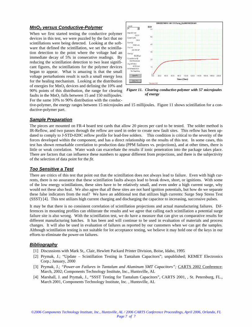
MnO2 versus Conductive-Polymer When we first started testing the conductive polymer devices in this test, we were puzzled by the fact that no scintillations were being detected. Looking at the soft-ware that defined the scintillation, we set the scintilla-tion detection to the point where the voltage had an immediate decay of 5% in consecutive readings. By reducing the scintillation detection to two least signifi-cant figures, the scintillations for the polymer devices began to appear. What is amazing is that the small voltage perturbations result is such a small energy loss for the healing mechanism. Looking at the distribution of energies for MnO2 devices and defining the 10% and 90% points of this distribution, the range for clearing faults in the MnO2 falls between 15 and 150 millijoules. For the same 10% to 90% distribution with the conduc-tive-polymer, the energy ranges between 15 microjoules and 15 millijoules. Figure 11 shows scintillation for a con-ductive-polymer part.
Sample Preparation The pieces are mounted on FR-4 board test cards that allow 20 pieces per card to be tested. The solder method is IR-Reflow, and two passes through the reflow are used in order to create new fault sites. This reflow has been up-dated to comply to J-STD-020C reflow profile for lead-free solders. This condition is critical to the severity of the forces developed within the component, and has a direct relationship on the results of this test. In some cases, this test has shown remarkable correlation to production data (PPM failures vs. projections), and at other times, there is little or weak correlation. Water wash can exacerbate the results if ionic penetration into the package takes place. There are factors that can influence these numbers to appear different from projections, and there is the subjectivity of the selection of data point for the fit.
Too Sensitive a Test There are critics of this test that point out that the scintillation does not always lead to failure. Even with high cur-rents, there is no assurance that these scintillation faults always lead to break down, short, or ignitions. With some of the low energy scintillations, these sites have to be relatively small, and even under a high current surge, why would not these also heal. We also agree that all these sites are not hard ignition potentials, but how do we separate these false indicators from the real? We have an additional test that utilizes high currents: Surge Step Stress Test (SSST) [4]. This test utilizes high current charging and discharging the capacitor to increasing, successive pulses.
It may be that there is no consistent correlation of scintillation projections and actual manufacturing failures. Dif-ferences in mounting profiles can obliterate the results and we agree that calling each scintillation a potential surge failure site is also wrong. With the scintillation test, we do have a measure that can give us comparative results for different manufacturing batches. It has been and will continue to be used in evaluation of materials and process changes. It will also be used in evaluation of failures as reported by our customers when we can get the samples. Although scintillation testing is not suitable for lot acceptance testing, we believe it may hold one of the keys in our efforts to eliminate the power-on failures.
Bibliography [1] Discussions with Mark St,. Clair, Hewlett Packard Printer Division, Boise, Idaho, 1995 [2] Prymak, J.; “Update – Scintillation Testing in Tantalum Capacitors”; unpublished; KEMET Electronics
Corp.; January, 2000 [3] Prymak, J.; “Power-on Failures in Tantalum and Aluminum SMT Capacitors”; CARTS 2002 Conference;
March, 2002; Components Technology Institute, Inc., Huntsville, AL [4] Marshall, J. and Prymak, J., “SSST Testing for Tantalum Capacitors”, CARTS 2001, , St. Petersburg, FL.,
March 2001, Components Technology Institute, Inc. , Huntsville, AL
Figure 11. Clearing conductive-polymer with 57 microjoules of energy