16-channel, 16-bit analog-to-digital converter (rev. d)
TRANSCRIPT

ADS1158
16-Bit
ADC
Digital
Filter
Internal
Monitoring
16:1
Analog
Input
MUX
1
16
AINCOM
¼
ADC
IN
Ext CLK
In/Out
AVSS DGND32.768kHz
AVDD DVDD
MUX
OUT
SPI
Interface
CS
DRDYSCLK
DIN
DOUT
ControlOscillator
GPIO
START
RESET
PWDN
GPIO[7:0]VREF
ADS1158
Analog Inputs
ADS1158
www.ti.com SBAS429D –JUNE 2008–REVISED MARCH 2011
16-Channel, 16-Bit Analog-to-Digital ConverterCheck for Samples: ADS1158
1FEATURES DESCRIPTIONThe ADS1158 is a 16-channel (multiplexed),
23• 16 Bits, No Missing Codeslow-noise, 16-bit, delta-sigma (ΔΣ) analog-to-digital• Fixed-Channel or Automatic Channel Scan converter (ADC) that provides single-cycle settled
• Fixed-Channel Data Rate: 125kSPS data at channel scan rates from 1.8k to 23.7ksamples per second (SPS) per channel. A flexible• Auto-Scan Data Rate: 23.7kSPS/Channelinput multiplexer accepts combinations of eight• Single-Conversion Settled Data differential or 16 single-ended inputs with a full-scale
• 16 Single-Ended or 8 Differential Inputs differential range of 5V or true bipolar range of ±2.5Vwhen operating with a 5V reference. The fourth-order• Unipolar (+5V) or Bipolar (±2.5V) Operationdelta-sigma modulator is followed by a fifth-order sinc• 0.3LSB (INL)digital filter optimized for low-noise performance.
• DC Stability:The differential output of the multiplexer is accessible1μV/°C Offset Drift, 2ppm/°C Gain Driftto allow signal conditioning before the input of the• Open-Sensor Detection ADC. Internal system monitor registers provide
• Conversion Control Pin supply voltage, temperature, reference voltage, gain,and offset data.• Multiplexer Output for External Signal
Conditioning An onboard PLL generates the system clock from a32.768kHz crystal, or can be overridden by an• On-Chip Temperature, Reference, Offset, Gain,external clock source. A buffered system clock outputand Supply Voltage Readback(15.7MHz) is provided to drive a microcontroller or• 42mW Power Dissipationadditional converters.
• Standby, Sleep, and Power-Down ModesSerial digital communication is handled via an• Eight General-Purpose Inputs/Outputs (GPIO) SPI™-compatible interface. A simple command word
• 32.768kHz Crystal Oscillator or External Clock structure controls channel configuration, data rates,digital I/O, monitor functions, etc.
APPLICATIONSProgrammable sensor bias current sources can be
• Medical, Avionics, and Process Control used to bias sensors or verify sensor integrity.• Machine and System Monitoring The ADS1158 operates from a unipolar +5V or• Fast Scan Multi-Channel Instrumentation bipolar ±2.5V analog supply and a digital supply
compatible with interfaces ranging from 2.7V to• Industrial Systems5.25V. The ADS1158 is available in a QFN-48• Test and Measurement Systemspackage.
1
Please be aware that an important notice concerning availability, standard warranty, and use in critical applications of TexasInstruments semiconductor products and disclaimers thereto appears at the end of this data sheet.
2SPI is a trademark of Motorola, Inc.3All other trademarks are the property of their respective owners.
PRODUCTION DATA information is current as of publication date. Copyright © 2008–2011, Texas Instruments IncorporatedProducts conform to specifications per the terms of the TexasInstruments standard warranty. Production processing does notnecessarily include testing of all parameters.

ADS1158
SBAS429D –JUNE 2008–REVISED MARCH 2011 www.ti.com
This integrated circuit can be damaged by ESD. Texas Instruments recommends that all integrated circuits be handled withappropriate precautions. Failure to observe proper handling and installation procedures can cause damage.
ESD damage can range from subtle performance degradation to complete device failure. Precision integrated circuits may be moresusceptible to damage because very small parametric changes could cause the device not to meet its published specifications.
ORDERING INFORMATION
For the most current package and ordering information see the Package Option Addendum at the end of thisdocument, or see the TI web site at www.ti.com.
ABSOLUTE MAXIMUM RATINGSOver operating free-air temperature range, unless otherwise noted. (1)
ADS1158 UNIT
AVDD to AVSS –0.3 to +5.5 V
AVSS to DGND –2.8 to +0.3 V
DVDD to DGND –0.3 to +5.5 V
Input current 100, momentary mA
Input current 10, continuous mA
Analog input voltage AVSS – 0.3 to AVDD + 0.3 V
Digital input voltage to DGND –0.3 to DVDD + 0.3 V
Maximum junction temperature +150 °COperating temperature range –40 to +105 °CStorage temperature range –60 to +150 °C
(1) Stresses above these ratings may cause permanent damage. Exposure to absolute maximum conditions for extended periods maydegrade device reliability. These are stress ratings only, and functional operation of the device at these or any other conditions beyondthose specified is not implied.
2 Submit Documentation Feedback Copyright © 2008–2011, Texas Instruments Incorporated
Product Folder Link(s): ADS1158

ADS1158
www.ti.com SBAS429D –JUNE 2008–REVISED MARCH 2011
ELECTRICAL CHARACTERISTICSAll specifications at TA = –40°C to +105°C, AVDD = +2.5V, AVSS = –2.5V, DVDD = +3.3V, fCLK = 16MHz (external clock) or fCLK =15.729MHz (internal clock), OPA227 buffer between MUX outputs and ADC inputs, VREF = +4.096V, and VREFN = –2.5V, unless otherwisenoted.
ADS1158
PARAMETER CONDITIONS MIN TYP MAX UNIT
ANALOG MULTIPLEXER INPUTS
AIN0–AIN15,Absolute input voltage AVSS – 100mV AVDD + 100mV VAINCOM with respect to DGND
On-channel resistance 80 Ω
Crosstalk fIN = 1kHz –110 dB
SBCS[1:0] = 01 1.5Sensor bias (current source) μA
SBCS[1:0] = 11 24
1.5μA:24μA ratio error 1 %
ADC INPUT
Full-scale input voltage (VIN = ADCINP – ADCINN) ±1.06 VREF V
Absolute input voltage (ADCINP, ADCINN) AVSS – 100mV AVDD + 100mV V
Differential input impedance 65 kΩ
SYSTEM PERFORMANCE
Resolution No missing codes 16 Bits
Data rate, fixed-channel mode 1.953 125 kSPS
Data rate, auto-scan mode 1.805 23.739 kSPS
Integral nonlinearity (INL) (1) Differential input 0.3 1 LSB (2)
Offset error Chopping on Shorted inputs –1 –0.5 (3) 0 LSB
Offset drift Shorted inputs 1 μV/°C
Gain error 0.1 0.5 %
Gain drift 2 ppm/°C
Noise 0.6 LSB (PP)
Common-mode rejection fCM = 60Hz 100 dB
AVDD, AVSS 85Power-supply rejection fPS = 60Hz dB
DVDD 95
VOLTAGE REFERENCE INPUT
Reference input voltage (VREF = VREFP – VREFN) 0.5 4.096 AVDD – AVSS V
Negative reference input (VREFN) AVSS – 0.1V VREFP – 0.5 V
Positive reference input (VREFP) VREFN + 0.5 AVDD + 0.1V V
Reference input impedance 40 kΩ
SYSTEM PARAMETERS
External reference reading error 1 3 %
Analog supply reading error 1 5 %
Voltage TA = +25°C 168 mV
Temperature sensor reading 394 (4) μV/°CCoefficient
563 (5) μV/°C
(1) Best straight line fit method.(2) FSR = Full-scale range = 2.13VREF.(3) Systematic –0.5LSB in reading code.(4) ADS1158 temperature forced alone, test PCB in free air.(5) ADS1158 and test PCB temperatures forced together.
Copyright © 2008–2011, Texas Instruments Incorporated Submit Documentation Feedback 3
Product Folder Link(s): ADS1158

ADS1158
SBAS429D –JUNE 2008–REVISED MARCH 2011 www.ti.com
ELECTRICAL CHARACTERISTICS (continued)All specifications at TA = –40°C to +105°C, AVDD = +2.5V, AVSS = –2.5V, DVDD = +3.3V, fCLK = 16MHz (external clock) orfCLK = 15.729MHz (internal clock), OPA227 buffer between MUX outputs and ADC inputs, VREF = +4.096V, and VREFN= –2.5V, unless otherwise noted.
ADS1158
PARAMETER CONDITIONS MIN TYP MAX UNIT
DIGITAL INPUT/OUTPUT
VIH 0.7DVDD DVDD V
VIL DGND 0.3DVDD VLogic levels
VOH IOH = 2mA 0.8DVDD DVDD V
VOL IOL = 2mA DGND 0.2DVDD V
Input leakage VIN = DVDD, GND 10 μA
Frequency 0.1 16 MHzMaster clock input (CLKIO)
Duty cycle 40 60 %
Crystal frequency 32.768 kHz
Clock output frequency 15.729 MHzCrystal oscillator(see Crystal Oscillator section) Start-up time (clock output valid) 150 ms
Clock output duty cycle 40 60 %
POWER SUPPLY
DVDD 2.7 5.25 V
AVSS –2.6 0 V
AVDD AVSS + 4.75 AVSS + 5.25 V
External clock 0.25 0.6 mAoperation
Internal oscillatoroperation, clock 0.04 mAoutput disabledDVDD supply current
Internal oscillatoroperation, clock 1.4 mA
output enabled (6)
Power-down (7) 1 25 µA
Converting 8.2 12 mA
Standby 5.6 mAAVDD, AVSS supply current
Sleep 2.1 mA
Power-down 2 200 µA
Converting 42 62 mW
Standby 29 mWPower dissipation
Sleep 11 mW
Power-down 14 μW
(6) CLKIO load = 20pF.(7) No clock applied to CLKIO.
4 Submit Documentation Feedback Copyright © 2008–2011, Texas Instruments Incorporated
Product Folder Link(s): ADS1158

36
35
34
33
32
31
30
29
28
27
26
25
AIN12
AIN13
AIN14
AIN15
AINCOM
VREFP
VREFN
DGND
DVDD
CS
START
DRDY
AIN
4C
LK
IO
AIN
5G
PIO
0
AIN
6G
PIO
1
AIN
7G
PIO
2
MU
XO
UT
PG
PIO
3
MU
XO
UT
NG
PIO
4
AD
CIN
PG
PIO
5
AD
CIN
NG
PIO
6
AIN
8G
PIO
7
AIN
9S
CLK
AIN
10
DIN
AIN
11
DO
UT
1
2
3
4
5
6
7
8
9
10
11
12
AIN3
AIN2
AIN1
AIN0
AVSS
AVDD
PLLCAP
XTAL1
XTAL2
PWDN
RESET
CLKSEL
48 47 46 45 44 43 42 41 40 39 38
13 14 15 16 17 18 19 20 21 22 23
37
24
ADS1158
ADS1158
www.ti.com SBAS429D –JUNE 2008–REVISED MARCH 2011
PIN CONFIGURATION
QFN PACKAGE(TOP VIEW)
PIN ASSIGNMENTSANALOG/DIGITAL
PIN # NAME INPUT/OUTPUT DESCRIPTION
1 AIN3 Analog input Analog input 3: single-ended channel 3, differential channel 1 (–)
2 AIN2 Analog input Analog input 2: single-ended channel 2, differential channel 1 (+)
3 AIN1 Analog input Analog input 1: single-ended channel 1, differential channel 0 (–)
4 AIN0 Analog input Analog input 0: single-ended channel 0, differential channel 0 (+)
Negative analog power supply: 0V for unipolar operation, –2.5V for bipolar operation.5 AVSS Analog (Internally connected to exposed thermal pad of QFN package.)
6 AVDD Analog Positive analog power supply: +5V for unipolar operation, +2.5V for bipolar operation.
7 PLLCAP Analog PLL bypass capacitor: connect 22nF capacitor to AVSS when using crystal oscillator.
8 XTAL1 Analog 32.768kHz crystal oscillator input 1; see Crystal Oscillator section.
9 XTAL2 Analog 32.768kHz crystal oscillator input 2; see Crystal Oscillator section.
10 PWDN Digital input Power-down input: hold low for minimum of two fCLK cycles to engage low-power mode.
11 RESET Digital input Reset input: hold low for minimum of two fCLK cycles to reset the device.
Clock select input: Low = activates crystal oscillator, fCLK output on CLKIO.12 CLKSEL Digital input High = disables crystal oscillator, apply fCLK to CLKIO.
13 CLKIO Digital I/O System clock input/output (see CLKSEL pin)
14 GPIO0 Digital I/O General-purpose digital input/output 0
15 GPIO1 Digital I/O General-purpose digital input/output 1
16 GPIO2 Digital I/O General-purpose digital input/output 2
17 GPIO3 Digital I/O General-purpose digital input/output 3
18 GPIO4 Digital I/O General-purpose digital input/output 4
19 GPIO5 Digital I/O General-purpose digital input/output 5
20 GPIO6 Digital I/O General-purpose digital input/output 6
Copyright © 2008–2011, Texas Instruments Incorporated Submit Documentation Feedback 5
Product Folder Link(s): ADS1158

ADS1158
SBAS429D –JUNE 2008–REVISED MARCH 2011 www.ti.com
PIN ASSIGNMENTS (continued)ANALOG/DIGITAL
PIN # NAME INPUT/OUTPUT DESCRIPTION
21 GPIO7 Digital I/O General-purpose digital input/output 7
22 SCLK Digital input SPI interface clock input: data clocked in on rising edge, clocked out on falling edge.
23 DIN Digital input SPI interface data input: data are input to the device.
24 DOUT Digital output SPI interface data output: data are output from the device.
25 DRDY Digital output Data ready output: active low.
26 START Digital input Start conversion input: active high.
27 CS Digital input SPI interface chip select input: active low.
28 DVDD Digital Digital power supply: 2.7V to 5.25V
29 DGND Digital Digital ground
30 VREFN Analog input Reference input negative
31 VREFP Analog input Reference input positive
32 AINCOM Analog input Analog input common: common input pin to all single-ended inputs.
33 AIN15 Analog input Analog input 15: single-ended channel 15, differential channel 7 (–)
34 AIN14 Analog input Analog input 14: single-ended channel 14, differential channel 7 (+)
35 AIN13 Analog input Analog input 13: single-ended channel 13, differential channel 6 (–)
36 AIN12 Analog input Analog input 12: single-ended channel 12, differential channel 6 (+)
37 AIN11 Analog input Analog input 11: single-ended channel 11, differential channel 5 (–)
38 AIN10 Analog input Analog input 10: single-ended channel 10, differential channel 5 (+)
39 AIN9 Analog input Analog input 9: single-ended channel 9, differential channel 4 (–)
40 AIN8 Analog input Analog input 8: single-ended channel 8, differential channel 4 (+)
41 ADCINN Analog input ADC differential input (–)
42 ADCINP Analog input ADC differential input (+)
43 MUXOUTN Analog output Multiplexer differential output (–)
44 MUXOUTP Analog output Multiplexer differential output (+)
45 AIN7 Analog input Analog input 7: single-ended channel 7, differential channel 3 (–)
46 AIN6 Analog input Analog input 6 : single-ended channel 6, differential channel 3 (+)
47 AIN5 Analog input Analog input 5: single-ended channel 5, differential channel 2 (–)
48 AIN4 Analog input Analog input 4: single-ended channel 4, differential channel 2 (+)
6 Submit Documentation Feedback Copyright © 2008–2011, Texas Instruments Incorporated
Product Folder Link(s): ADS1158

SCLK
CS(1)
DIN
DOUT
tSCLKtCSSC
tSPW
tDIST
tDIHD
tSPW
tCSDO
Hi-ZHi-Z
tCSPW
tDOPD
tDOHD
DRDY
DOUT
tDRDY
tDDO
ADS1158
www.ti.com SBAS429D –JUNE 2008–REVISED MARCH 2011
PARAMETER MEASUREMENT INFORMATION
(1) CS can be tied low.
Figure 1. Serial Interface Timing
SERIAL INTERFACE TIMING CHARACTERISTICSAt TA= –40°C to +105°C and DVDD = 2.7V to 5.25V, unless otherwise noted.
SYMBOL DESCRIPTION MIN MAX UNITS
tSCLK SCLK period 2 τCLK(1)
tSPW SCLK high or low pulse width (exceeding max resets SPI interface) 0.8 4096 (2) τCLK
tCSSC CS low to first SCLK: setup time (3) 2.5 τCLK
tDIST Valid DIN to SCLK rising edge: setup time 10 ns
tDIHD Valid DIN to SCLK rising edge: hold time 5 ns
tDOPD SCLK falling edge to valid new DOUT: propagation delay (4) 20 ns
tDOHD SCLK falling edge to old DOUT invalid: hold time 0 ns
tCSDO CS high to DOUT invalid (3-state) 5 τCLK
tCSPW CS pulse width high 2 τCLK
(1) τCLK = master clock period = 1/fCLK.(2) Programmable to 256 τCLK.(3) CS can be tied low.(4) DOUT load = 20pF || 100kΩ to DGND.
Figure 2. DRDY Update Timing
DRDY UPDATE TIMING CHARACTERISTICSSYMBOL DESCRIPTION TYP UNITS
t DRDY DRDY high pulse width without data read 1 τCLK
tDDO Valid DOUT to DRDY falling edge (CS = 0) 0.5 τCLK
Copyright © 2008–2011, Texas Instruments Incorporated Submit Documentation Feedback 7
Product Folder Link(s): ADS1158

Nu
mb
er
of
Occu
rre
nce
s
Offset (Output Code)
6000
5000
4000
3000
2000
1000
0
-4 -3 3-2 -1 0 2
25 Units, 256 Samples/Unit
1
Nu
mb
er
of
Occu
rre
nce
s
Offset (Output Code)
3500
3000
2500
2000
1500
1000
500
0
-2 2-1 0 1
25 Units,
254 Samples/Unit
Norm
aliz
ed O
ffset (
V)
m
Temperature ( C)°
100
50
0
50
100
150
200
250
-
-
-
-
-
-40 -15 11010 60 8535
CHOP = 1
CHOP = 0
Nu
mb
er
of
Occu
rre
nce
s
Absolute Gain Error (ppm)
40
35
30
25
20
15
10
5
0
10
0
150 Units From Two Production Sets
20
00
11
00
14
00
13
00
12
00
15
00
90
0
10
00
17
00
60
0
30
0
40
0
50
0
20
0
80
0
70
0
16
00
18
00
19
00
Norm
aliz
ed
Gain
Err
or
(ppm
)
Temperature ( C)°
60
40
20
0
20
40
60
80
100
120
140
-
-
-
-
-
-
-
-40 -15 11010 60 8535
Num
ber
of O
ccurr
ences
Gain Drift (ppm/ C)°
30
25
20
15
10
5
0
-3.8
150 Units From Two Production Sets
0.3
1.5
0.9
2.1
-0.3
-3.3
-2.7
-2.1
-0.9
-1.5
2.7
3.3
3.8
ADS1158
SBAS429D –JUNE 2008–REVISED MARCH 2011 www.ti.com
TYPICAL CHARACTERISTICSAt TA = +25°C, AVDD = +2.5V, AVSS = –2.5V, DVDD = +3.3V, fCLK = 16MHz (external clock) or fCLK = 15.729MHz (internal clock), OPA227buffer between MUX outputs and ADC inputs, VREFP = +2.048V, and VREFN = –2.048V, unless otherwise noted.
OFFSET WITH 0.5V REFERENCE, CHOPPING ON OFFSET WITH 4.096V REFERENCE, CHOPPING ON
Figure 3. Figure 4.
OFFSET vs TEMPERATURE GAIN ERROR HISTOGRAM
Figure 5. Figure 6.
GAIN DRIFT HISTOGRAM GAIN ERROR vs TEMPERATURE
Figure 7. Figure 8.
8 Submit Documentation Feedback Copyright © 2008–2011, Texas Instruments Incorporated
Product Folder Link(s): ADS1158

Lin
earity
Err
or
(ppm
)
V (V)REF
10
9
8
7
6
5
4
3
2
1
00.5 1.0 5.01.5 2.5 3.02.0 4.54.03.5
Lin
earity
Err
or
(ppm
)
V (V)IN
8
6
4
2
0
2
4
6
8
-
-
-
-
-5 -4 5-3 -1 0-2 321 4
T = +25 C°A
T = 10 C- °A
T = 40 C- °A
T = +105 C°A
T = +85 C°A
T = +55 C°A
V = 4.096VREF
INL (
ppm
)
Temperature ( C)°
7
6
5
4
3
2
1
0
-40 -15 11010 60 8535
Level(d
BF
S)
Frequency (Hz)
0
20
40
60
80
100
120
140
160
180
200
-
-
-
-
-
-
-
-
-
-
1 100k10 100 10k1k
f = 1kHz, 0.5dBFS
DRATE[1:0] = 11
32768 Points
-
Tem
pe
ratu
re S
en
so
rV
olta
ge
(m
V)
Temperature ( C)°
220
210
200
190
180
170
160
150
140
130
120
-40 -20 12020 60 80400 100
ADS1158 Only Temperature Forced,
Test PCB in Free Air
ADS1158 and Test PCB Temperatures
Forced Together
Nu
mb
er
of
Occu
rre
nce
s
Temperature Reading ( C)°
8
7
6
5
4
3
2
1
0
15
35 Units From Two Production Sets
22
24
23
2521
16
17
18
20
19
26
27
28
39
37
35
3331
29
38
36
34
32
30
ADS1158
www.ti.com SBAS429D –JUNE 2008–REVISED MARCH 2011
TYPICAL CHARACTERISTICS (continued)At TA = +25°C, AVDD = +2.5V, AVSS = –2.5V, DVDD = +3.3V, fCLK = 16MHz (external clock) or fCLK = 15.729MHz (internalclock), OPA227 buffer between MUX outputs and ADC inputs, VREFP = +2.048V, and VREFN = –2.048V, unless otherwisenoted.
INTEGRAL NONLINEARITY vs VREF INTEGRAL NONLINEARITY vs INPUT LEVEL
Figure 9. Figure 10.
INL vs TEMPERATURE OUTPUT SPECTRUM
Figure 11. Figure 12.
TEMPERATURE SENSOR VOLTAGE vs TEMPERATURE TEMPERATURE SENSOR READING HISTOGRAM
Figure 13. Figure 14.
Copyright © 2008–2011, Texas Instruments Incorporated Submit Documentation Feedback 9
Product Folder Link(s): ADS1158

Ratio (
A/
A)
mm
Temperature ( C)°
18.0
17.5
17.0
16.5
16.0
15.5
15.0
14.5
14.0
-40 -15 11010 60 8535
Nu
mb
er
of
Occu
rre
nce
s
Ratio ( A/ A)mm
14
12
10
8
6
4
2
0
14.0 19.015.5 17.0 18.0
25 Units From
One Production Lot
14.5 16.0 17.5 18.515.0 16.5
AV
DD
/AV
SS
Curr
ent (m
A)
Temperature ( C)°
10
8
6
4
2
0-40 -15 11010 60 8535
DVDD
AVDD/AVSS
DV
DD
Curre
nt (m
A)
1.0
0.8
6
4
2
0
0.
0.
0.
Cu
rre
nt
(A
)m
Temperature ( C)°
4
3
2
1
0
-40 -15 11010 60 8535
Unipolar
AVSS = 0V, AVDD = 5V
AVSS/AVDD
Cu
rre
nt
(A
)m
Temperature ( C)°
140
120
100
80
60
40
20
0
-40 -15 11010 60 8535
AVSS
AVDD
Bipolar
AVSS = 2.5V, AVDD = 2.5V-
ADS1158
SBAS429D –JUNE 2008–REVISED MARCH 2011 www.ti.com
TYPICAL CHARACTERISTICS (continued)At TA = +25°C, AVDD = +2.5V, AVSS = –2.5V, DVDD = +3.3V, fCLK = 16MHz (external clock) or fCLK = 15.729MHz (internalclock), OPA227 buffer between MUX outputs and ADC inputs, VREFP = +2.048V, and VREFN = –2.048V, unless otherwisenoted.
SENSOR BIAS CURRENT SOURCE RATIO vsSENSOR BIAS CURRENT SOURCE RATIO HISTOGRAM TEMPERATURE
Figure 15. Figure 16.
SUPPLY CURRENT vs TEMPERATURE POWER-DOWN CURRENT vs TEMPERATURE
Figure 17. Figure 18.
POWER-DOWN CURRENT vs TEMPERATURE
Figure 19.
10 Submit Documentation Feedback Copyright © 2008–2011, Texas Instruments Incorporated
Product Folder Link(s): ADS1158

AIN0
AIN1
AIN2
AIN3
AIN4
AIN5
AIN6
AIN7
AIN8
AIN9
AIN10
AIN11
AIN12
AIN13
AIN14
AIN15
AINCOM
Control
Logic
VREFPVREFNAVSS
PLLCAP XTAL1XTAL2
DRDY
PWDN
RESET
START
SPI
Interface
CS
SCLK
DIN
DOUT
Digital Filter
Clock Control
16-Channel
MUX
AVDD
Sensor
Bias
MUXOUTP MUXOUTN ADCINP GNDADCINN
ADC Channel Control
Supply Monitor
GPIO
GPIO[7:0]DVDD
Temperature
Ext Ref Monitor
Internal Ref
ADC
CLKSELCLKIO
ADS1158
www.ti.com SBAS429D –JUNE 2008–REVISED MARCH 2011
OVERVIEW
The ADS1158 is a flexible, 16-bit, low-noise ADC The ADS1158 converter consists of a fourth-order,optimized for fast multi-channel, high-resolution delta-sigma modulator followed by a programmablemeasurement systems. The converter provides a digital filter. The modulator measures the differentialmaximum channel scan rate of 23.7kSPS, giving a input signal, VIN = (ADCINP – ADCINN), against thecomplete 16-channel scan in less than 700μs. differential reference input, VREF = (VREFP –
VREFN). The digital filter receives the modulatorFigure 20 shows the block diagram of the ADS1158. signal and provides a low-noise digital output. TheThe input multiplexer selects which analog input pins ADC channel block controls the multiplexerconnect to the multiplexer output pins Auto-Scan feature. Channel Auto-Scan occurs at a(MUXOUTP/MUXOUTN). External signal conditioning maximum rate of 23.7kSPS. Slower scan rates cancan be used between the multiplexer output pins and be used with corresponding increases in resolution.the ADC input pins (ADCINP/ADCINN) or themultiplexer output can be routed internally to the ADC Communication is handled over an SPI-compatibleinputs without external circuitry. Selectable current serial interface with a set of simple commands tosources within the input multiplexer can be used to control the ADS1158. Onboard registers store thebias sensors or detect for a failed sensor. On-chip various settings for the input multiplexer, sensorsystem function readings provide readback of detect bias, data rate selection, etc. Either antemperature, supply voltage, gain, offset, and external external 32.768kHz crystal, connected to pins XTAL1reference. and XTAL2, or an external clock applied to pin CLKIO
can be used as the clock source. When using theexternal crystal oscillator, the system clock isavailable as an output for driving other devices orcontrollers. General-purpose digital I/Os (GPIO)provide input and output control of eight pins.
Figure 20. ADS1158 Block Diagram
Copyright © 2008–2011, Texas Instruments Incorporated Submit Documentation Feedback 11
Product Folder Link(s): ADS1158

ESD
Diodes
ESD
Diodes
3pF Reff = 40kW
(f = 16MHz)CLK
AVDD
AVSS
VREFP
VREFN
AVSS 100mV < (VREFP or VREFN) < AVDD + 100mV-
ADS1158
SBAS429D –JUNE 2008–REVISED MARCH 2011 www.ti.com
MULTIPLEXER INPUTS The load presented by the switched capacitor can bemodeled with an effective resistance (Reff) of 40kΩ for
A simplified diagram of the input multiplexer is fCLK = 16MHz. Note that the effective impedance ofillustrated in Figure 22. The multiplexer connects one the reference inputs loads an external reference withof 16 single-ended external inputs, one of eight a non-zero source impedance.differential external inputs, or one of the on-chipinternal variables to the ADC inputs. The output of thechannel multiplexer can be routed to external pinsand then to the input of the ADC. This flexibilityallows for use of external signal conditioning. See theExternal Multiplexer Loop section.
Electrostatic discharge (ESD) diodes protect theanalog inputs. To keep these diodes from turning on,make sure the voltages on the input pins do not gobelow AVSS by more than 100mV, and likewise donot exceed AVDD by more than 100mV:
AVSS – 100mV < (Analog Inputs) < AVDD + 100mV.
Overdriving the multiplexer inputs may affect theconversions of other channels. See the InputOverload Protection description in the HardwareConsiderations segment of the Applications section.
The converter supports two modes of channel accessthrough the multiplexer: the Auto-Scan mode and the Figure 21. Simplified Reference Input CircuitFixed-Channel mode. These modes are selected by
ESD diodes protect the reference inputs. To keepthe MUXMOD bit of register CONFIG0. Thethese diodes from turning on, make sure the voltagesAuto-Scan mode scans through the selectedon the reference pins do not go below AVSS by morechannels automatically, with break-before-makethan 100mV, and likewise do not exceed AVDD byswitching. The Fixed-Channel mode requires the user100mV:to set the channel address for each channel
measured.
A high-quality reference voltage is essential toVOLTAGE REFERENCE INPUTSachieve the best performance from the ADS1158.(VREFP, VREFN)Noise and drift on the reference degrade overall
The voltage reference for the ADS1158 ADC is the system performance. It is especially critical thatdifferential voltage between VREFP and VREFN: special care be given to the circuitry that generatesVREF = VREFP – VREFN. The reference inputs use a the reference voltages and the layout when operatingstructure similar to that of the analog inputs with the in the low-noise settings (that is, with low data rates)circuitry on the reference inputs shown in Figure 21. to prevent the voltage reference from limiting
performance. See the Reference Inputs description inthe Hardware Considerations segment of theApplications section.
12 Submit Documentation Feedback Copyright © 2008–2011, Texas Instruments Incorporated
Product Folder Link(s): ADS1158

ADC
AIN0
VREFN
VREFP
AIN1
AIN2
AIN3
AIN4
AIN5
AIN6
AIN7
AIN8
AIN9
AIN10
AIN11
AIN12
AIN13
AIN14
AIN15
AINCOM
MultiplexerReference/Gain Monitor
Supply Monitor
AVDD
AVSS
AVDD
AVSS
Temperature Sensor Monitor
1x 2x
8x 1x
AVDD (AVDD AVS- S)/2AVSS
Sensor Bias Offset Monitor
MU
XO
UT
P
MU
XO
UT
N
AD
CIN
P
AD
CIN
N
Internal
Reference
NOTE: ESD diodes not shown.
AVSS
ADS1158
www.ti.com SBAS429D –JUNE 2008–REVISED MARCH 2011
Figure 22. Input Multiplexer
Copyright © 2008–2011, Texas Instruments Incorporated Submit Documentation Feedback 13
Product Folder Link(s): ADS1158

tSAMPLE
ON
OFF
S1
S2
OFF
ON
S1
S1
AVSS + 1.3VR = R || 2RAIN effB effA
AVSS + 1.3V
R = 190kWeffA
R = 78kWeffB (f = 16MHz)CLK
R = 190kWeffA
ADCINN
ADCINP
C = 0.65pFA1
C = 1.6pFB
C = 0.65pFA2
ADCINN
S2
AVSS + 1.3V
S2
AVSS + 1.3V
ADCINPEquivalent
Circuit
R = t /Ceff SAMPLE X
NOTE: ESD input diodes not shown.
ADS1158
SBAS429D –JUNE 2008–REVISED MARCH 2011 www.ti.com
ADC INPUTS inputs. The average value of this current can be usedto calculate an effective impedance (Reff) where Reff =
The ADS1158 ADC inputs (ADCINP, ADCINN) VIN/IAVERAGE. These impedances scale inversely withmeasure the input signal using internal capacitors fCLK. For example, if fCLK is reduced by a factor ofthat are continuously charged and discharged. The two, the impedances will double.left side of Figure 24 shows a simplified schematic ofthe ADC input circuitry; the right side of Figure 24 As with the multiplexer and reference inputs, ESDshows the input circuitry with the capacitors and diodes protect the ADC inputs. To keep these diodesswitches replaced by an equivalent circuit. Figure 23 from turning on, make sure the voltages on the inputshows the ON/OFF timings of the switches shown in pins do not go below AVSS by more than 100mV,Figure 24. S1 switches close during the input and likewise do not exceed AVDD by more thansampling phase. With S1 closed, CA1 charges to 100mV.ADCINP, CA2 charges to ADCINN, and CB charges to(ADCINP – ADCINN). For the discharge phase, S1opens first and then S2 closes. CA1 and CA2 dischargeto approximately AVSS + 1.3V and CB discharges to0V. This two-phase sample/discharge cycle repeatswith a period of tSAMPLE = 2/fCLK.
The charging of the input capacitors draws a transientcurrent from the source driving the ADS1158 ADC
Figure 23. S1 and S2 Switch Timing for Figure 24
Figure 24. Simplified ADC Input Structure
14 Submit Documentation Feedback Copyright © 2008–2011, Texas Instruments Incorporated
Product Folder Link(s): ADS1158
50W
32.768kHz(1)
4.7pF 4.7pF
22nF
CLKSEL XTAL1 XTAL2 PLLCAP
AVSS
CLKIOClock Output
(15.729MHz)
0V to 2.5V-
Oscillator
and PLL
MUX
CLKENB
Bit
Internal Master Clock (f )CLK
CLKSEL
CLKIO
XTAL1 XTAL2 PLL
50W
CLKSEL XTAL1 XTAL2 PLLCAP
DVDD
CLKIOClock Input
(16MHz)
2.7V
to 5V
No Connection
ADS1158
www.ti.com SBAS429D –JUNE 2008–REVISED MARCH 2011
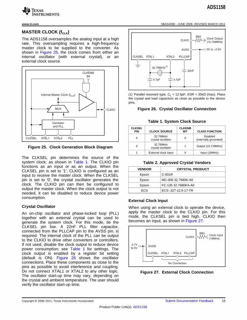
MASTER CLOCK (fCLK)
The ADS1158 oversamples the analog input at a highrate. This oversampling requires a high-frequencymaster clock to be supplied to the converter. Asshown in Figure 25, the clock comes from either aninternal oscillator (with external crystal), or anexternal clock source.
(1) Parallel resonant type. CL = 12.5pF, ESR = 35kΩ (max). Placethe crystal and load capacitors as close as possible to the devicepins.
Figure 26. Crystal Oscillator Connection
Table 1. System Clock Source
CLKSEL CLKENBPIN CLOCK SOURCE BIT CLKIO FUNCTION
32.768kHz Disabled0 0crystal oscillator (internally grounded)
32.768kHz0 1 Output (15.729MHz)Figure 25. Clock Generation Block Diagram crystal oscillator
1 External clock input X Input (16MHz)
The CLKSEL pin determines the source of thesystem clock, as shown in Table 1. The CLKIO pin Table 2. Approved Crystal Vendorsfunctions as an input or as an output. When the
VENDOR CRYSTAL PRODUCTCLKSEL pin is set to '1', CLKIO is configured as anEpson C-001Rinput to receive the master clock. When the CLKSELEpson MC-306 32.7680K-A0pin is set to '0', the crystal oscillator generates the
clock. The CLKIO pin can then be configured to Epson FC-135 32.7680KA-A0output the master clock. When the clock output is not ECS ECS-.327-12.5-17-TRneeded, it can be disabled to reduce device powerconsumption.
External Clock InputCrystal Oscillator When using an external clock to operate the device,
apply the master clock to the CLKIO pin. For thisAn on-chip oscillator and phase-locked loop (PLL)mode, the CLKSEL pin is tied high. CLKIO thentogether with an external crystal can be used tobecomes an input, as shown in Figure 27.generate the system clock. For this mode, tie the
CLKSEL pin low. A 22nF PLL filter capacitor,connected from the PLLCAP pin to the AVSS pin, isrequired. The internal clock of the PLL can be outputto the CLKIO to drive other converters or controllers.If not used, disable the clock output to reduce devicepower consumption; see Table 1 for settings. Theclock output is enabled by a register bit setting(default is ON). Figure 26 shows the oscillatorconnections. Place these components as close to thepins as possible to avoid interference and coupling.Do not connect XTAL1 or XTAL2 to any other logic. Figure 27. External Clock ConnectionThe oscillator start-up time may vary, depending onthe crystal and ambient temperature. The user shouldverify the oscillator start-up time.
Copyright © 2008–2011, Texas Instruments Incorporated Submit Documentation Feedback 15
Product Folder Link(s): ADS1158

128(4 + 4.26525 + TD) 2´11b DR CHOP-
fCLK
128[4 + CHOP(4.26525 + TD)] 2´11b DR CHOP-
fCLK
AnalogModulator
sinc5
Filter
ProgrammableAverager
Data Rate = f /128CLKModulator Rate = f /2CLK
Num_Ave
Data Rate /(128 ´= fCLK Num_Ave)(1)
ADS1158
SBAS429D –JUNE 2008–REVISED MARCH 2011 www.ti.com
Digital FilterMake sure to use a clock source clean from jitter orinterference. Ringing or under/overshoot should be The programmable low-pass digital filter receives theavoided. A 50Ω resistor in series with the CLKIO pin modulator output and produces a high-resolution(placed close to the source) can often help. digital output. By adjusting the amount of filtering,
tradeoffs can be made between resolution and dataADC rate—filter more for higher resolution, filter less for
higher data rate. The filter consists of two sections, aThe ADC block of the ADS1158 is composed of twofixed filter followed by a programmable filter.blocks: a modulator and a digital filter.Figure 28 shows the block diagram of the filter. Dataare supplied to the filter from the analog modulator atModulatora rate of fCLK/2. The fixed filter is a fifth-order sinc
The modulator converts the analog input voltage into filter with a decimation value of 64 that outputs dataa pulse code modulated (PCM) data stream. When at a rate of fCLK/128. The second stage of the filter isthe level of differential analog input (ADCINP – a programmable averager (first-order sinc filter) withADCINN) is near the level of the reference voltage, the number of averages set by the DRATE[1:0] bits.the '1' density of the PCM data stream is at its
The data rate depends upon the system clockhighest. When the level of the differential analog inputfrequency (fCLK) and the converter configuration. Theis near zero, the PCM '0' and '1' densities are nearlydata rate can be computed by Equation 1 orequal. The fourth-order modulator shifts theEquation 2:quantization noise to a high frequency (out of the
passband) where the digital filter can easily remove it. Data rate (Auto-Scan):The modulator continuously chops the input, resultingin excellent offset and offset drift performance. It is
(1)important to note that offset or offset drift thatoriginates from the external circuitry is not removed Data rate (Fixed-Channel mode):by the modulator chopping. These errors can beeffectively removed by using the external choppingfeature of the ADS1158 (see the External Chopping (2)section).
Where:DR = DRATE[1:0] register bits (binary).CHOP = Chop register bit.TD = time delay value given in Table 4 from theDLY[2:0] register bits (128/fCLK periods).
(1) Data rate for Fixed-Channel mode, Chop = 0, Delay = 0.
Figure 28. Block Diagram of Digital Filter
16 Submit Documentation Feedback Copyright © 2008–2011, Texas Instruments Incorporated
Product Folder Link(s): ADS1158

½H = H (f) H (f) =(f) sinc Averager½ ½ ½ ´ ½ ½5
5
sin128 f´p
fCLK
64 sin´2 fp ´fCLK
´
sin128 Num_Ave f´p ´
fCLK
Num_Ave sin´128 fp ´
fCLK
0
-20
-40
-60
-80
-100
-120
-140
Frequency (kHz)
Gain
(dB
)
125 2500 375 500 625
Data Rate
Auto-Scan Mode
(23.739kSPS)
Data Rate
Fixed-Channel Mode
(125kSPS)
0
-20
-40
-60
-80
-100
-120
-140
Frequency (kHz)
Gain
(dB
)
125 2500 375 500 625
Data Rate
Auto-Scan Mode
(15.123kSPS)
Data Rate
Fixed-Channel Mode
(31.25kSPS)
ADS1158
www.ti.com SBAS429D –JUNE 2008–REVISED MARCH 2011
Table 3 shows a listing of the averaging and data Figure 30 shows the response with averaging set to 4rates for each of the four DRATE[1:0] register (DRATE[1:0] = 10). 4-reading, post-averagingsettings for the Auto-Scan and Fixed-Channel modes, produces three equally-spaced notches betweenwith CHOP, DLY = 0. Note that the data rate scales each main notch of the sinc5 filter. The frequencydirectly with fCLK. For example, reducing fCLK by 2x response of DRATE[1:0] = 01 and 00 follows a similarreduces the maximum data rate by 2x. pattern, but with 15 and 63 equally-spaced notches
between the main sinc5 notches, respectively.FREQUENCY RESPONSE
The low-pass digital filter sets the overall frequencyresponse for the ADS1158. The filter response is theproduct of the responses of the fixed andprogrammable filter sections and is given byEquation 3:
(3)
The digital filter attenuates noise on the modulatorFigure 29. Frequency Response, DRATE[1:0] = 11output, including noise from within the ADS1158 and
external noise present within the ADS1158 inputsignal. Adjusting the filtering by changing the numberof averages used in the programmable filter changesthe filter bandwidth. With a higher number ofaverages, the bandwidth is reduced and more noiseis attenuated.
The low-pass filter has notches (or zeros) at the dataoutput rate and multiples thereof. The sinc5 part ofthe filter produces wide notches at fCLK/128 andmultiples thereof. At these frequencies, the filter haszero gain. Figure 29 shows the response with no postaveraging. Note that in Auto-Scan mode, the datarate is reduced while retaining the same frequencyresponse as in Fixed-Channel mode.
With programmable averaging, the wide notchesproduced by the sinc5 filter remain, but a number ofnarrow notches are superimposed in the response. Figure 30. Frequency Response, DRATE[1:0] = 10The number of the superimposed notches isdetermined by the number of readingsaveraged (minus one).
Table 3. Data Rates (1)
DATA RATE AUTO-SCAN DATA RATE FIXED-CHANNEL –3dB BANDWIDTHDRATE[1:0] Num_Ave (2) MODE (SPS) (3) MODE (SPS) (Hz)
11 1 23739 125000 25390
10 4 15123 31250 12402
01 16 6168 7813 3418
00 64 1831 1953 869
(1) fCLK = 16MHz, Chop = 0, and Delay = 0.(2) Num_Ave is the number of averages performed by the digital filter second stage.(3) In Auto-Scan mode, the data rate listed is for a single channel; the effective data rate for multiple channels (on a per-channel basis) is
the value shown in Figure 29 and Figure 30 divided by the number of active channels in a scan loop.
Copyright © 2008–2011, Texas Instruments Incorporated Submit Documentation Feedback 17
Product Folder Link(s): ADS1158

DRDY 1 2
Step Input
Data Not Settled Settled Data
DRDY 1 2 6
Step Input
Data Not Settled Settled Data
0
-20
-40
-60
-80
-100
-120
-140
Frequency (MHz)
Gain
(dB
)
4 80 12 16
DRATE[1:0] = 11
125kSPS
Fixed-Channel Mode
ADS1158
SBAS429D –JUNE 2008–REVISED MARCH 2011 www.ti.com
ALIASING applying asynchronous step inputs, the settling timeis somewhat different. The step-input settling time
The digital filter low-pass characteristic repeats at diagrams (Figure 32 and Figure 33) show themultiples of the modulator rate of fCLK/2. Figure 31 converter step response with an asynchronous stepshows the response plotted out to 16MHz at the data input. For most modes of operation, the analog inputrate of 125kSPS (Fixed-Channel mode). Notice how must be stable for one complete conversion cycle tothe responses near dc, 8MHz, and 16MHz are the provide settled data. In Fixed-Channel modesame. The digital filter attenuates high-frequency (DRATE[1:0] = 11), the input must be stable for fivenoise on the ADS1158 inputs up to the frequency complete conversion cycles.where the response repeats. However, noise orfrequency components present on the analog inputwhere the response repeats alias into the passband.For most applications, an anti-alias filter isrecommended to remove this noise. A simplefirst-order input filter with a pole at 200kHzprovides –34dB rejection at the first image frequency.
Figure 32. Asynchronous Step-Input SettlingTime (DRATE[1:0] = 10, 01, 00)
Figure 33. Asynchronous Step-Input SettlingTime (Fixed-Channel Mode, DRATE[1:0] = 11)
Figure 31. Frequency Response Out to 16MHz Table 4. Effective Data Rates with Switch-TimeDelay (Auto-Scan Mode) (1)
Referring to Figure 29 and Figure 30, frequenciesTIME
present on the analog input above the Nyquist rate DELAY TIME DRATE DRATE DRATE DRATEDLY (128/fCLK DELAY [1:0] = [1:0] = [1:0] = [1:0] =(sample rate/2) are first attenuated by the digital filter[2:0] periods) (μS) 11 10 01 00and then aliased into the passband.000 0 0 23739 15123 6168 1831
001 1 8 19950 13491 5878 1805SETTLING TIME010 2 16 17204 12177 5614 1779
The design of the ADS1158 provides fully-settled011 4 32 13491 10191 5151 1730
data when scanning through the input channels in100 8 64 9423 7685 4422 1639Auto-Scan mode. The DRDY flag asserts low when101 16 128 5878 5151 3447 1483the data for each channel are ready. It may be110 32 256 3354 3104 2392 1247necessary to use the automatic switch time delay111 48 384 2347 2222 1831 1075feature to provide time for settling of the external
buffer and associated components after channelswitching. When the converter is started (START pin (1) Time delay and data rates scale with fCLK. If Chop = 1, thetransitions high or Start Command) with stable inputs, data rates are half those shown. fCLK = 16MHz, Auto-Scanthe first converter output is fully settled. When mode.
18 Submit Documentation Feedback Copyright © 2008–2011, Texas Instruments Incorporated
Product Folder Link(s): ADS1158

ADS1158
www.ti.com SBAS429D –JUNE 2008–REVISED MARCH 2011
EXTERNAL MULTIPLEXER LOOP Use of the switch time delay register reduces theeffective channel data rate. Table 4 shows the actual
The external multiplexer loop consists of two data rates derived from Equation 1, when using thedifferential multiplexer output pins and two differential switch time delay feature.ADC input pins. The user may use externalcomponents (buffering/filtering, single-ended to When pulse converting, where one channel isdifferential conversion, etc.) to form a signal converted with each START pin pulse or each pulseconditioning loop. For best performance, the ADC command, the application software may provide theinput should be buffered and driven differentially. required time delay between pulses. However, with
Chop = 1, the switch time delay feature may continueTo bypass the external multiplexer loop, connect the to be necessary to allow for settling.ADC input pins directly to the multiplexer output pins,or select internal bypass connection (BYPASS = 0 of In estimating the time delay that may be required,CONFIG0). Note that the multiplexer output pins are Table 5 lists the time delay-to-time constant ratio (t/τ)active regardless of the bypass setting. and the corresponding final settled data in % and
number of bits.SWITCH TIME DELAY
Table 5. Settling TimeWhen using the ADS1158 in the Auto-Scan mode,
FINAL SETTLING FINAL SETTLINGwhere the converter automatically switches from onet/τ(1) (%) (Bits)channel to the next, the settling time of the external
1 63 2signal conditioning circuit becomes important. If thechannel does not fully settle after the multiplexer 3 95 5channel is switched, the data may not be correct. The 5 99.3 7ADS1158 provides a switch time delay feature which 7 99.9 10automatically provides a delay after channel switching
10 99.995 14to allow the channel to settle before taking a reading.15 99.998 16The amount of time delay required depends primarily
on the settling time of the external signal conditioning. (1) Multiple time constants can be approximated by:Additional consideration may be needed to account (τ1 2 + τ2 2+…).for the settling of the input source arising from thetransient generated from channel switching.
Copyright © 2008–2011, Texas Instruments Incorporated Submit Documentation Feedback 19
Product Folder Link(s): ADS1158

C
ISDC
=dt
dV
80W
AVDD
RL
RS
ADCINP
80W
AVSS
ADCINN
MUXOUTP
MUXOUTN
ISDC
ISDC
ADS1158
SBAS429D –JUNE 2008–REVISED MARCH 2011 www.ti.com
SENSOR BIAS The current source is connected to the output of themultiplexer. For unselected channels, the current
An integrated current source provides a means to source is not connected. This configuration meansbias an external sensor (for example, a diode that when a new channel is selected, the currentjunction); or, it verifies the integrity of a sensor or source charges stray sensor capacitance, which maysensor connection. When the sensor fails to an open slow the rise of the sensor voltage. The automaticcondition, the current sources drive the inputs of the switch time delay feature can be used to apply anconverter to positive full-scale. The biasing is in the appropriate time delay before a conversion is startedform of differential currents (programmable 1.5μA or to provide fully settled data (see the Switch Time24μA), connected to the output of the multiplexer. Delay section).Figure 34 shows a simplified diagram of ADS1158 The time to charge the external capacitance is giveninput structure with the external sensor modeled as a in Equation 4:resistance RS between two input pins. The two 80Ωseries resistors, RMUX, model the ADS1158 internalresistances. RL represents the effective input (4)resistance of the ADC input or external buffer. When
It is also important to note that the low impedancethe sensor bias is enabled, they source ISDC to one(65kΩ) of the direct ADC inputs or the impedance ofselected input pin (connected to the MUXOUTPthe external signal conditioning loads the currentchannel) and sink ISDC from the other selected inputsources. This low impedance limits the ability of thepin (connected to the MUXOUTN channel). Thecurrent source to pull the inputs to positive full-scalesignal measured with the biasing enabled equals thefor open-channel detection.total IR drop: ISDC[(2RMUX + RS) ׀׀ RL]. Note that when
the sensor is a direct short (that is, RS = 0), thereOPEN-SENSOR DETECTIONcontinues to be a small signal measured by the
ADS1158 when the biasing is enabled: ISDC[2RMUX ׀׀ For open-sensor detection, set the biasing to eitherRL]. 1.5μA or 24μA. Then select the channel and read the
output code. When a sensor opens, the positive inputis pulled to AVDD and the negative input is pulled toAVSS. Because of this configuration, the output codetrends toward positive full-scale. Note that theinteraction of the multiplexer resistance with thecurrent source may lead to degradation in converterlinearity. It is recommended to enable the currentsource only periodically to check for open inputs anddiscard the associated data.
EXTERNAL DIODE BIASING
The current source can be used to bias externaldiodes for temperature sensing. Scan the appropriatechannels with the current source set to 24µA.Re-scan the same channels with the current sourceset to 1.5µA. The difference in diode voltage readingsresulting from the two bias currents is directlyproportional to temperature.
Note that errors in current ratio, diode and cableFigure 34. Sensor Bias Structureresistance, or the non-ideality factor of the diode canlead to errors in temperature readings. These effectscan be compensated by characterization or bycalibrating the diode at known temperatures.
20 Submit Documentation Feedback Copyright © 2008–2011, Texas Instruments Incorporated
Product Folder Link(s): ADS1158
ADC
Multiplexer
(chopping)
AINn
AINn
MUXOUTP
MUXOUTN
ADCINP
Optional
Signal
Conditioning
ADCINN
GPIO Pin
GPIO Data (read)
GPIO Data (write)
GPIO Control
ADS1158
www.ti.com SBAS429D –JUNE 2008–REVISED MARCH 2011
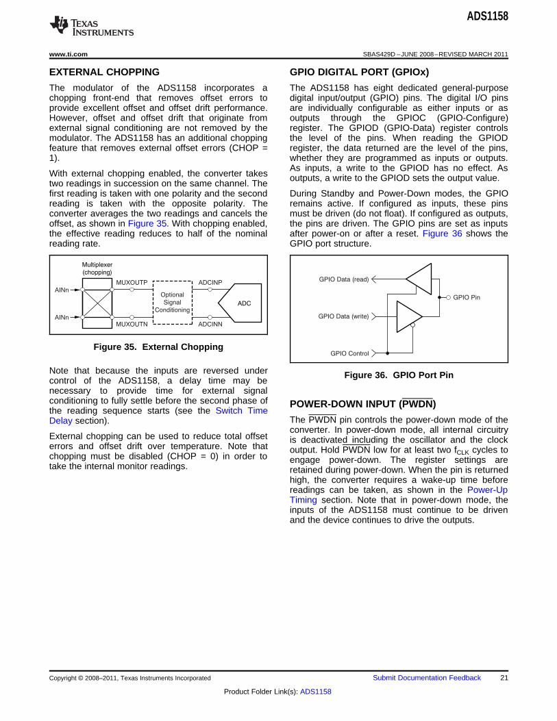
EXTERNAL CHOPPING GPIO DIGITAL PORT (GPIOx)
The modulator of the ADS1158 incorporates a The ADS1158 has eight dedicated general-purposechopping front-end that removes offset errors to digital input/output (GPIO) pins. The digital I/O pinsprovide excellent offset and offset drift performance. are individually configurable as either inputs or asHowever, offset and offset drift that originate from outputs through the GPIOC (GPIO-Configure)external signal conditioning are not removed by the register. The GPIOD (GPIO-Data) register controlsmodulator. The ADS1158 has an additional chopping the level of the pins. When reading the GPIODfeature that removes external offset errors (CHOP = register, the data returned are the level of the pins,1). whether they are programmed as inputs or outputs.
As inputs, a write to the GPIOD has no effect. AsWith external chopping enabled, the converter takes outputs, a write to the GPIOD sets the output value.two readings in succession on the same channel. Thefirst reading is taken with one polarity and the second During Standby and Power-Down modes, the GPIOreading is taken with the opposite polarity. The remains active. If configured as inputs, these pinsconverter averages the two readings and cancels the must be driven (do not float). If configured as outputs,offset, as shown in Figure 35. With chopping enabled, the pins are driven. The GPIO pins are set as inputsthe effective reading reduces to half of the nominal after power-on or after a reset. Figure 36 shows thereading rate. GPIO port structure.
Figure 35. External Chopping
Note that because the inputs are reversed under Figure 36. GPIO Port Pincontrol of the ADS1158, a delay time may benecessary to provide time for external signalconditioning to fully settle before the second phase of POWER-DOWN INPUT (PWDN)the reading sequence starts (see the Switch Time
The PWDN pin controls the power-down mode of theDelay section).converter. In power-down mode, all internal circuitry
External chopping can be used to reduce total offset is deactivated including the oscillator and the clockerrors and offset drift over temperature. Note that output. Hold PWDN low for at least two fCLK cycles tochopping must be disabled (CHOP = 0) in order to engage power-down. The register settings aretake the internal monitor readings. retained during power-down. When the pin is returned
high, the converter requires a wake-up time beforereadings can be taken, as shown in the Power-UpTiming section. Note that in power-down mode, theinputs of the ADS1158 must continue to be drivenand the device continues to drive the outputs.
Copyright © 2008–2011, Texas Instruments Incorporated Submit Documentation Feedback 21
Product Folder Link(s): ADS1158

CLKIO
Device Ready
tWAKE
3.2V, typical
CLKSEL
or
AVDD AVSS-
(1)
or
PWDN
CLKIO
Device Ready
tWAKE
3.2V, typical
or
AVDD AVSS-
(1)
PWDN,
CLKSEL
ADS1158
SBAS429D –JUNE 2008–REVISED MARCH 2011 www.ti.com
Table 6. Wake-Up TimesPOWER-UP TIMINGtWAKEWhen powering up the device or taking the PWDN
INTERNAL tWAKEpin high to wake the device, a wake-up time is CONDITION OSCILLATOR(1) EXTERNAL CLOCKrequired before readings can be taken. When using
PWDN or CLKSEL tOSC 2/fCLKthe internal oscillator, the wake-up time is composedAVDD – AVSS tOSC + 218/fCLK 218/fCLKof the oscillator start-up time and the PLL lock time,
and if the supplies are also being powered, there is a (1) Wake-up times for the internal oscillator operation are typicalreset interval time of 218 fCLK cycles. Note that CLKIO and may vary depending on crystal characteristics and layout
capacitance. The user should verify the oscillator start-upis not valid during the wake-up period, as shown intimes (tOSC = oscillator start-up time).Figure 37.
POWER-UP SEQUENCE
The analog and digital supplies should be appliedbefore any analog or digital input is driven. The powersupplies may be sequenced in any order. The internalmaster reset signal is generated from the analogpower supply (AVDD – AVSS), when the levelreaches approximately 3.2V. The power-up masterreset signal is functionally the same as the ResetCommand and the RESET input pin.
Reset Input (RESET)
When RESET is held low for at least two fCLK cycles,all registers are reset to their default values and the
(1) Shown with DVDD stable. digital filter is cleared. When RESET is released high,the device is ready to convert data.Figure 37. Device Wake Time with
Internal OscillatorClock Select Input (CLKSEL)
This pin selects the source of the system clock: theWhen using the device with an external clock, thecrystal oscillator or an external clock. Tie CLKSELwake-up time is 2/fCLK periods when waking up withlow to select the crystal oscillator. When using anthe PWDN pin and 218/fCLK periods when poweringexternal clock (applied to the CLKIO pin), tie CLKSELthe supplies, all after a valid CLKIO is applied, ashigh.shown in Figure 38.
Clock Input/Output (CLKIO)
This pin serves either as a clock output or clock input,depending on the state of the CLKSEL pin. Whenusing an external clock, apply the clock to this pinand set the CLKSEL pin high. When using theinternal oscillator, this pin has the option of providinga clock output. The CLKENB bit of register CONFIG0enables the clock output (default is enabled).
Start Input (START)
The START pin is an input that controls the ADC(1) Shown with DVDD stable.process. When the START pin is taken high, the
Figure 38. Device Wake Time with External Clock converter starts converting the selected inputchannels. When the START pin is taken low, theconversion in progress runs to completion and theTable 6 summarizes the wake-up times using theconverter is stopped. The device then enters one ofinternal oscillator and the external clock operations.the two idle modes (see the Idle Modes section formore details). See the Conversion Control section fordetails of using the START pin.
22 Submit Documentation Feedback Copyright © 2008–2011, Texas Instruments Incorporated
Product Folder Link(s): ADS1158

DRDY
DRDY
SCLK
SCLK
DRDY with SCLK
DRDY without SCLK
tDRDYPLS
t =DRDYPLS
1
fCLK
ADS1158
www.ti.com SBAS429D –JUNE 2008–REVISED MARCH 2011
Data Ready Output (DRDY) DRDY is usually connected to an interrupt of acontroller, DSP, or connected to a controller port pinThe DRDY pin is an output that asserts low tofor polling in a software loop. Channel data can beindicate when new channel data are available to readread without the use of DRDY. Read the data using(the previous conversion data are lost). DRDY returnsthe register format read and check the Status Bytehigh after the first falling edge of SCLK during a datawhen the NEW bit = 1, which indicates new channelread operation. If the data are not read (no SCLKdata.pulses), DRDY remains low until new channel data
are available once again. DRDY then pulses high,Output Data Scaling and Over-Rangethen low to indicate new data are available; see
Figure 39. The ADS1158 is scaled such that the output datacode resulting from an input voltage equal to ±VREFhas a margin of 6.6% before clipping. Thisarchitecture allows operation of applied input signalsat or near full-scale without overloading the converter.
Specifically, the device is calibrated so that:
1LSB = VREF/7800h,
and the output clips when:
|VIN| ≥ 1.06 × VREF.
Table 7 summarizes the ideal output codes versusinput signals.
Figure 39. DRDY Timing(See Figure 2 for the DRDY Pulse)
Table 7. Ideal Output Code versus Input Signal
INPUT SIGNAL VIN(ADCINP – ADCINN) IDEAL OUTPUT CODE (1) DESCRIPTION
≥ +1.06 VREF 7FFFh Maximum positive full-scale before output clipping
+VREF 7800h VIN = +VREF
+1.06 VREF/(215 – 1) 0001h +1LSB
0 0000h Bipolar Zero
–1.06 VREF/(215 – 1) FFFFh –1LSB
–VREF 87FFh VIN = –VREF
≤ –1.06 VREF × (215/215 – 1) 8000h Maximum negative full-scale before output clipping
(1) Ideal output code –0.5LSB excludes effects of noise, linearity, offset, and gain errors.
Copyright © 2008–2011, Texas Instruments Incorporated Submit Documentation Feedback 23
Product Folder Link(s): ADS1158

3072 (C0 h)0
CodeExternal Reference (V) =
3072 (C0 h)0
CodeTotal Analog Supply Voltage (V) =
30720 (7800h)
CodeDevice Gain (V/V) =
Temp Sensor Coefficient
Temp Reading( V) 168,000 V-m mTemperature ( C) =° + 25°C
ADS1158
SBAS429D –JUNE 2008–REVISED MARCH 2011 www.ti.com
Reference Reading (REF)INTERNAL SYSTEM READINGSIn this configuration, the external reference is
Analog Power-Supply Reading (VCC) connected to the analog input and an internalreference is connected to the reference of the ADC.The analog power-supply voltage of the ADS1158The data from this register indicate the magnitude ofcan be monitored by reading the VCC register. Thethe external reference voltage.supply voltage is routed internal to the ADS1158 and
is measured and scaled using an internal reference. The scale factor of Equation 7 converts the codeThe supply readback channel outputs the difference value to external reference voltage:between AVDD and AVSS (AVDD – AVSS), for bothsingle and dual configurations. Note that it is requiredto disable chopping (CHOP = 0) before taking this (7)reading.
This readback function can be used to check forThe scale factor of Equation 5 converts the code missing or an out-of-range reference. If the referencevalue to volts: input pins are floating (not connected), internal
biasing pulls them to the AVSS supply. This pullcauses the output code to tend toward '0'. Bypass
(5) capacitors connected to the external reference pinsmay slow the response of the pins when open. WhenWhen the power supply falls below the minimumreading this register immediately after power-on,specified operating voltage, the full operation of theverify that the reference has settled to ensure anADS1158 cannot be ensured. Note that when theaccurate reading. Note that it is required to disabletotal analog supply voltage falls to belowchopping (CHOP = 0) before taking this reading.approximately 4.3V, the returned data are set to zero.
The SUPPLY bit in the status byte is then set. The bitTemperature Reading (TEMP)clears when the total supply voltage rises
approximately 50mV higher than the lower trip point. The ADS1158 contains an on-chip temperaturesensor. This sensor uses two internal diodes with oneThe digital supply (DVDD) may be monitored bydiode having a current density of 16x of the other.looping-back the supply voltage to an input channel.The difference in current densities of the diodesA resistor divider may be required for bipolar supplyyields a difference voltage that is proportional tooperation to reduce the DVDD level to within theabsolute temperature.range of the analog supply.
As a result of the low thermal resistance of theGain Reading (GAIN) package to the printed circuit board (PCB), the
internal device temperature tracks the PCBIn this configuration, the external reference istemperature closely. Note also that self-heating of theconnected both to the analog input and to theADS1158 causes a higher reading than thereference input of the ADC. The data from thistemperature of the surrounding PCB. Note that it isregister indicate the gain of the device.required to disable chopping (CHOP = 0) before
The following scale factor (Equation 6) converts the taking this reading.code value to device gain:
The scale factor of Equation 8 converts thetemperature reading to °C. Before using the equation,
(6) the temperature reading code must first be scaled tomicrovolts.To correct the device gain error, the user software
can divide each converter data value by the devicegain. Note that this corrects only for gain errorsoriginating within the ADC; system gain errors that
(8)occur because of an external gain stage error orbecause of reference errors are not compensated. Where Temp Sensor Coeff = 563μV/°C (if theNote that it is also required to disable chopping ADS1158 and test PCB temperatures are forced(CHOP = 0) before taking this reading. together), or 394μV/°C if only the ADS1158
temperature is forced and the test PCB is in freeair.
24 Submit Documentation Feedback Copyright © 2008–2011, Texas Instruments Incorporated
Product Folder Link(s): ADS1158

DRDY
START Pin
Data Ready, Index to Next Channel
IdleIdle Mode Converting
DRDY
START Pin
Pulse Convert
Command
Converting ConvertingIdle
Data Ready, Index to Next Channel
or
DRDY
START Pin
tSDSU
tDRHD
SYMBOL DESCRIPTION MIN UNIT
tSDSU 8 tCLK
8 tCLKtDRHD
START to Setup TimeDRDY
to Halt Further Conversions
DRDY to START Hold Time
to Complete Current Conversion
ADS1158
www.ti.com SBAS429D –JUNE 2008–REVISED MARCH 2011
Offset Reading (OFFSET)
The differential output of the multiplexer is shortedtogether and set to a common-mode voltage of(AVDD – AVSS)/2. Ideally, the code from this registerfunction is 0h, but varies because of the noise of theADC and offsets stemming from the ADC andexternal signal conditioning. This register can be usedto calibrate or track the offset of the ADS1158 and Figure 40. Conversion Control, Auto-Scan Modeexternal signal conditioning. The chop feature of theADC can automatically remove offset and offset drift
Pulse Convert Commandfrom the external signal conditioning; see the ExternalChopping section. Figure 41 also shows the start of conversions with the
rising edge of the START pin. If the START pin isCONVERSION CONTROL taken high, and then low before completion of the
conversion cycle (8 τCLK before DRDY asserts low),The conversions of the ADS1158 are controlled byonly the current channel is converted and the devicethe START pin. Conversions begin when the STARTenters the standby or sleep modes and waits for apin is taken high and conversions are stopped whennew start condition. Figure 42 shows the START pinthe START pin is taken low. For continuousto DRDY timing. The same function of conversionconversions, tie the START pin high. The START pincontrol is possible using the Pulse Convert commandcan also be tied low and the conversions controlled(with the START pin low). In this operation, the databy the PULSE convert command. The PULSEfrom one channel are converted with each Pulseconvert command converts one channel (only) forConvert command. The Pulse convert commandeach command sent. In this way, channeltakes effect when the command byte is completelyconversions can be stepped without the need toshifted in (eighth falling edge of SCLK). Aftertoggle the START pin.conversion, if more than one channel is enabled(Auto-Scan mode), the converter indexes to the nextSTART Pinselected channel after completing the conversion.
As shown in Figure 40, when the START pin is takenhigh, conversions start beginning with the currentchannel. The device continues to convert all of theprogrammed channels, in a continuous loop, until theSTART pin is taken low. When this occurs, theconversion in process completes, and the deviceenters the standby or sleep mode and waits for a newstart condition. When DRDY asserts low, theconversion data are ready. Figure 42 shows theSTART pin to DRDY timing. The order in whichchannel data are converted is described in Table 9.When the last selected channel in the program listhas been converted, the device continues Figure 41. Pulse Conversion, Auto-Scan Modeconversions starting with the highest priority channel.If there is only one channel selected in the Auto-Scanmode, the converter remains fixed on one channel. Awrite operation to any of the multiplexer channelselect registers sets the channel pointer to thehighest priority channel (see Table 10). InFixed-Channel mode, the channel pointer remainsfixed.
Figure 42. START Pin and DRDY Timing
Copyright © 2008–2011, Texas Instruments Incorporated Submit Documentation Feedback 25
Product Folder Link(s): ADS1158

Initial Delay
Fully-Settled Data
DRDY
Start
Condition
ADS1158
SBAS429D –JUNE 2008–REVISED MARCH 2011 www.ti.com
GPIO Linked START Pin Control Power-Down mode. In Converting mode, the deviceis actively converting channel data. The device powerThe START pin can be controlled directly by softwaredissipation is the highest in this mode. This mode isby connecting externally a GPIO port pin to thedivided into two sub-modes: Auto-Scan andSTART pin. (Note that an external pull-down resistorFixed-Channel.is recommended to keep the GPIO from floating until
the GPIO is configured as an output). For this mode The next mode is the Idle mode. In this mode, theof control, the START pin is effectively controlled by device is not converting channel data. The devicewriting to the GPIO Data Register (GPIOD), with the remains active, waiting for input to start conversions.write operation setting or resetting the appropriate bit. The power consumption is reduced from that of theThe data takes effect on the eighth falling edge of the Converting mode. This mode also has twodata byte write. The START pin can then be sub-modes: Standby and Sleep.controlled by the serial interface.
The last mode is Power-Down mode. In this mode, allfunctions of the converter are disabled to reduceInitial Delaypower consumption to a minimum.
As seen in Figure 43, when a start convert conditionoccurs, the first reading from ADS1158 is delayed for CONVERTING MODESa number of clock cycles. This delay allows fully
The ADS1158 has two converting modes: Auto-Scansettled data to occur at the first data read. Data readsand Fixed-Channel. In Auto-Scan mode, the channelsthereafter are available at the full data rate. Theto be measured are pre-selected in the addressnumber of clock cycles delayed before the firstregister settings. When a convert condition is present,reading is valid depends on the data rate setting, andthe converter automatically measures and sequenceswhether exiting the Standby or Sleep mode. Table 8through the channels either in a continuous loop orlists the delayed clock cycles versus data rate.pulse-step fashion, depending on the triggercondition.
In Fixed-Channel mode, the channel address isselected in the address register settings beforeacquiring channel data. When a convert condition ispresent, the device converts a single channel, eithercontinuously or in pulse-step fashion, depending onthe trigger condition. The data rate in this mode ishigher than in Auto-Scan mode because the inputchannels are not indexed for each reading.
Figure 43. Start Condition to First Data The selection of converting modes is set with bitMUXMOD of register CONFIG0.
OPERATING MODES
The operating modes of the ADS1158 are defined inthree basic states: Converting mode, Idle mode, and
Table 8. Start Condition to DRDY Delay, Chop = 0, DLY[2:0] = 000
INITIAL DELAY (Standby Mode) INITIAL DELAY (Sleep Mode)(fCLK cycles) (fCLK cycles)
DRATE[1:0] Fixed-Channel Auto-Scan Fixed-Channel Auto-Scan
11 802 708 866 772
10 1186 1092 1250 1156
01 2722 2628 2786 2692
00 8866 8772 8930 8836
26 Submit Documentation Feedback Copyright © 2008–2011, Texas Instruments Incorporated
Product Folder Link(s): ADS1158
ADS1158
www.ti.com SBAS429D –JUNE 2008–REVISED MARCH 2011
Auto-Scan Mode Fixed-Channel Mode
The ADS1158 provides 16 analog inputs that can be In this mode, any of the 16 analog input channelsconfigured in combinations of eight differential inputs (AIN0–AIN15) can be selected for the positive ADCor 16 single-ended inputs. The device also provides input and any analog input channels can be selectedan additional five internal system measurements. for the negative ADC input. New channelTaken together, the device allows a total of 29 configurations must be selected by the MUXSCHpossible channel measurements. The converter
register before converting a different channel. Noteautomatically scans and measures the selectedthat the AINCOM input and the internal systemchannels, either in a continuous loop or pulse-stepregisters cannot be referenced in this mode.fashion, under the control of the START pin or Start
command software. The channels are selected forIdle Modesmeasurement in registers MUXDIF, MUXSG0,
MUXSG1, and SYSRED. When any of these registers When the START pin is taken low, the deviceare written, the internal channel pointer is set to the completes the conversion of the current channel andchannel address with the highest priority (see then enters one of the Idle modes, Standby or Sleep.Table 10). In the Standby mode, the internal biasing of the
converter is reduced. This state provides the fastestDRDY asserts low when the channel data are ready;wake-up response when re-entering the run state. Insee Figure 41 and Figure 40. At the same time, theSleep mode, the internal biasing is reduced further toconverter indexes to the next selected channel and, ifprovide lower power consumption than the Standbythe START pin is high, starts a new channelmode. This mode has a slower wake-up responseconversion. Otherwise, if pulse converting, the devicewhen re-entering the Converting mode (see Table 8).enters the Idle mode.Selection of these modes is set under bit IDLMOD of
For example, if channels 3, 4, 7, and 8 are selected register CONFIG1.for measurement in the list, the ADS1158 convertsthe channels in that order, skipping all other POWER-DOWN MODEchannels. After channel 8 is converted, the device
In power-down mode, both the analog and digitalstarts over, beginning at the top of the channel list,circuitry are completely disabled.channel 3.
The following guidelines can be used when selecting SERIAL INTERFACEinput channels for Auto-Scan measurement:
The ADS1158 is operated via an SPI-compatible1. For differential measurements, adjacent input serial interface by writing data to the configuration
pins (AIN0/AIN1, AIN2/AIN3, AIN4/AIN5, etc.) are registers, using commands to control the converterpre-set as differential pairs. Even number and finally reading back the channel data. Thechannels from each pair represent the positive interface consists of four signals: CS, SCLK, DIN,input to the ADC and odd number channels within and DOUT.a pair represent the negative input (for example,AIN0/AIN1: AIN0 is the positive channel, AIN1 is Chip Select (CS)the negative channel.)
CS is an input that selects the device for serial2. For single-ended measurements, use AIN0communication. CS is active low. When CS is high,through AIN15 as single-ended inputs; AINCOMread or write commands in progress are aborted andis the shared common input among them. Note:the serial interface is reset. Additionally, DOUT goesAINCOM does not need to be at ground potential.to a 3-state condition and inputs on DIN are ignored.For example, AINCOM can be tied to VREFP orDRDY indicates when data are ready, independent ofVREFN; or any potential between (AVSS –CS.100mV) and (AVDD + 100mV).
3. Combinations of differential, single-ended inputs, The converter may be operated using CS to activelyand internal system registers can be used in a select and deselect the device, or with CS tied lowscan. (always selected). CS must stay low for the entire
read or write operation. When operating with CS tiedlow, the number of SCLK pulses must be carefullycontrolled to avoid false command transmission.
Copyright © 2008–2011, Texas Instruments Incorporated Submit Documentation Feedback 27
Product Folder Link(s): ADS1158

ADS1158
SBAS429D –JUNE 2008–REVISED MARCH 2011 www.ti.com
Serial Clock (SCLK) Operation Reading DATA
The serial clock (SCLK) is an input that is used to DRDY goes low to indicate that new conversion dataclock data into (DIN) and out of (DOUT) the are ready. The data may be read via a direct dataADS1158. This input is a Schmitt-trigger input that read (Channel Data Read Direct) or in a registerhas a high degree of noise immunity. However, it is format (Channel Data Read Register). A direct datarecommended to keep SCLK as clean as possible to read requires the data to be read before the nextprevent glitches from inadvertently shifting the data. occurrence of DRDY or the data are corrupted. ThisData are shifted into DIN on the rising edge of SCLK type of data read requires synchronization with DRDYand data are shifted out of DOUT on the falling edge to avoid this conflict. When reading data in theof SCLK. If SCLK is held inactive for 4096 or 256 fCLK register format, the data may be read at any timecycles (SPIRST bit of register CONFIG0), read or without concern to DRDY. The NEW bit of thewrite operations in progress terminate and the SPI STATUS byte indicates that the data register hasinterface resets. This timeout feature can be used to been refreshed with new converter data since the lastrecover lost communication when a serial interface read operation. The data are shifted out MSB firsttransmission is interrupted or inadvertently glitched. after the STATUS byte.
It should be noted that on system power-up, if theData Input (DIN) and Data Output (DOUT)ADS1158 interface signals are floating or undefined,Operationthe interface could wake in an unknown state. This
The data input pin (DIN) is used to input data to the condition is remedied by resetting the interface inADS1158. The data output pin (DOUT) is used to three ways: toggle the RESET pin low then high;output data from the ADS1158. Data on DIN is shifted toggle the CS pin high then low; or hold SCLKinto the converter on the rising edge of SCLK while inactive for 218 + 4096 fCLK cycles.data are shifted out on DOUT on the falling edge ofSCLK. DOUT 3-states when CS is high to allow Channel Data Read Directmultiple devices to share the line.
Channel data can be accessed from the ADS1158 intwo ways: Direct data read or data read with registerSPI Bus Sharingformat. With Direct read, the DIN input pin is held
The ADS1158 can be connected to a shared SPI bus. inactive (high or low) for at least the first three SCLKDOUT 3-states when CS is deselected (high). When transitions. When the first three bits are 000 or 111,the ADS1158 is connected to a shared bus, data can the device detects a direct data read and channelbe read only by the Channel Data Read command data are output. After the device detects this readformat. format, commands are ignored until either CS is
toggled, an SPI timeout occurs or the device is reset.COMMUNICATION PROTOCOL The Channel Data Read command does not have
this requirement.Communicating with the ADS1158 involves shiftingdata into the device (via the DIN pin) or shifting dataout of the device (via the DOUT pin) under control ofthe SCLK input.
28 Submit Documentation Feedback Copyright © 2008–2011, Texas Instruments Incorporated
Product Folder Link(s): ADS1158

1 2 3 4 5 6 7 8 1 2 3 4 5 6 7 8 1 2 3 4 5 6 7 8(1)
DRDY
CS
SCLK
DOUT
DIN
(hold inactive)
Status Byte(2) Data Byte 1 (MSB) Data Byte 2 (LSB)
(3)
CS
SCLK
DIN Command Byte 1 Don't Care Don't Care(1)
DOUT Don't Care Data(2)
Data(2)
1 2 3 4 5 6 7 8 1 2 3 4 5 6 7 8 1 2 3 4 5 6 7 8
ADS1158
www.ti.com SBAS429D –JUNE 2008–REVISED MARCH 2011
Channel Data Read CommandConcurrent with the first SCLK transition, channeldata are output on the DOUT output pin. A total of 16 To read channel data in this mode (register format),or 24 SCLK transitions complete the data read the first three bits of the command byte to be shiftedoperation. The number of shifts depend on whether into the device are 001. The MUL bit must be setthe status byte is enabled. The data must be because this command is a multiple byte read. Thecompletely shifted out before the next occurrence of remaining bits are don’t care but must be clocked toDRDY or the remaining data are corrupted. It is the device. During this time, ignore any data thatrecommended to monitor DRDY to synchronize the appear on DOUT until the command completes.start of the read operation to avoid data corruption. These data should be ignored. Beginning with theBefore DRDY asserts low, the MSB of the Status byte eighth SCLK falling edge (command byte completed),or the MSB of the data are output on DOUT (CS = the MSB of the channel data are restarted on DOUT.'0'), as shown in Figure 44. In this format, reading the The user clocks the data on the following rising edgedata a second time within the same DRDY frame of SCLK. A total of 32 SCLK transitions complete thereturns data = 0. data read operation. Unlike the direct read mode, the
channel data can be read during a DRDY transitionCOMMAND DESCRIPTION without data corruption. This mode is recommended
when DRDY is not used and the data are polled toCommands may be sent to the ADS1158 with CS tieddetect for the occurrence of new data or when CS islow. However, after the Channel Data Read Directtied low to avoid the necessity for an SPI timeout thatoperation, it is necessary to toggle CS or an SPIotherwise occurs when reading data directly. Thistimeout must occur to reset the interface beforeoption avoids conflicts with DRDY, as shown insending a command.Figure 45.
(1) No SCLK activity.
(2) Optional for Auto-Scan mode, disabled for Fixed-Channel mode. See Table 12, Status Byte.
(3) After the channel data read operation, CS must be toggled or an SPI timeout must occur before sending commands.
Figure 44. Channel Data Read Direct (No Command)
(1) After the prescribed number of registers are read, then one or more additional commands can be issued in succession.
(2) Three bytes for channel data register read. See Table 12, Status Byte. One or more bytes for register read, depending on MUL bit.
Figure 45. Register and Channel Data (Register Format) Read
Copyright © 2008–2011, Texas Instruments Incorporated Submit Documentation Feedback 29
Product Folder Link(s): ADS1158

1 2 3 4 5 6 7 8 1 2 3 4 5 6 7 8 1 2 3 4 5 6 7 8
CS
SCLK
DIN Command Byte Register Data(1)
Register Data(1)(2)
1 2 3 4 5 6 7 8 1 2 3 4 5 6 7 8 1 2 3 4 5 6 7 8
CS
SCLK
DIN Command 1 Command 2(1)
Command 3(1)
ADS1158
SBAS429D –JUNE 2008–REVISED MARCH 2011 www.ti.com
Register Read Command Beginning with the eighth SCLK rising edge(command byte completed), the MSB of the data areTo read register data, the first three bits of theshifted in. The remaining seven SCLK rising edgescommand byte to be shifted into the device are 010.complete the write to a single register. If MUL = '1',These bits are followed by the multiple register readthe data to the next register can be written bybit (MUL). If MUL = '1', then multiple registers can besupplying additional SCLKs. The operation terminatesread in sequence beyond the desired register. Ifwhen the last register is accessed (address = 09h),MUL = '0', only data from the addressed register canas shown in Figure 46.be read. The last four bits of the command word are
the beginning register address bits. During this time,CONTROL COMMANDSthe invalid data may appear on DOUT until the
command is completed. These data should bePulse Convert Commandignored. Beginning with the eighth falling edge of
SCLK (command byte completed), the MSB of the See Conversion Control section.register data are output on DOUT. The remainingeight SCLK transitions complete the read of a single Reset Commandregister. If MUL = '1', the data from the next register
The Reset command resets the ADC. All registerscan be read in sequence by supplying additionalare reset to their default values. A conversion inSCLKs. The operation terminates when the lastprocess continues but will be invalid when completedregister is accessed (address = 09h); see Figure 45.(DRDY low). This conversion data should bediscarded. Note that the SPI interface may requireRegister Write Commandreset for this command, or any command, to function.
To write register data, the first three bits of the To ensure device reset under a possible locked SPIcommand byte to be shifted into the device are 011. interface condition, do one of the following: 1) toggleThese bits are followed by the multiple register read CS high then low and send the reset command; or 2)bit (MUL). If MUL = '1', then multiple registers can be hold SCLK inactive for 256/fCLK or 4096/fCLK and sendwritten in sequence beyond the desired register. If the reset command. The control commands areMUL = '0', only data to the addressed register can be illustrated in Figure 47.written. The remaining four bits of the command wordare the beginning register address bits. During thistime, the invalid data may appear on DOUT until thecommand is completed. These data should beignored.
(1) One or more bytes, depending on MUL bit.
(2) After the prescribed number of registers are read, then one or more additional commands can be issued in succession.
Figure 46. Register Write Operation
(1) One or more additional commands can be issued in succession.
Figure 47. Control Command Operation
30 Submit Documentation Feedback Copyright © 2008–2011, Texas Instruments Incorporated
Product Folder Link(s): ADS1158

DRDY
NEW Bit
Data Reads
(register format)
ADS1158
www.ti.com SBAS429D –JUNE 2008–REVISED MARCH 2011
CHANNEL DATA
The data read operation outputs either three bytes (one byte for status and two bytes for data), or two bytes fordata only. The selection of the 3-byte or 2-byte data read is set by the bit STAT in register CONFIG0 (seeTable 12, Status Byte, for options). In the 3-byte read, the first byte is the status byte and the following two bytesare the data bytes. The MSB (Data15) of the data are shifted out first.
Table 9. CHANNEL DATA FORMAT
BYTE BIT 7 BIT 6 BIT 5 BIT 4 BIT 3 BIT 2 BIT 1 BIT 0
1 STATUS NEW OVF SUPPLY CHID4 CHID3 CHID2 CHID1 CHID0
2 MSB Data15 Data14 Data13 Data12 Data11 Data10 Data9 Data8
3 LSB Data7 Data6 Data5 Data4 Data3 Data2 Data1 Data0
STATUS BYTE
BIT STATUS.7, NEW
The NEW bit is set when the results of a Channel Data Read Command returns new channel data. The bitremains set indefinitely until the channel data are read. When the channel data are read again before theconverter updates with new data, the previous data are output and the NEW bit is cleared. If the channel dataare not read before the next conversion update, the data from the previous conversion is lost. As shown inFigure 48, the NEW bit emulates the operation of the DRDY output pin. To emulate the function of the DRDYoutput pin in software, the user reads data at a rate faster than the converter data rate. The user then polls theNEW bit to detect for new channel data.
0 = Channel data have not been updated since the last read operation.
1 = Channel data have been updated since the last read operation.
Figure 48. NEW Bit Operation
BIT STATUS.6, OVF
When this bit is set, it indicates that the differential voltage applied to the ADC inputs have exceeded the rangeof the converter |VIN| > 1.06VREF. During over-range, the output code of the converter clips to either positive FS(VIN ≥ 1.06 × VREF) or negative FS (VIN ≤ –1.06 × VREF). This bit, with the MSB of the data, can be used todetect positive or negative over-range conditions. Note that because of averaging incorporated within the digitalfilter, the absence of this bit does not assure that the modulator of the ADC has not saturated as a result ofpossible transient input overload conditions.
BIT STATUS.5, SUPPLY
This bit indicates that the analog power-supply voltage (AVDD – AVSS) is below a preset limit. The SUPPLY bitis set when the value falls below 4.3V (typically) and is reset when the value rises 50mV higher (typically) thanthe lower trip point. The output data of the ADC may not be valid under low power-supply conditions.
BITS CHID[4:0] CHANNEL ID BITS
The Channel ID bits indicate the measurement channel of the acquired data. Note that for Fixed-Channel mode,the Channel ID bits are undefined. See Table 10 for the channel ID, the measurement priority, and the channeldescription for Auto-Scan Mode.
Copyright © 2008–2011, Texas Instruments Incorporated Submit Documentation Feedback 31
Product Folder Link(s): ADS1158

ADS1158
SBAS429D –JUNE 2008–REVISED MARCH 2011 www.ti.com
BITS DATA[15:0] OF DATA BYTES
The ADC output data are 16 bits wide (DATA[15:0]). DATA15 is the most significant bit (MSB) and DATA0 is theleast significant bit (LSB). The data are coded in binary twos complement (BTC) format.
Table 10. Channel ID and Measurement Order (Auto-Scan Mode)
BITS CHID[4:0] PRIORITY CHANNEL DESCRIPTION
00h 1 (highest) DIFF0 (AIN0–AIN1) Differential 0
01h 2 DIFF1 (AIN2–AIN3) Differential 1
02h 3 DIFF2 (AIN4–AIN5) Differential 2
03h 4 DIFF3 (AIN6–AIN7) Differential 3
04h 5 DIFF4 (AIN8– AIN9) Differential 4
05h 6 DIFF5 (AIN10–AIN11) Differential 5
06h 7 DIFF6 (AIN12–AIN13) Differential 6
07h 8 DIFF7 (AIN14–AIN15) Differential 7
08h 9 AIN0 Single-ended 0
09h 10 AIN1 Single-ended 1
0Ah 11 AIN2 Single-ended 2
0Bh 12 AIN3 Single-ended 3
0Ch 13 AIN4 Single-ended 4
0Dh 14 AIN5 Single-ended 5
0Eh 15 AIN6 Single-ended 6
0Fh 16 AIN7 Single-ended 7
10h 17 AIN8 Single-ended 8
11h 18 AIN9 Single-ended 9
12h 19 AIN10 Single-ended 10
13h 20 AIN11 Single-ended 11
14h 21 AIN12 Single-ended 12
15h 22 AIN13 Single-ended 13
16h 23 AIN14 Single-ended 14
17h 24 AIN15 Single-ended 15
18h 25 OFFSET Offset
1Ah 26 VCC AVDD – AVSS supplies
1Bh 27 TEMP Temperature
1Ch 28 GAIN Gain
1Dh 29 (lowest) REF External reference
32 Submit Documentation Feedback Copyright © 2008–2011, Texas Instruments Incorporated
Product Folder Link(s): ADS1158

ADS1158
www.ti.com SBAS429D –JUNE 2008–REVISED MARCH 2011
COMMAND AND REGISTER DEFINITIONS
Commands are used to read channel data, access the configuration registers, and control the conversionprocess. If the command is a register read or write operation, one or more data bytes follow the command byte.If bit MUL = 1 in the command byte, then multiple registers can be read or written in one command operation(see the MUL bit). Commands can be sent back-to-back without toggling CS; however, after a channel DataRead Direct operation, CS must be toggled or an SPI timeout must occur before sending a command. The dataread by command does not require CS to be toggled.
The command byte consists of three fields: the Command Bits (C[2:0]), multiple register access bit (MUL), andthe Register Address Bits (A[3:0]); see the Command Byte register.
Command Byte7 6 5 4 3 2 1 0
C2 C1 C0 MUL A3 A2 A1 A0
Bits C[2:0]—Command Bits
These bits code the command within the command byte.
C[2:0] DESCRIPTION COMMENTS
000 Channel data read direct (no command) Toggle CS or allow SPI timeout before sending command
001 Channel data read command (register format) Set MUL = 1; status byte always included in data
010 Register read command A[3:0] = 0000
011 Register write command
100 Pulse convert command MUL, A[3:0] are don't care
101 Reserved
110 Reset command MUL, A[3:0] don't care
111 Channel data read direct (no command) Toggle CS or allow SPI timeout before sending command
Bit 4 MUL: Multiple Register Access
0 = Disable Multiple Register Access
1 = Enable Multiple Register Access
This bit enables the multiple register access. This option allows writing or reading more than one register in asingle command operation. If only one register is to be read or written, set MUL = '0'. For multiple registeraccess, set MUL = '1'. The read or write operation begins at the addressed register. The ADS1158 automaticallyincrements the register address for each register data byte subsequently read or written. The multiple registerread or write operations complete after register address = 09h (device ID register) has been accessed.
The multiple register access is terminated in one of three ways:1. The user takes CS high. This action resets the SPI interface.2. The user holds SCLK inactive for 4096 fCLK cycles. This action resets the SPI interface.3. Register address = 09h has been accessed. This completes the command and the ADS1158 is then ready
for a new command. Note for the Channel Data Read command, this bit must be set to read the three databytes (one status byte and two data bytes).
A[3:0] Register Address Bits
These bits are the register addresses for a register read or write operation; see Table 11.
Copyright © 2008–2011, Texas Instruments Incorporated Submit Documentation Feedback 33
Product Folder Link(s): ADS1158

ADS1158
SBAS429D –JUNE 2008–REVISED MARCH 2011 www.ti.com
REGISTERS
Table 11. Register Map
ADDRESS REGISTER DEFAULTBits A[3:0] NAME VALUE BIT 7 BIT 6 BIT 5 BIT 4 BIT 3 BIT 2 BIT 1 BIT 0
00h CONFIG0 0Ah 0 SPIRST MUXMOD BYPAS CLKENB CHOP STAT 0
01h CONFIG1 83h IDLMOD DLY2 DLY1 DLY0 SBCS1 SBCS0 DRATE1 DRATE0
02h MUXSCH 00h AINP3 AINP2 AINP1 AINP0 AINN3 AINN2 AINN1 AINN0
03h MUXDIF 00h DIFF7 DIFF6 DIFF5 DIFF4 DIFF3 DIFF2 DIFF1 DIFF0
04h MUXSG0 FFh AIN7 AIN6 AIN5 AIN4 AIN3 AIN2 AIN1 AIN0
05h MUXSG1 FFh AIN15 AIN14 AIN13 AIN12 AIN11 AIN10 AIN9 AIN8
06h SYSRED 00h 0 0 REF GAIN TEMP VCC 0 OFFSET
07h GPIOC FFh CIO7 CIO6 CIO5 CIO4 CIO3 CIO2 CIO1 CIO0
08h GPIOD 00h DIO7 DIO6 DIO5 DIO4 DIO3 DIO2 DIO1 DIO0
09h ID 9Bh ID7 ID6 ID5 ID4 ID3 ID2 ID1 ID0
CONFIG0: CONFIGURATION REGISTER 0 (Address = 00h)7 6 5 4 3 2 1 0
0 SPIRST MUXMOD BYPAS CLKENB CHOP STAT 0
Default = 0Ah.
Bit 7 Must be 0 (default)
Bit 6 SPIRST SPI Interface Reset TimerThis bit sets the number of fCLK cycles in which SCLK is inactive until the SPI interface resets. This bitplaces a lower limit on the frequency of SCLK in which to read or write data to the device. The SPIinterface only is reset and not the device itself. When the SPI interface is reset, it is ready for a newcommand.0 = Reset when SCLK inactive for 4096fCLK cycles (256µs, fCLK = 16MHz) (default).1 = Reset when SCLK inactive for 256fCLK cycles (16µs, fCLK = 16MHz).
Bit 5 MUXMODThis bit sets either the Auto-Scan or Fixed-Channel mode of operation.0 = Auto-Scan mode (default)In Auto-Scan mode, the input channel selections are eight differential channels (DIFF0–DIFF7) and 16single-ended channels (AIN0–AIN15). Additionally, five internal monitor readings can be selected.These selections are made in registers MUXDIF, MUXSG0, MUXSG1, and SYSRED. In this mode,settings in register MUXSCH have no effect. See the Auto-Scan Mode section for more details.1 = Fixed-Channel modeIn Fixed-Channel mode, any of the analog input channels may be selected for the positivemeasurement and the negative measurement channels. The inputs are selected in register MUXSCH.In this mode, registers MUXDIF, MUXSG0, MUXSG1, and SYSRED have no effect. Note that it is notpossible to select the internal monitor readings in this mode.
Bit 4 BYPASThis bit selects either the internal or external connection from the multiplexer output to the ADC input.0 = ADC inputs use internal multiplexer connection (default).1 = ADC inputs use external ADC inputs (ADCINP and ADCINN).Note that the Temperature, VCC, Gain, and Reference internal monitor readings automatically use theinternal connection, regardless of the BYPAS setting. The Offset reading uses the setting of BYPAS.
34 Submit Documentation Feedback Copyright © 2008–2011, Texas Instruments Incorporated
Product Folder Link(s): ADS1158

ADS1158
www.ti.com SBAS429D –JUNE 2008–REVISED MARCH 2011
Bit 3 CLKENBThis bit enables the clock output on pin CLKIO. The clock output originates from the device crystaloscillator and PLL circuit.0 = Clock output on CLKIO disabled.1 = Clock output on CLKIO enabled (default).Note: If the CLKSEL pin is set to '1', the CLKIO pin is a clock input only. In this case, setting this bithas no effect.
Bit 2 CHOPThis bit enables the chopping feature on the external multiplexer loop.0 = Chopping disabled (default)1 = Chopping enabledThe chopping feature corrects for offset originating from components used in the external multiplexerloop; see the External Chopping section.Note that for Internal System readings (Temperature, VCC, Gain, and Reference), the CHOP bit mustbe 0.
Bit 1 STAT Status Byte EnableWhen reading channel data from the ADS1158, a status byte is normally included with the conversiondata. However, in some ADS1158 operating modes, the status byte can be disabled. Table 12, StatusByte, shows the modes of operation and the data read formats in which the status byte can bedisabled.0 = Status byte disabled1 = Status byte enabled (default)
Bit 0 Must be 0
Table 12. Status Byte
CHANNEL DATA CHANNEL DATAMODE READ COMMAND READ DIRECT
Auto-Scan Always enabled Enabled/disabled by STAT bit
Fixed-Channel Always enabled (byte is undefined) Always disabled
Copyright © 2008–2011, Texas Instruments Incorporated Submit Documentation Feedback 35
Product Folder Link(s): ADS1158

ADS1158
SBAS429D –JUNE 2008–REVISED MARCH 2011 www.ti.com
CONFIG1: CONFIGURATION REGISTER 1 (Address = 01h)7 6 5 4 3 2 1 0
IDLMOD DLY2 DLY1 DLY0 SBCS1 SBCS0 DRATE1 DRATE0
Default = 83h.
Bit 7 IDLMODThis bit selects the Idle mode when the device is not converting, Standby or Sleep. The Sleep modeoffers lower power consumption but has a longer wake-up time to re-enter the run mode; see the IdleModes section.0 = Select standby mode1 = Select sleep mode (default)
Bits DLY[2:0]6–4 These bits set the amount of time the converter delays after indexing to a new channel but before
starting a new conversion. This value should be set large enough to allow for the full settling ofexternal filtering or buffering circuits used between the MUXOUTP, MUXOUTN, and ADCINP,ADCINN pins; see the Switch Time Delay section. (default = 000)
Bits SBCS[1:0]3–2 These bits set the sensor bias current source.
0 = Sensor bias current source off (default)1 = 1.5µA source3 = 24µA source
Bits DRATE[1:0]1–0 These bits set the data rate of the converter. Slower reading rates yield increased resolution. The
actual data rates shown in the table can be slower, depending on the use of Switch Time Delay or theChop feature. See the Switch Time Delay section. The reading rate scales with the master clockfrequency.
DATA RATE DATA RATEAUTO-SCAN MODE FIXED-CHANNEL MODE
DRATE[1:0] (SPS) (SPS)
11 23739 125000
10 15123 31250
01 6168 7813
00 1831 1953
fCLK = 16MHz, Chop = 0, Delay = 0.
36 Submit Documentation Feedback Copyright © 2008–2011, Texas Instruments Incorporated
Product Folder Link(s): ADS1158

ADS1158
www.ti.com SBAS429D –JUNE 2008–REVISED MARCH 2011
MUXSCH: MULTIPLEXER FIXED-CHANNEL REGISTER (Address = 02h)7 6 5 4 3 2 1 0
AINP3 AINP2 AINP1 AINP0 AINN3 AINN2 AINN1 AINN0
Default = 00h.
This register selects the input channels of the multiplexer to be used for the Fixed-Channel mode. The MUXMODbit in register CONFIG0 must be set to '1'. In this mode, bits AINN[3:0] select the analog input channel for thenegative ADC input, and bits AINP[3:0] select the analog input channel for the positive ADC input. See theFixed-Channel Mode section.
MUXDIF: MULTIPLEXER DIFFERENTIAL INPUT SELECT REGISTER (Address = 03h)7 6 5 4 3 2 1 0
DIFF7 DIFF6 DIFF5 DIFF4 DIFF3 DIFF2 DIFF1 DIFF0
Default = 00h.
MUXSG0: MULTIPLEXER SINGLE-ENDED INPUT SELECT REGISTER 0 (Address = 04h)7 6 5 4 3 2 1 0
AIN7 AIN6 AIN5 AIN4 AIN3 AIN2 AIN1 AIN0
Default = FFh.
MUXSG1: MULTIPLEXER SINGLE-ENDED INPUT SELECT REGISTER 1 (Address = 05h)7 6 5 4 3 2 1 0
AIN15 AIN14 AIN13 AIN12 AIN11 AIN10 AIN9 AIN8
Default = FFh.
SYSRED: SYSTEM READING SELECT REGISTER (Address = 06h)7 6 5 4 3 2 1 0
0 0 REF GAIN TEMP VCC 0 OFFSET
Default = 00h.
These four registers select the input channels and the internal readings for measurement in Auto-Scan mode.For differential channel selections (DIFF0…DIFF7), adjacent input pins (AIN0/AIN1, AIN2/AIN3, etc.) are pre-setas differential inputs. All single-ended inputs are measured with respect to the AINCOM input. AINCOM may beset to any level within ±100mV of the analog supply range. Channels not selected are skipped in themeasurement sequence. Writing to any of these four registers resets the internal channel pointer to the channelwith the highest priority (see Table 10). Note that the bits indicated as '0' must be set to 0.
0 = Channel not selected within a reading sequence.
1 = Channel selected within a reading sequence.
Copyright © 2008–2011, Texas Instruments Incorporated Submit Documentation Feedback 37
Product Folder Link(s): ADS1158

ADS1158
SBAS429D –JUNE 2008–REVISED MARCH 2011 www.ti.com
GPIOC: GPIO CONFIGURATION REGISTER (Address = 07h)7 6 5 4 3 2 1 0
CIO7 CIO6 CIO5 CIO4 CIO3 CIO2 CIO1 CIO0
Default = FFh.
This register configures the GPIO pins as inputs or as outputs. Note that the default configurations of the portpins are inputs and as such they should not be left floating. See the GPIO Digital Port section.0 = GPIO is an output; 1 = GPIO is an input (default).
CIO[7:0] GPIO Configuration
bit 7 CIO7, digital I/O configuration bit for pin GPIO7bit 6 CIO6, digital I/O configuration bit for pin GPIO6bit 5 CIO5, digital I/O configuration bit for pin GPIO5bit 4 CIO4, digital I/O configuration bit for pin GPIO4bit 3 CIO3, digital I/O configuration bit for pin GPIO3bit 2 CIO2, digital I/O configuration bit for pin GPIO2bit 1 CIO1, digital I/O configuration bit for pin GPIO1bit 0 CIO0, digital I/O configuration bit for pin GPIO0
GPIOD: GPIO DATA REGISTER (Address = 08h)7 6 5 4 3 2 1 0
DIO7 DIO6 DIO5 DIO4 DIO3 DIO2 DIO1 DIO0
Default = 00h.
This register is used to read and write data to the GPIO port pins. When reading this register, the data returnedcorresponds to the state of the GPIO external pins, whether they are programmed as inputs or as outputs. Asoutputs, a write to the GPIOD sets the output value. As inputs, a write to the GPIOD has no effect. See theGPIO Digital Port section.0 = GPIO is logic low (default); 1 = GPIO is logic high.
DIO[7:0] GPIO Data
bit 7 DIO7, digital I/O data bit for pin GPIO7bit 6 DIO6, digital I/O data bit for pin GPIO6bit 5 DIO5, digital I/O data bit for pin GPIO5bit 4 DIO4, digital I/O data bit for pin GPIO4bit 3 DIO3, digital I/O data bit for pin GPIO3bit 2 DIO2, digital I/O data bit for pin GPIO2bit 1 DIO1, digital I/O data bit for pin GPIO1bit 0 DIO0, digital I/O data bit for pin GPIO0
ID: DEVICE ID REGISTER (Address = 09h)7 6 5 4 3 2 1 0
ID7 ID6 ID5 ID4 ID3 ID2 ID1 ID0
Default = 9Bh.
NOTE: Except for bit ID4, the ID byte can change at any time without notice.
ID[7:0] ID bits
Factory-programmed ID bits. Read-only.
Bit 4 ID40 = ADS1258 (24-bit ADC)1 = ADS1158 (16-bit ADC)
38 Submit Documentation Feedback Copyright © 2008–2011, Texas Instruments Incorporated
Product Folder Link(s): ADS1158

Input AINx
AVDD
BAT54SWTI
AVSS
10kW
typ.
ADS1158
www.ti.com SBAS429D –JUNE 2008–REVISED MARCH 2011
APPLICATION INFORMATION
c. Input Overload Protection: Overdriving themultiplexer inputs may affect the conversions ofHARDWARE CONSIDERATIONSother channels. In the case of input overload,
The following summarizes the design and layout external Schottky diode clamps and seriesconsiderations when using the ADS1158: resistor are recommended, as shown ina. Power Supplies: The converter accepts a single Figure 49.
+5V supply (AVDD = +5V and AVSS = AGND) ordual, bipolar supplies (typically AVDD = +2.5V,AVSS = –2.5V). Dual supply operationaccommodates true bipolar input signals, within a±2.5V range. Note that the maximum negativeinput voltage to the multiplexer is limited toAVSS – 100mV, and the maximum positive inputvoltage is limited to AVDD + 100mV. The rangefor the digital power supply (DVDD) is 2.7V to5.25V. For all supplies, use a 10μF tantalum
Figure 49. Input Overload Protectioncapacitor, bypassed with a 0.1μF ceramiccapacitor, placed close to the device pins.
d. ADC Inputs: The external multiplexer loop of theAlternatively, a single 10μF ceramic capacitor canADS1158 allows for the inclusion of signalbe used. The supplies should be relatively freeconditioning between the output of the multiplexerfrom noise and should not be shared with devicesand the input of the ADC. Typically, an amplifierthat produce voltage spikes (such as relays, LEDprovides gain, buffering, and/or filtering to thedisplay drivers, etc.). If a switching power supplyinput signal. For best performance, the ADCis used, the voltage ripple should be low (< 2mV).inputs should be driven differentially. A differentialThe analog and digital power supplies may bein/differential out or a single-ended-to-differentialsequenced in any order.driver is recommended. If the driver uses higher
b. Analog (Multiplexer) Inputs: The 16-channel supply voltages than the device itself (foranalog input multiplexer can accommodate 16 example, ±15V), attention should be paid tosingle-ended inputs, eight differential input pairs, power-supply sequencing and potentialor combinations of either. These options permit over-voltage fault conditions. Protection resistorsfreedom in choosing the input channels. The and/or external clamp diodes may be used tochannels do not have to be used consecutively. protect the ADC inputs. A 1nF or higher capacitorUnassigned channels are skipped by the device. should be used directly across the ADC inputs.In the Fixed-Channel mode, any of the analog
e. Reference Inputs: It is recommended to use ainputs (AIN0 to AIN15) can be addressed for the10μF tantalum capacitor with a 0.1μF ceramicpositive input and for the negative input. Thecapacitor directly across the reference pins,full-scale range of the device is 2.13VREF, but theVREFP and VREFN. The reference inputs shouldabsolute analog input voltage is limited to 100mVbe driven by a low-impedance source. For ratedbeyond the analog supply rails. Input signalsperformance, the reference should have less thanexceeding the analog supply rails (for example,3μVRMS broadband noise. For references with±10V) must be divided prior to the multiplexerhigher noise, external filtering may be necessary.inputs.Note that when exiting the sleep mode, thedevice begins to draw a small current through thereference pins. Under this condition, the transientresponse of the reference driver should be fastenough to settle completely before the firstreading is taken, or simply discard the firstseveral readings.
Copyright © 2008–2011, Texas Instruments Incorporated Submit Documentation Feedback 39
Product Folder Link(s): ADS1158

ADS1158
SBAS429D –JUNE 2008–REVISED MARCH 2011 www.ti.com
f. Clock Source: The ADS1158 requires a clock QFN/SON PCB Attachment for PCB layoutsignal for operation. The clock can originate from recommendations, available for download ateither the crystal oscillator or from an external www.ti.com. The exposed thermal pad of theclock source. The internal oscillator uses a PLL ADS1158 should be connected electrically tocircuit and an external 32.768kHz crystal to AVSS.generate a 15.7MHz master clock. The PLLrequires a 22nF capacitor from the PLLCAP pin CONFIGURATION GUIDEto AVSS. The crystal and load capacitors should
Configuration of the ADS1158 involves setting thebe placed close to the pins as possible and keptconfiguration registers via the SPI interface. After theaway from other traces with ac components. Adevice is configured for operation, channel data arebuffered output of the 15.7MHz clock can beread from the device through the same SPI interface.used to drive other converters or controllers. AnThe following procedure is recommended to configureexternal clock source can be used up to 16MHz.the device:For best performance, the clock of the SPI1. Reset the SPI Interface: Before using the SPIinterface controller and the converter itself should
interface, it may be necessary to recover the SPIbe on the same domain. This configurationinterface. To reset the interface, set CS high orrequires that the ratio of the SCLK to device clockdisable SCLK for 4096 (256) fCLK cycles.must be limited to 1,1/2,1/4, 1/8, etc.
2. Stop the Converter: Set the START pin low tog. Digital Inputs: It is recommended to sourcestop the converter. Although not necessary forterminate the digital inputs and outputs of theconfiguration, this command stops the channeldevice with a 50Ω (typical) series resistor. Thescanning sequence which then points to the firstresistors should be placed close to the drivingchannel after configuration.end of the source (output pins, oscillator, logic
gates, DSP, etc). This placement helps to reduce 3. Reset the Converter: The reset pin can bethe ringing and overshoot on the digital lines. pulsed low or a Reset command can be sent.
Although not necessary for configuration, reseth. Hardware Pins: START, DRDY, RESET, andre-initializes the device into a known state.PWDN. These pins allow direct pin control of the
ADS1158. The equivalent of the START and 4. Configure the Registers: The registers areDRDY pins is provided via commands through configured by writing to them either sequentiallythe SPI interface; these pins may be left unused. or as a group. The user may configure theThe device also has a RESET command. The software in either mode. Any write to thePWDN pin places the ADC into very low-power Auto-Scan channel-select registers resets thestate where the device is inactive. channel pointer to the channel of highest priority.
i. SPI Interface: The ADS1158 has an 5. Verify Register Data: The register data may beSPI-compatible interface. This interface consists read back for verification of deviceof four signal lines: SCLK, DIN, DOUT, and CS. communications.When CS is high, the DIN input is ignored and 6. Start the Converter: The converter can bethe DOUT output 3-states. See Chip Select started with the START pin or with a Pulse(CS ) for more details. The SPI Convert command sent through the interface.interface can be operated in a minimum
7. Read Channel Data: The DRDY asserts lowconfiguration without the use of CS (tie CS low;when data are ready. The channel data can besee the Serial Interface and Communicationread at that time. If DRDY is not used, theProtocol sections).updated channel data can be checked by reading
j. GPIO: The ADS1158 has eight, user- the NEW bit in the status byte. The status byteprogrammable digital I/O pins. These pins are also indicates the origin of the channel data. Ifcontrolled by register settings. The register the data for a given channel is not read beforesetting is default to inputs. If these pins are not DRDY asserts low again, the data for thatused, tie them high or low (do not float input pins) channel is lost and replaced with new channelor configure them as outputs. data.
k. QFN Package: See Application Note SLUA271,
40 Submit Documentation Feedback Copyright © 2008–2011, Texas Instruments Incorporated
Product Folder Link(s): ADS1158

DIN
DOUT
DRDY
SCLK
CS(1)
ADS1158
SPISIMO
SPISOMI
XINT1
SPICLK
SPISTA
TMS320R2811
DIN
DOUT
DRDY
SCLK
CS(1)
ADS1158
P1.3
P1.2
P1.0
P1.6
P1.4
MSP430
GPIOx
(Input)
GPIOx
(Output)
ADS1158
4.7kW
10kW
Key Pad
3.3V
3.3V
470
LED Indicator
DIN
DOUT
DRDY
SCLK
CS(1)
ADS1158
MOSI
MISO
INT
SCK
IO
MSC12xx or
68HC11
ADS1158
www.ti.com SBAS429D –JUNE 2008–REVISED MARCH 2011
DIGITAL INTERFACE CONNECTIONS
The ADS1158 SPI-compatible interface easilyconnects to a wide variety of microcontrollers andDSPs. Figure 50 shows the basic connection to TI'sMSP430 family of low-power microcontrollers.Figure 51 shows the connection to microcontrollerswith an SPI interface such as the 68HC11 family, orTI's MSC12xx family. Note that the MSC12xxincludes a high-resolution ADC; the ADS1158 can beused to provide additional channels of measurementor add higher-speed connections. Finally, Figure 52shows how to connect the ADS1158 to a TMS320x
(1) CS may be tied low.DSP.
Figure 52. Connection to TMS320R2811 DSP
GPIO Connections
The ADS1158 has eight GPIO pins. Each pin can beconfigured as an input or an output. Note that pinsconfigured as inputs should not float. The pins can beused to read key pads, drive LED indicator, etc., byreading and writing the GPIO data register (GPIOD).See Figure 53.
(1) CS may be tied low.
Figure 50. Connection to MSP430 Microcontroller
Figure 53. GPIO Connections
(1) CS may be tied low.
Figure 51. Connection to Microcontrollers with anSPI Interface
Copyright © 2008–2011, Texas Instruments Incorporated Submit Documentation Feedback 41
Product Folder Link(s): ADS1158

100W 10kW9.09kW
10kW
OPA350
OPA365
OPA365
ADS1158
47W
10kW
2.2nF
+2.5V
+2.5V
MU
XO
UT
N
MU
XO
UT
P
AD
CIN
P
AD
CIN
N
-2.5V
+2.5V
-2.5V
+2.5V
-2.5V
AINCOM
REFP
REFN
AIN15
AIN0
AVSS AVDD
±10V
9.09kW
±10V
1kW
1kW
+2.5V
-2.5V
0.1 Fm 100 Fm 0.1 Fm
0.47 Fm+10 Fm
+
REF5040
0.1 Fm+
10 Fm
-2.5V
0.1 Fm+
10 Fm
¼ ¼
47W
50W
AINx
20mA Input
ADS1158
SBAS429D –JUNE 2008–REVISED MARCH 2011 www.ti.com
ANALOG INPUT CONNECTIONS When using Auto-Scan mode to sequence throughthe channels, the switch time delay feature
Figure 54 shows the ADS1158 interfacing to (programmable by registers) can be used to providehigh-level ±10V inputs, commonly used in industrial additional settling time of the external components.environments. In this case, bipolar power supplies areused to avoid the need for input signal level-shifting Figure 55 illustrates the ADS1158 interfacing tothat is otherwise required with a single supply. The multiple pressure sensors that have a resistor bridgeinput resistors serve both to reduce the level of the output. Each sensor is excited by the +5V single10V input signal to within the ADC range and also supply that also powers the ADS1158, and likewise isprotect the inputs from inadvertent signal over-voltage used as the ADS1158 reference input; the 6% inputup to 30V. The external amplifiers convert the overrange capability accommodates input levels at orsingle-ended inputs to a fully differential output to above VREF. The ratiometric connection providesdrive the ADC inputs. Driving the inputs differentially cancellation of excitation voltage drift and noise. Formaintains good linearity performance. The 2.2nF best performance, the +5V supply should be freecapacitor at the ADC inputs is required to bypass the from glitches or transients. The 5V supply inputADC sampling currents. The 2.5V reference, amplifiers (two OPA365s) form a differentialREF3125, is filtered and buffered to provide a input/differential output buffer with the gain set to 10.low-noise reference input to the ADC. The chop The chop feature of the ADS1158 is used to reducefeature of the ADC can be used to reduce offset and offset and offset drift to very low levels. The 2.2nFoffset drift of the amplifiers. capacitor at the ADC inputs is required to bypass the
ADC sampling currents. The 47Ω resistors isolate theFor ±1V input signals, the input resistor divider can operational amplifier outputs from the filter capacitor.be removed and replaced with a series protectionresistor. For 20mA input signals, the input resistordivider is replaced by a 50Ω resistor, connected fromeach input to AINCOM.
NOTE: 0.1μF capacitors not shown.
Figure 54. Multichannel, ±10V Single-Ended Input, Bipolar Supply Operation
42 Submit Documentation Feedback Copyright © 2008–2011, Texas Instruments Incorporated
Product Folder Link(s): ADS1158

2kW
47W
R
10kW
2
ADS1158
2.2nF+5V
+5V
47W
AIN0
AINCOM MU
XO
UT
N
MU
XO
UT
P
AD
CIN
P
AD
CIN
N
2kW
AIN1
2kW
AIN14
2kW
AIN15
REFP
REFN
AVSS AVDD
R
2.2kW
1
10 Fm+
0.1 Fm
0.1 Fm+
10 Fm
OPA365
OPA365
RFI
RFI
RFI
RFI
RFI
RFI
¼¼ ¼
R
10kW
2
ADS1158
www.ti.com SBAS429D –JUNE 2008–REVISED MARCH 2011
NOTE: G = 1 + 2R2/R1. 0.1μF supply bypass capacitor not shown.
Figure 55. Bridge Input, Single-Supply Operation
Copyright © 2008–2011, Texas Instruments Incorporated Submit Documentation Feedback 43
Product Folder Link(s): ADS1158

ADS1158
SBAS429D –JUNE 2008–REVISED MARCH 2011 www.ti.com
REVISION HISTORY
NOTE: Page numbers for previous revisions may differ from page numbers in the current version.
Changes from Revision C (November, 2010) to Revision D Page
• Changed default value for ID Register in Table 11 ............................................................................................................ 34
• Revised description of Device ID Register ......................................................................................................................... 38
Changes from Revision B (September, 2008) to Revision C Page
• Added footnotes to temperature sensor reading parameter; added second maximum value for coefficient conditionspecification .......................................................................................................................................................................... 3
• Updated Figure 13 ................................................................................................................................................................ 9
• Listed additional crystal recommendations in Table 2 ........................................................................................................ 15
• Changed Equation 8 ........................................................................................................................................................... 24
44 Submit Documentation Feedback Copyright © 2008–2011, Texas Instruments Incorporated
Product Folder Link(s): ADS1158

PACKAGE OPTION ADDENDUM
www.ti.com 5-Aug-2016
Addendum-Page 1
PACKAGING INFORMATION
Orderable Device Status(1)
Package Type PackageDrawing
Pins PackageQty
Eco Plan(2)
Lead/Ball Finish(6)
MSL Peak Temp(3)
Op Temp (°C) Device Marking(4/5)
Samples
ADS1158IRTCR ACTIVE VQFN RTC 48 2500 Green (RoHS& no Sb/Br)
CU NIPDAU Level-2-260C-1 YEAR -40 to 105 ADS1158
ADS1158IRTCT ACTIVE VQFN RTC 48 250 Green (RoHS& no Sb/Br)
CU NIPDAU Level-2-260C-1 YEAR -40 to 105 ADS1158
ADS1158IRTCTG4 ACTIVE VQFN RTC 48 250 Green (RoHS& no Sb/Br)
CU NIPDAU Level-2-260C-1 YEAR -40 to 105 ADS1158
(1) The marketing status values are defined as follows:ACTIVE: Product device recommended for new designs.LIFEBUY: TI has announced that the device will be discontinued, and a lifetime-buy period is in effect.NRND: Not recommended for new designs. Device is in production to support existing customers, but TI does not recommend using this part in a new design.PREVIEW: Device has been announced but is not in production. Samples may or may not be available.OBSOLETE: TI has discontinued the production of the device.
(2) Eco Plan - The planned eco-friendly classification: Pb-Free (RoHS), Pb-Free (RoHS Exempt), or Green (RoHS & no Sb/Br) - please check http://www.ti.com/productcontent for the latest availabilityinformation and additional product content details.TBD: The Pb-Free/Green conversion plan has not been defined.Pb-Free (RoHS): TI's terms "Lead-Free" or "Pb-Free" mean semiconductor products that are compatible with the current RoHS requirements for all 6 substances, including the requirement thatlead not exceed 0.1% by weight in homogeneous materials. Where designed to be soldered at high temperatures, TI Pb-Free products are suitable for use in specified lead-free processes.Pb-Free (RoHS Exempt): This component has a RoHS exemption for either 1) lead-based flip-chip solder bumps used between the die and package, or 2) lead-based die adhesive used betweenthe die and leadframe. The component is otherwise considered Pb-Free (RoHS compatible) as defined above.Green (RoHS & no Sb/Br): TI defines "Green" to mean Pb-Free (RoHS compatible), and free of Bromine (Br) and Antimony (Sb) based flame retardants (Br or Sb do not exceed 0.1% by weightin homogeneous material)
(3) MSL, Peak Temp. - The Moisture Sensitivity Level rating according to the JEDEC industry standard classifications, and peak solder temperature.
(4) There may be additional marking, which relates to the logo, the lot trace code information, or the environmental category on the device.
(5) Multiple Device Markings will be inside parentheses. Only one Device Marking contained in parentheses and separated by a "~" will appear on a device. If a line is indented then it is a continuationof the previous line and the two combined represent the entire Device Marking for that device.
(6) Lead/Ball Finish - Orderable Devices may have multiple material finish options. Finish options are separated by a vertical ruled line. Lead/Ball Finish values may wrap to two lines if the finishvalue exceeds the maximum column width.
Important Information and Disclaimer:The information provided on this page represents TI's knowledge and belief as of the date that it is provided. TI bases its knowledge and belief on informationprovided by third parties, and makes no representation or warranty as to the accuracy of such information. Efforts are underway to better integrate information from third parties. TI has taken and
PACKAGE OPTION ADDENDUM
www.ti.com 5-Aug-2016
Addendum-Page 2
continues to take reasonable steps to provide representative and accurate information but may not have conducted destructive testing or chemical analysis on incoming materials and chemicals.TI and TI suppliers consider certain information to be proprietary, and thus CAS numbers and other limited information may not be available for release.
In no event shall TI's liability arising out of such information exceed the total purchase price of the TI part(s) at issue in this document sold by TI to Customer on an annual basis.

TAPE AND REEL INFORMATION
*All dimensions are nominal
Device PackageType
PackageDrawing
Pins SPQ ReelDiameter
(mm)
ReelWidth
W1 (mm)
A0(mm)
B0(mm)
K0(mm)
P1(mm)
W(mm)
Pin1Quadrant
ADS1158IRTCR VQFN RTC 48 2500 330.0 16.4 7.3 7.3 1.5 12.0 16.0 Q2
ADS1158IRTCT VQFN RTC 48 250 180.0 16.4 7.3 7.3 1.5 12.0 16.0 Q2
PACKAGE MATERIALS INFORMATION
www.ti.com 1-Sep-2016
Pack Materials-Page 1

*All dimensions are nominal
Device Package Type Package Drawing Pins SPQ Length (mm) Width (mm) Height (mm)
ADS1158IRTCR VQFN RTC 48 2500 336.6 336.6 28.6
ADS1158IRTCT VQFN RTC 48 250 213.0 191.0 55.0
PACKAGE MATERIALS INFORMATION
www.ti.com 1-Sep-2016
Pack Materials-Page 2


IMPORTANT NOTICE
Texas Instruments Incorporated and its subsidiaries (TI) reserve the right to make corrections, enhancements, improvements and otherchanges to its semiconductor products and services per JESD46, latest issue, and to discontinue any product or service per JESD48, latestissue. Buyers should obtain the latest relevant information before placing orders and should verify that such information is current andcomplete. All semiconductor products (also referred to herein as “components”) are sold subject to TI’s terms and conditions of salesupplied at the time of order acknowledgment.TI warrants performance of its components to the specifications applicable at the time of sale, in accordance with the warranty in TI’s termsand conditions of sale of semiconductor products. Testing and other quality control techniques are used to the extent TI deems necessaryto support this warranty. Except where mandated by applicable law, testing of all parameters of each component is not necessarilyperformed.TI assumes no liability for applications assistance or the design of Buyers’ products. Buyers are responsible for their products andapplications using TI components. To minimize the risks associated with Buyers’ products and applications, Buyers should provideadequate design and operating safeguards.TI does not warrant or represent that any license, either express or implied, is granted under any patent right, copyright, mask work right, orother intellectual property right relating to any combination, machine, or process in which TI components or services are used. Informationpublished by TI regarding third-party products or services does not constitute a license to use such products or services or a warranty orendorsement thereof. Use of such information may require a license from a third party under the patents or other intellectual property of thethird party, or a license from TI under the patents or other intellectual property of TI.Reproduction of significant portions of TI information in TI data books or data sheets is permissible only if reproduction is without alterationand is accompanied by all associated warranties, conditions, limitations, and notices. TI is not responsible or liable for such altereddocumentation. Information of third parties may be subject to additional restrictions.Resale of TI components or services with statements different from or beyond the parameters stated by TI for that component or servicevoids all express and any implied warranties for the associated TI component or service and is an unfair and deceptive business practice.TI is not responsible or liable for any such statements.Buyer acknowledges and agrees that it is solely responsible for compliance with all legal, regulatory and safety-related requirementsconcerning its products, and any use of TI components in its applications, notwithstanding any applications-related information or supportthat may be provided by TI. Buyer represents and agrees that it has all the necessary expertise to create and implement safeguards whichanticipate dangerous consequences of failures, monitor failures and their consequences, lessen the likelihood of failures that might causeharm and take appropriate remedial actions. Buyer will fully indemnify TI and its representatives against any damages arising out of the useof any TI components in safety-critical applications.In some cases, TI components may be promoted specifically to facilitate safety-related applications. With such components, TI’s goal is tohelp enable customers to design and create their own end-product solutions that meet applicable functional safety standards andrequirements. Nonetheless, such components are subject to these terms.No TI components are authorized for use in FDA Class III (or similar life-critical medical equipment) unless authorized officers of the partieshave executed a special agreement specifically governing such use.Only those TI components which TI has specifically designated as military grade or “enhanced plastic” are designed and intended for use inmilitary/aerospace applications or environments. Buyer acknowledges and agrees that any military or aerospace use of TI componentswhich have not been so designated is solely at the Buyer's risk, and that Buyer is solely responsible for compliance with all legal andregulatory requirements in connection with such use.TI has specifically designated certain components as meeting ISO/TS16949 requirements, mainly for automotive use. In any case of use ofnon-designated products, TI will not be responsible for any failure to meet ISO/TS16949.
Products ApplicationsAudio www.ti.com/audio Automotive and Transportation www.ti.com/automotiveAmplifiers amplifier.ti.com Communications and Telecom www.ti.com/communicationsData Converters dataconverter.ti.com Computers and Peripherals www.ti.com/computersDLP® Products www.dlp.com Consumer Electronics www.ti.com/consumer-appsDSP dsp.ti.com Energy and Lighting www.ti.com/energyClocks and Timers www.ti.com/clocks Industrial www.ti.com/industrialInterface interface.ti.com Medical www.ti.com/medicalLogic logic.ti.com Security www.ti.com/securityPower Mgmt power.ti.com Space, Avionics and Defense www.ti.com/space-avionics-defenseMicrocontrollers microcontroller.ti.com Video and Imaging www.ti.com/videoRFID www.ti-rfid.comOMAP Applications Processors www.ti.com/omap TI E2E Community e2e.ti.comWireless Connectivity www.ti.com/wirelessconnectivity
Mailing Address: Texas Instruments, Post Office Box 655303, Dallas, Texas 75265Copyright © 2016, Texas Instruments Incorporated