1.1 introduction - inflibnetshodhganga.inflibnet.ac.in/bitstream/10603/25453/6/06_chapter_01.pdf ·...
TRANSCRIPT
Chapter-I: Introduction
1
1.1 Introduction
Nanotechnology involves the creation and manipulation of materials at
the nanometre (nm) scale either by scaling up from single groups of atoms or
by refining or reducing bulk materials. A nanometre is 1 x 10⁻⁹ m or one
millionth of a millimetre. To give a sense of this scale, a human hair is of the
order of 10,000 to 50,000 nm, a single red blood cell has a diameter of around
5000 nm, viruses typically have a maximum dimension of 10 to 100 nm and
DNA molecule has a diameter of 2 to 12 nm. The use of the term
“Nanotechnology” can be misleading since it is not a single technology or
scientific discipline, but it is a multidisciplinary grouping of Physical,
Chemical, Biological, Engineering and Electronic.
Nanotechnology is a rapidly developing and expanding discipline and
has aroused growing media and public interest. New materials are being
discovered and astonishing claims are being made concerning their properties,
behaviours and applications. Development of new nanomaterials is a major
theme of all of these programmes. Ordinary materials such as carbon or silicon,
when reduced to the nanoscale, often exhibit novel and unpredictable
characteristics such as extraordinary strength, chemical reactivity, electrical
conductivity and other characteristics that the same material does not possess at
the micro or macro-scale. The nanomaterials have already been produced with
different morphologies such as nanotubes, nanowires, nanorods, cuboids etc,
which has special properties than spherical size materials.
Nanotechnologies are gaining more importance in commercial
applications. Nanoscale materials are currently being used in electronic,
magnetic, optoelectronic, biomedical, pharmaceutical, cosmetic, energy,
catalytic and material applications. Areas producing the greatest revenue for
nanoparticles are reportedly chemical-mechanical polishing, magnetic
recording tapes, sunscreens, automotive catalyst supports, bio-labelling,
electro-conductive coatings and optical fibres.
Despite the current interest nanoparticles are not a new phenomenon for
scientists being aware of colloids and sol particles, for more than 100 years.

Chapter-I: Introduction
2
The scientific investigation of colloids and their properties were reported by
Faraday (1857) in his experiments with gold. He used the term “divided
metals” to describe the material which was produced. Zsigmondy (1905)
describes the formation of a red gold sol which is now understood to comprise
particles in the 10 nm size. Throughout the last century the field of colloidal
science has developed enormously and has been used to produce many
materials including metals, oxides, organic and pharmaceutical products.
Many other well known industrial processes produce materials which
have dimensions in the nanometre size range. One example is the synthesis of
carbon black by flame pyrolysis which produces carbon with a very high
surface to volume ratio. This is highly agglomerated but has a primary particle
size which can be in the order of 100 nm. Worldwide production of carbon
black was approximately six million tons in 1993 (IARC, 1996). Other
common materials produced by flame pyrolysis or similar thermal processes
include fumed SiO2, ultrafine TiO2 and Ni.
Nano sized particles are also found in the atmosphere where they
originate from combustion sources (traffic, forest fires), volcanic activity, and
atmospheric gas to particle conversion processes such as photochemically
driven nucleation. In fact, nanoparticles are the end product of a wide variety of
physical, chemical and biological processes, some of which are novel and
radically different.
The term "nano" comes from a Greek prefix, meaning dwarf. Nanoscale
objects have atleast one dimension that measures between 1-100 nm.
Nanophase materials of all types are being considered for advanced
applications in 21st Century. The synthesis, characterization and processing of
nanostructured materials are part of an emerging and rapidly growing fields [1].
Nanomaterials have a particular distribution of crystallites or domains at a
nanometer scale in a peculiar fashion. A strong macroscopic interaction occurs
between the basic units of crystallites. It determines the modified physical and
chemical properties of nanostructured materials. These nanostructures are
intensely interesting for many reasons [2].
Chapter-I: Introduction
3
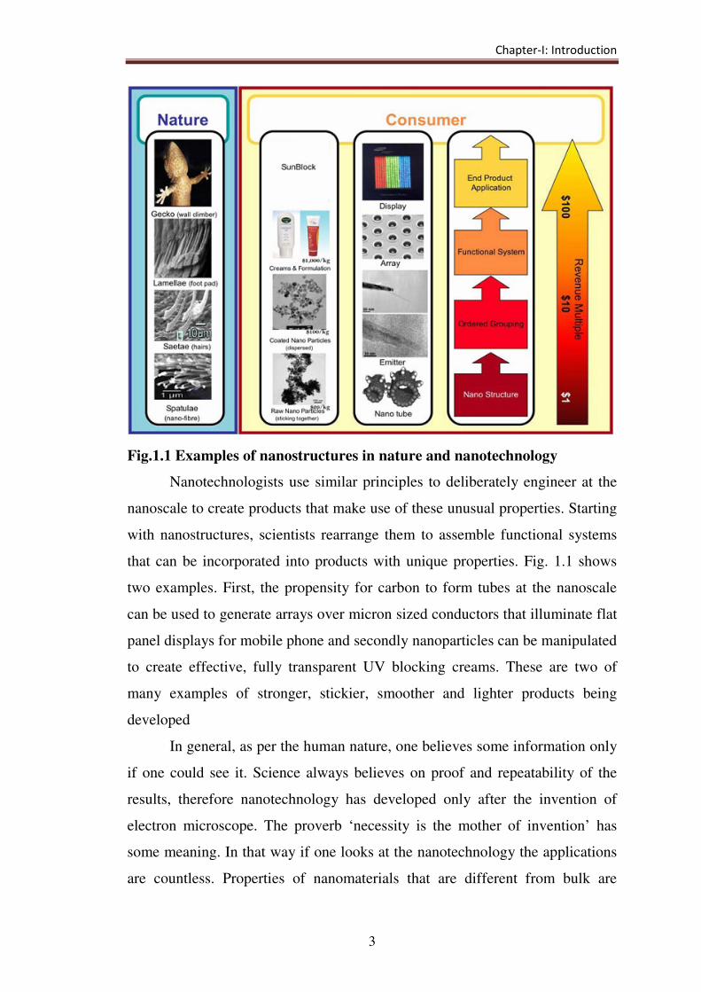
Fig.1.1 Examples of nanostructures in nature and nanotechnology
Nanotechnologists use similar principles to deliberately engineer at the
nanoscale to create products that make use of these unusual properties. Starting
with nanostructures, scientists rearrange them to assemble functional systems
that can be incorporated into products with unique properties. Fig. 1.1 shows
two examples. First, the propensity for carbon to form tubes at the nanoscale
can be used to generate arrays over micron sized conductors that illuminate flat
panel displays for mobile phone and secondly nanoparticles can be manipulated
to create effective, fully transparent UV blocking creams. These are two of
many examples of stronger, stickier, smoother and lighter products being
developed
In general, as per the human nature, one believes some information only
if one could see it. Science always believes on proof and repeatability of the
results, therefore nanotechnology has developed only after the invention of
electron microscope. The proverb ‘necessity is the mother of invention’ has
some meaning. In that way if one looks at the nanotechnology the applications
are countless. Properties of nanomaterials that are different from bulk are
Chapter-I: Introduction
4
variation of the redox properties, band gap variation, enhancement in toughness
and strength, anomalous melting points and unusal crystal structures (in
metals). Nanotechnology is one of the frontier areas of science due to its
versatile applications in various fields.
1.2 History of Nanotechnology and Nanomaterials
The origins of nanotechnology received more attention after 1959, when
Richard Feynman, Physicist and Nobel Prize winner, presented a talk to the
American Physical Society in annual meeting entitled There’s Plenty of Room
at the Bottom [3]. In his talk, Feynman presented ideas for creating nanoscale
machines to manipulate, control and image matter at the atomic scale. In 1974,
Norio Taniguchi introduced the term ‘nanotechnology’ to represent extra-high
precision and ultra-fine dimension, and also predicted improvements in
integrated circuits, optoelectronic, mechanical devices and computer memory
devices [4]. This is the so called ‘top-down approach’ of carving small things
from large structures. In 1986, K. Eric Drexler in his book Engines of Creation
discussed the future of nanotechnology, particularly the creation of larger
objects from their atomic and molecular components, so called ‘bottom-up
approach’ [5]. He proposed ideas for ‘molecular nanotechnology’ which is the
self assembly of molecules into an ordered and functional structure. The
invention of the scanning tunneling microscope by Gerd Binnig and Heinrich
Rohrer in 1981 (IBM Zurich Laboratories), provided the real breakthrough and
the opportunity to manipulate and image structures at the nanoscale.
Subsequently, the atomic force microscope was invented in 1986, allowing
imaging of structures at the atomic scale. Another major breakthrough in the
field of nanotechnology occurred in 1985 when Harry Kroto, Robert Curl and
Richard Smalley invented a new form of carbon called fullerene (buckyballs), a
single molecule of 60 carbon atoms arranged in the shape of a soccer ball. This
led to a Nobel Prize in Chemistry in 1996. Since that time, nanotechnology has
evolved into one of the most promising fields of science, with multi-billion
dollar investment from the public and private sectors and the potential to create

Chapter-I: Introduction
5
multi-trillion dollar industries in the coming decade. The nanomaterials began
immediately after the big bang theory when nanostructures were formed in the
early meteorites. Nature evolved many other nanostructures like seashells,
skeletons etc. Nanoscaled smoke particles were formed during the use of fire
by early humans. The scientific story of nanomaterials however began much
later. One of the first scientific reports is the colloidal gold particles
synthesized by Michael Faraday as early as 1857 [6]. Nanostructured catalysts
have also been investigated over 70 years. By the early 1940’s, precipitated and
fumed silica nanoparticles were being manufactured and sold in USA and
Germany as substitute for ultrafine carbon black for rubber reinforcement [7].
Nanosized amorphous silica particle has found large-scale applications in many
every-day consumer products, ranging from non-dairy coffee creamer to
automobile tires, optical fibers and catalyst support. In the 1960s and 1970s
metallic nanopowders for magnetic recording tapes were developed [8].
Today nanophase engineering expands in a rapidly growing number of
structural and functional materials, inorganic and organic, allowing to
manipulating mechanical, catalytic, electric, magnetic, optical and electronic
properties. The production of nanophase or cluster-assembled materials is
usually based upon the creation of separated small clusters, which are fused
into a bulk material such as nanophase silicon, which differs from normal
silicon in physical and electronic properties, could be applied to macroscopic
semiconductor processes to create new devices. For instance, when ordinary
glass is doped with quantized semiconductor ''colloids,'' it becomes a high
performance optical medium with potential applications in optical computing
[9].
1.3 Importance of Nanoparticles
The nanomaterials have created a high interest in recent years by virtue
of their unusual mechanical, electrical, optical and magnetic properties. The
production of nanophase materials is usually based upon the creation of

Chapter-I: Introduction
6
separated small clusters, which are fused into a bulk-like material. Some
examples are given below:
(a) Nanophase ceramics are of particular interest because they are more ductile
at elevated temperatures as compared to the coarse-grained ceramics.
(b) Nanostructured semiconductors are known to show various non-linear
optical properties. Semiconductor quantum dot particles also show quantum
confinement effects which may lead to special properties, the luminescence in
silicon powder and silicon germanium quantum dots as infrared optoelectronic
devices.
(c) Nanosized metallic powders have been used for the production of gas tight
materials, dense parts and porous coatings. Cold welding properties combined
with the ductility make them suitable for metal-metal bonding especially in the
electronic industry.
(d) Single nanosized magnetic particles are mono-domains and one expects that
also in magnetic nanophase materials that grains correspond with domains,
while boundaries on the contrary to disordered walls. Very small particles have
special atomic structures with discrete electronic states, which give rise to
special properties in addition to the super-paramagnetism behaviour. Magnetic
nanocomposites have been used for mechanical force transfer (ferrofluids), for
high density information storage and magnetic refrigeration.
(e) Nanostructured metal clusters and colloids of mono or plurimetallic
composition have a special impact in catalytic applications. They may serve as
precursors for new type of heterogeneous catalysts which have been shown to
offer substantial advantages concerning to activity, selectivity and lifetime in
chemical transformations and electrocatalysis (fuel cells). Enantioselective
catalysis were also achieved using chiral modifiers on the surface of nanoscale
metal particles.
(f) Nanostructured metal-oxide thin films are receiving a growing attention for
the realization of gas sensors (NOx, CO, CO2, CH4 and aromatic hydrocarbons)
with enhanced sensitivity and selectivity. Nanostructured metal-oxide (MnO2)
finds application for rechargeable batteries for cars and consumer goods.
Chapter-I: Introduction
7
Nanocrystalline silicon films for highly transparent contacts in thin film solar
cell and nano-structured titanium oxide porous films for its high transmission
and significant surface area enhancement leading to strong absorption in dye
sensitized solar cells.
(g) Polymer based composites with a high content of inorganic particles
leading to a high dielectric constant are interesting materials for photonic band
gap structure.
It has been realized that materials in nanodimensions exhibit properties
very different from their bulk counterparts. Increasing knowledge about the
unique properties of nanoparticles has lead to renewed interest in them for
potential applications. The applications of nanoparticles extend to wide-ranging
areas such as catalysis, biosensors, diagnostics, cell labeling, solar cells, fuel
cells, photonic band gap materials, single electron transistors, nonlinear-optical
devices and surface enhanced Raman spectroscopy. The realization of their
various potential applications is only limited by our imagination.
Our focus has been on the production processes rather than on those
which utilize nanoparticles to manufacture other products. Our view of a
production process includes synthesis, in which the material is formed, and
recovery in which the product is collected, modified, divided and packed for
dispatch. Since these are new materials, most of the research and industry effort
is on the development of processes and materials and scale-up of these
processes to industry scale. As understanding about the properties of a new
material increase, effort will tend to shift towards applications and more
exposures might be expected. Secondly, in the early stages of the life cycle of a
new material, many of the potential applications will be speculative and may
never come to fruition.
1.4 Morphology of Nanoparticles
As the particle size ranging from 1 to 100 nm shows unusal properties of
materials. From the literature survey it is seen that ZnO nanowires are used to
sense the ethanol in the range of 1 to 100 ppm, V2O5 nanofibres shows
Chapter-I: Introduction
8
extremely high sensitivity for 1-butylamine and moderate sensitivity for
ammonia. The optical properties of metal nanoparticles have received attention
for making use of them in optical sensors, colour glasses and
photoelectrochemical cells. Metal nanowires and nanoparticles are used in the
nanocircuits. In medicine, gold nanoparticles are utilized for drug delivery and
identification of affected cells. It is important that the only triangular
nanoparticles can be easily identified the cancer cells. Since, they posses sharp
edges, they easily penetrate the cancer cells and the cancer cells can be
destroyed using the same. The most of triangular particles are bound to cell,
they will be killed using far IR radiation. It is also reported that in particular,
nanorods, nanowires, cuboids are showing enhanced photocatalytic activity
than the spherical size.
1.5 Methods for Synthesis of Metal Oxide Nanoparticles
Mainly two approaches have been used for the synthesis of
nanomaterials. Top–down and Bottom–up are the two approaches. Top–down
approach involves mainly physical methods where a bulk material is sliced into
pieces till the desired size is achieved. Lithographic techniques, laser induced
chemical etching and ball milling fall in to this category. However, these
methods are effective only down to the micrometer level. Reaching nanometer
scale makes these methods more expensive and technically difficult. The
bottom–up approaches mainly involve chemical and biological methods to
make nanoparticles. These involve controlled condensation of solute molecules
that is formed during a chemical reaction. The restriction of the condensation
or the growth leads to the formation of particles of desired size and shape [2].
However unlike the chemical synthesis of molecules of a desired structure, the
synthesis of nanomaterials with uniform size and shape is difficult. Thus, large
scale synthesis of nanomaterials remains a challenge.
The development of systematic studies for the synthesis of oxide
nanoparticles is a current challenge and, essentially, the corresponding
preparation methods may be grouped in two main streams based upon the

Chapter-I: Introduction
9
liquid-solid and gas-solid nature of the transformations [10]. Liquid-solid
transformations are possibly the most broadly used in order to control
morphological characterstics with certain “chemical” versatility and usually
follow a “bottom-up” approach. A number of specific methods have been
developed, amongst them those which are broadly in use are given below.
I) Co-Precipitation Method
This involves dissolving a salt precursor in water (or other solvent) to
precipitate the hydroxide form with the help of a base. However, the use of
surfactants, sonochemical methods, and high-gravity reactive precipitation
appear as novel and viable alternatives to optimize the resulting solid
morphological characteristics [11-12].
II) Sol-Gel Method
The sol-gel method provides a highly useful means of preparing
inorganic oxides [13]. It is a wet chemical method and a multistep process
involving both chemical and physical processes such as hydrolysis,
polymerization, drying and densification. The name sol-gel is given to the
process because of the distinctive viscosity increase that occurs at a particular
point in the sequence of steps. Most of the sol-gel literature deals with
synthesis from alkoxides. The important features of the sol-gel techniques are
better homogeneity compared to the traditional methods, high purity, lower
processing temperature and more uniform phase distribution in
multicomponent systems, better size and morphological control, the possibility
of preparing new crystalline and nanocrystalline materials.
The various steps in the sol-gel technique may or may not be strictly
followed in practice. Thus, many complex metal oxides are prepared by a
modified sol-gel route without actually preparing metal alkoxides e.g. a
transition metal salt solution is converted into a gel by the addition of an
appropriate organic reagent.

Chapter-I: Introduction
10
III) Microemulsion Technique
Microemulsions represent an approach based on the formation of
ternary mixture containing water, surfactant and oil. Metal precursors on water
will proceed precipitation as oxo-hydroxides within the aqueous droplets,
typically leading to monodispersed materials with size limited by the
surfactant-hydroxide contact [14].
IV) Solvothermal Method
In this case, metal complexes are decomposed thermally either by
boiling in an inert atmosphere or using an autoclave with the help of pressure.
A suitable surfactant is usually added to the reaction media to control particle
size growth and limit agglomeration [15]. The solvothermal method uses a
solvent under pressure and temperature above its critical point to increase the
solubility of solids and to speed up reactions of solids. Most materials can be
made soluble in proper solvent by heating and pressurising the system near to
its critical point. Lower supersaturation state can be achieved by this method.
VI) Chemical Vapour Deposition (CVD)
There are a number of CVD processes used for the formation of
nanoparticles, some of them are classical, metalorganic, plasma-assisted, and
photo CVD methodologies [17]. The advantages of this methodology consist of
producing uniform, pure and reproducible nanoparticles and films although
requires a careful initial setting up of the experimental parameters.
VII) Pulsed Laser Deposition (PLD)
Pulsed laser deposition heats a target sample (4000 K) and leads to
instantaneous evaporation, ionization, and decomposition with subsequent
mixing of desired atoms. The gaseous entities formed absorb radiation energy
from subsequent pulses and acquire kinetic energy perpendicularly to the target
to be deposited in a substrate generally heated to allow crystalline growth [18].
Irrespective of the preparation method used to obtain ultrafine nano-
oxides, the studies of nanoparticle preparation yielded compelling evidence

Chapter-I: Introduction
11
concerning the fact that crystallization does not follow a traditional nucleation
and growth mechanism. Although subjected to further assessment, it appears
that the simple idea that a small primary size would be prime nucleation as the
key step of crystallization seems essentially correct and holds certain general
validity, at least in solid-solid crystallization mechanisms. When additional
liquid/gas phase crystallization steps are involved in the final formation of the
nanoparticle, other steps like Ostwald ripening may be also of prime
importance. In any case, a lot of novel insights have been recently uncover in
solid-solid transformations and two main theories describe crystallization to
proceed either by surface (single particle) or interface (two or multiple particle)
nucleation [19].
The primacy of one of them has been postulated to be a function of the
oxide chemical nature and temperature, being presumably surface effects
always predominant at higher temperatures. Both theories mostly received
support from kinetic approaches but very recent analyses sensitive to structural
order in the amorphous precursor materials have demonstrated the key role of
intraparticle local order (below 1 nm) in driving the nucleation temperature
onset in a broad interval of ca. 200 K, showing that the whole crystallization
mechanism of oxide nanoparticles appears only compatible with some kind of
intraparticle, dimensional-restricted (surface) mechanism [20].
VIII) Microwave Assisted Sol-Gel Method
In the last decades, microwave heating has been applied in several areas
as a very effective and non-polluting method of activation. Examples of this
technology are materials processing, industrial and commercial applications,
chemistry and biochemistry, among others. In the electromagnetic spectrum,
the microwave radiation is located between infrared radiation and radio waves.
The wavelengths are between 1mm and 1m with corresponding frequencies in
the range of 300 GHz to 300 MHz. Besides telecommunication and microwave,
radar equipments occupy many of the band frequencies in this region, most
routinely used, for industrial and scientific purposes are imposed by
Chapter-I: Introduction
12
international convention be the 2.45GHz (wavelength of 12.2cm) [21]. The
microwave energy is lying between 1.24 meV to 1.24 µeV.
Microwave is a relatively new technology alternative for materials
processing that provides new approaches for enhancing the material properties
as well as economic advantages through energy saving and acceleration of
product development. Clearly, advantages in utilizing this technology include
penetration of radiation, controlled electric field distributions, rapid heating,
self-limiting reactions and selective and volumetric heating [22]. Depending on
the response to microwave heating, materials can be classified into three
principal groups with respect to their interaction with a microwave field:
transparent or low loss materials where microwaves pass through them without
any losses; conductors which reflect microwaves without any penetration;
absorbing or high loss materials, which absorb microwaves and dissipate the
electromagnetic energy as heat, depending on the value of the dielectric loss
factor. Microwave heating of dielectric materials lies in the ability of the
electric field to polarize the charge of the material where polarization cannot
follow the rapid change of the electric field [23].
Microwave heating offers several potential advantages over
conventional heating for inducing or enhancing chemical reactions. These
include direct microwave interaction with certain classes of molecules,
volumetric heating rather than heat flow through the vessel wall, less waste
heat, increased control over heating rates and the possibility of selective
enhancement of desired reactions. This is particularly attractive in the case of
catalytic reactions, where it may be possible to selectively promote desirable
reactions while suppressing undesirable ones. Also, as a fast, simple and energy
efficient method, microwave synthesis has been developed and is widely used
for the synthesis of zeolites and ceramic materials.
Compared with conventional methods, microwave synthesis has the
advantages of very short reaction times, production of small particles with a
narrow particle size distribution and high purity. These conveniences could be
attributed to fast homogeneous nucleation and ready dissolution of the gel.

Chapter-I: Introduction
13
Unfortunately the exact nature of the interaction of the microwaves with the
reactants during the synthesis of materials is somewhat uncertain and
speculative. However, it is well known that the interaction between dielectric
materials and the microwaves leads to dielectric heating in which electric
dipoles in such materials respond to the applied electric field. In liquids, this
constant reorientation leads to a friction between the molecules, which
subsequently generate heat. Many microwave phenomena are poorly
understood such as non-thermal effects and the superheating effect [21-23].
1.6 Properties of ZnO
1.6.1 Physical Properties
The unique and fascinating properties of II-VI compound
semiconductors have triggered tremendous motivation among the scientists to
explore the possibilities of using them in industrial applications, zinc oxide
(ZnO) is a piezoelectric, dielectric, transparent, semiconducting oxide with a
direct band gap of 3.37 eV at room temperature and a large exciton binding
energy (60 MeV), which is 2.4 times the effective thermal energy (KBT = 25
MeV) at room temperature. This is one of the key parameters that ZnO exhibits
near-UV emission, transparency, conductivity and resistance to high
temperature electronic degradation. In addition, ZnO is the hardest of the II-VI
semiconductors due to the higher melting point (1975°C) and large cohesive
energy (1.89 eV). Physical properties of ZnO are given in Table 1.1.

Chapter-I: Introduction
14
Table 1.1: Physical Properties of ZnO
Sr. No. Properties Value
1 Structure Hexagonal
2 Lattice parameter ‘a’ 3.2495 Å
3 Lattice parameter ‘c’ 5.2069 Å
4 c/a 1.602
5 Density 5.606 g cm-3
6 Stable phase at 300 K Wurtzite
7 Melting point 1975°C
8 Thermal conductivity 0.6 , 1-1.2 µSiemen
9 Static dielectric constant 8.656
10 Refractive index , 2.008, 2.029
11 Energy gap 3.37 eV, direct
12 Exciton binding energy 60 MeV
13 Ionicity 62%
1.6.2 Crystal Structure
Zinc oxide crystallizes in three forms: hexagonal wurtzite, cubic zinc
blende and the rarely observed cubic rock salt. The wurtzite structure is most
stable and thus most common at ambient conditions, shown in Fig.1.2 (a). The
zinc blende form can be stabilized by growing ZnO on substrates with cubic
lattice structure, shown in Fig.1.2 (b). The rock salt NaCl-type structure is only
observed at relatively high pressures ~10 GPa. The hexagonal and zinc blende
ZnO lattices have no inversion symmetry (reflection of a crystal relatively any
given point does not transform it into itself). This and other lattice symmetry
properties result in piezoelectricity of the hexagonal and zinc blende ZnO, and
in pyroelectricity of hexagonal ZnO. The hexagonal structure has a point group
6 mm (Hermann-Mauguin notation) and the space group is P63mc or C6v. The
lattice constants are a = 3.25 Å and c = 5.2 Å, their ratio c/a ~ 1.60 is close to

Chapter-I: Introduction
15
the ideal value for hexagonal cell c/a = 1.633. As in most II-VI materials, the
bonding in ZnO is largely ionic, which explains its strong piezoelectricity. Due
to this ionicity, zinc and oxygen planes bear electric charge (positive and
negative, respectively). Therefore, to maintain electrical neutrality, those planes
reconstruct at atomic level in most relative materials, but not in ZnO because
its surfaces are atomically flat, stable and exhibit no reconstruction.
Fig.1.2 (a) Wurtzite structure of ZnO
Fig.1.2 (b) Zinc blende structure of ZnO

Chapter-I: Introduction
16
1.6.3 Lattice Parameters
Lattice parameters are considered important, when one has to develop
semiconductor devices. There are mainly four factors which determine the
lattice parameters of the semiconductors. (i) Free-electron concentration which
affects the potential of the bottom of conduction band normally occupied by
electrons. (ii) Concentration of impurities, defects and the difference in ionic
radii between these defects and impurities with respect to substituted matrix
ions. (iii) External strains. On the other hand, the strict periodicity of the lattice
is disturbed by many imperfections. These imperfections have a considerable,
controlling influence on mechanical, thermal, electrical and optical properties
of semiconductors. They determine the plasticity, hardness, thermal and
electrical conductivities. Commonly the lattice parameters of any crystalline
material are measured accurately by high resolution X-ray diffraction
(HRXRD). Table 1.2 shows a comparison of measured and calculated lattice
parameters of ZnO, c/a ratio reported by several groups [24-25].
Table 1.2: Measured and calculated lattice constants
Name of the method
Lattice parameter a (Å)
Lattice parameter c (Å)
Ratio of c/a
X-ray diffraction
method. 3.2496 5.2042 1.6018
Powder X-ray
diffraction
method.
3.2501 5.2071 1.6021
Linear
Combination of
Atomic Orbital
(LCAO) method.
3.286 5.241 1.595
Chapter-I: Introduction
17
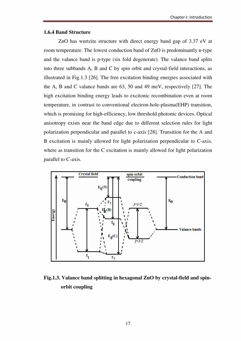
1.6.4 Band Structure
ZnO has wurtzite structure with direct energy band gap of 3.37 eV at
room temperature. The lowest conduction band of ZnO is predominantly n-type
and the valance band is p-type (six fold degenerate). The valance band splits
into three subbands A, B and C by spin orbit and crystal-field interactions, as
illustrated in Fig.1.3 [26]. The free excitation binding energies associated with
the A, B and C valance bands are 63, 50 and 49 meV, respectively [27]. The
high excitation binding energy leads to excitonic recombination even at room
temperature, in contrast to conventional electron-hole-plasma(EHP) transition,
which is promising for high-efficiency, low threshold photonic devices. Optical
anisotropy exists near the band edge due to different selection rules for light
polarization perpendicular and parallel to c-axis [28]. Transition for the A and
B excitation is mainly allowed for light polarization perpendicular to C-axis,
where as transition for the C excitation is mainly allowed for light polarization
parallel to C-axis.
Fig.1.3. Valance band splitting in hexagonal ZnO by crystal-field and spin-
orbit coupling
Chapter-I: Introduction
18
1.6.5 Technology Development
In the field of semiconductor, ZnO is not new, its lattice parameter and
optical properties were studied by Bunn in 1935 and Mallow in 1954. Damen
studied the vibrational properties of ZnO with Raman scattering in 1966 and its
growth though the chemical vapour transport reported by Gali and Coker. ZnO
has been used as LED (1968) and it’s green emission (1969), yellow emission
(1970) are reported by Drapak. The main obstacle for the development of ZnO
has been the lack of reproducibility and low resistivity of p-type ZnO as
recently discussed by Look and Claflin in 2004. The attempt is made to prepare
various morphologies in presence of various oxides mixed with ZnO and to
improve its photo catalytic activity.
1.6.6 Applications of ZnO
As an important low-cost basic II-VI functional semiconductor material,
ZnO has many remarkable applications in functional devices, due to its large
exciton binding energy (60 meV) at room temperature. A great effort has been
paid to the synthesis of ZnO nanostructures, such as nanorods, nanowires [29-
30], nanobelts [31] and nano-tubes [32], which have been attracted intense
attention due to their potential applications in a variety of novel nano-devices,
such as field-effect transistors, single-electron transistors, photodiodes [33] and
chemical sensors [34-36].
The applications of zinc oxide powder are numerous and the principle
ones are summarized below. Most applications exploit the reactivity of the
oxide as a precursor to other zinc compounds. For material science
applications, zinc oxide has high refractive index, high thermal conductivity,
antibacterial and UV-protection properties. Consequently, it is added into
various materials and products, including plastics, ceramics, glass, cement,
rubber, lubricants [37], paints, ointment, adhesive, sealants, pigments, foods,
batteries, ferrites, fire retardants, etc. Zinc oxide is a constituent of cigarette
filters for removal of selected components from tobacco smoke. A filter
consisting of charcoal impregnated with zinc oxide and iron oxide removes
Chapter-I: Introduction
19
significant amounts of HCN and H2S from tobacco smoke without affecting its
flavor. Zinc oxide along with stearic acid is used in the vulcanization of rubber.
Zinc oxide is widely used for concrete manufacturing. Addition of ZnO
improves the processing time and the resistance of concrete against water.
Many sunscreens use nanosized zinc oxide (along with nano titanium dioxide)
because such small particles do not scatter light and therefore do not appear
white. Zinc oxide is added to many food products, for eg. breakfast cereals as a
source of zinc, a necessary nutrient. Zinc white is used as a pigment, in paints
which is more opaque than lithopone, but less opaque than titanium dioxide.
Chinese white is a special grade of zinc white used in artists' pigments. It is
also a main ingredient of mineral makeup. Various plastics, such as
polyethylene naphthalate (PEN), can be protected by applying zinc oxide
coating, the coating reduces the diffusion of oxygen with PEN [38]. Zinc oxide
layers can also be used on polycarbonate (PC) in outdoor applications. The
coating protects PC from solar radiation and decreases the oxidation rate and
photo-yellowing of PC [39]. ZnO has wide direct band gap (3.37 eV).
Therefore, it’s most common potential applications are in laser diodes and light
emitting diodes (LEDs) [40]. Some optoelectronic applications of ZnO overlap
with that of GaN, which has a similar bandgap (~3.4 eV at room temperature).
Compared to GaN, ZnO has a larger exciton binding energy (~60 meV, 2.4
times of the room-temperature thermal energy), which results in bright room-
temperature emission from ZnO. It can be combined with GaN for LED-
applications. For instance as TCO layer and ZnO nanostructures provide better
light outcoupling [41]. Other properties of ZnO favorable for electronic
applications include its stability to high-energy radiation and to wet chemical
etching [42] radiation resistance [43] makes ZnO a suitable candidate for space
applications. ZnO is currently the most promising candidate in the field of
random lasers to produce an electronically pumped UV laser source. The
pointed tips of ZnO nanorods result in a strong enhancement of an electric
field. Therefore, they can be used as field emitters [44]. Aluminium-doped ZnO
layers are used as transparent electrodes. The constituents Zn and Al are much

Chapter-I: Introduction
20
cheaper and less toxic compared to the generally used indium tin oxide (ITO).
One application which has begun to be commercially available is the use of
ZnO as the front contact for solar cells [45]. Transparent thin-film transistors
(TTFT) can be produced with ZnO. As field-effect transistors, they even may
not need a p-n junction [46] thus avoiding the p-type doping problem of ZnO.
Some of the field-effect transistors even use ZnO nanorods as conducting
channels [47]. The piezoelectricity in textile fibers coated in ZnO have been
shown capable of fabricating "self-powered nanosystems" with everyday
mechanical stress from wind or body movements [48-49]. Zinc oxide nanorods
are devices detecting changes in electrical current passing through zinc oxide
nanowires due to adsorption of gas molecules. Selectivity to hydrogen gas was
achieved by sputtering Pd clusters on the nanorod surface. The addition of Pd
appears to be effective in the catalytic dissociation of hydrogen molecules into
atomic hydrogen, increasing the sensitivity of the sensor device. The sensor
detects hydrogen concentrations down to 10 parts per million at room
temperature [50].
1.7 Properties of Cerium Oxide
1.7.1 Physical Properties
Ceria (CeO2) is an oxide with important applications in areas of
catalysis, electrochemistry, photochemistry and materials science [51-55]. Also
it is highly efficient ultraviolet (UV) absorber to protect light-sensitive
materials, as a coating material for protection of corrosion of metals, as an
oxidation catalyst and as a counter electrode for electrochemical devices [56-
59]. The physical properties of CeO2 are represented in Table 1.3. Cerium
oxide has outstanding physical and chemical properties. Recently Zhang et al.
has reported the CeO2 nanocrystal microspheres as a novel adsorbent for the
removal of Cr (VI) from waste water [60]. In its most stable phase, bulk CeO2
adopts a fluorite-type crystal structure in which each metal cation is surrounded
by eight oxygen atoms. The band gap of pure ceria is ~3.2 eV, but crystal

Chapter-I: Introduction
21
defects or impurities can transform the material in a good n-type
semiconductor.
Table 1.3 Physical Properties of CeO2
Sr. No. Properties Value
1) Molar mass 172.115 g/mol
2) Appearance White or pale yellow solid, slightly hygroscopic
3) Density 7.65 g/cm3, solid 7.215 g/cm3, fluorite phase
4) Melting point 2400°C
5) Solubility in water Insoluble
6) Band gap
~3.2 eV
In the area of catalysis, nanoparticles of ceria have been studied since
the early 1970s, but they were poorly characterized. In recent years, substantial
progress has been made and the use of better synthetic methods.
1.7.2 Crystal Structure of CeO2
The fluorite structure is most stable and thus most common at ambient
conditions shown in Fig.1.4. Many researchers were reported the fluorite
structure of CeO2. Small nanoparticles exhibited a nearly amorphous structure
[58, 61-65]. Due to its fluorite structure, the oxygen atoms in a ceria crystal are
all in a plane with one another, allowing for rapid diffusion as a function of the
number of oxygen vacancies. As the number of vacancies increases, the ease at
which oxygen can move around in the crystal increases, allowing the ceria to
reduce and oxidize molecules or co-catalysts on its surface. It has been shown
that the catalytic activity of ceria is directly related to the number of oxygen

Chapter-I: Introduction
22
vacancies in the crystal, frequently measured by using X-ray Photoelectron
Spectroscopy to compare the ratios of Ce3+ to Ce4+ in the crystal.
Fig. 1.4 Fluorite structure of CeO2
1.7.3 Applications of CeO2
Nanostructured metal oxides have attracted considerable attention from
many researchers due to their diversity of applications in various technological
fields of science and technology. Ceria has been used in catalytic converters in
automotive applications. CeO2 possesses many attractive properties that make
it highly promising for a wide range of applications such as solid electrolytes in
solid oxide fuel cells [66], automotive three-way catalyst [67], ultraviolet
absorbers [68-69] and oxygen sensors [70-71]. It is also used as a catalyst for
large-scale fluid cracking in refineries and dehydrogenation of ethyl benzene to
styrene [72] as a sulphur adsorbent for the removal of H2S from hot fuel gas
streams [73]. The reports on the synthesis and applications of coupled
bicomponents ZnO-CeO2 materials are important. The mixed oxide of ZnO
reported that it has high photo catalytic activity due to tuning in the band gap,
which is one of the key concepts for photocatalysis. Therefore we have carried
out this study on microwave assisted process for preparation of ZnO, ZnO-
CeO2 and ZnWO4 nanoparticles and properties of these nanoparticles.

Chapter-I: Introduction
23
1.8 Metal Oxide Nanomaterials
Metal oxides play a very important role in many areas of chemistry,
physics and materials science [74]. The metal elements are able to form a large
diversity of oxide compounds. These can adopt a vast number of structural
geometries with an electronic structure that can exhibit metallic, semiconductor
character [75]. In technological applications, oxides are used in the fabrication
of microelectronic circuits, gas sensors, piezoelectric devices, fuel cells, dye
sensitized solar cells, coatings for the passivation of surfaces against corrosion.
In the emerging field of nanotechnology, a goal is to make nanostructures with
special properties with respect to those of bulk [76-77].
Metal oxide nanoparticles can exhibit unique physical and chemical
properties due to their limited size and a high density of corner surface sites.
Particle size is expected to influence three important groups of basic properties
in any material. The first one comprises the structural characteristics, namely
the lattice symmetry and cell parameters [78]. Bulk oxides are usually robust
and stable systems with well-defined crystallographic structures. However, the
growing importance of surface free energy and stress with decreasing particle
size must be considered. Changes in thermodynamic stability associated with
size can induce modification of cell parameters [79] and in extreme cases the
nanoparticle can disappear due to interactions with its surrounding environment
and a high surface free energy [80].
In order to display mechanical and structural stability, a nanoparticle
must have a low surface free energy. As a consequence of this requirement,
phases that have a low stability in bulk materials can become very stable in
nanostructures. This structural phenomenon has been detected in TiO2, VOx ,
Al2O3 and MoOx oxides [81]. Size-induced structural distortions associated
with changes in cell parameters have been observed in nanoparticles of Al2O3,
NiO, Fe2O3, WO3, MoO3, CeO2, Y2O3 and ZnO [82-84]. As the particle size
decreases, the increasing number of surface and interface atoms generates
stress/strain and concomitant structural perturbations [85-87]. Beyond this

Chapter-I: Introduction
24
“intrinsic” strain, there may be also “extrinsic” strain associated with a
particular synthesis method which may be partially relieved by annealing [88].
Also, non-stoichiometry is a common phenomenon. On the other hand,
interactions with the substrate on which the nanoparticles are supported can
complicate the situation and induce structural perturbations or phases not seen
for the bulk state of the oxide [89].
1.9 Nanomaterials in Semiconductor
The important terms involved in a photoactive semiconductor are
conduction band (CB), valence band (VB), band gap, traps sites and Fermi
level. The bands are the allowed energy states that an electron can occupy in a
material. The highest energy band occupied by an electron is called the valence
band while the next available lowest empty energy level, is called the
conduction band. The bands are clearly differentiated in a semiconductor than a
metal. In case of semiconductor nanoparticles, as the size of the nanoparticles
increases the band gap of the semiconductor decreases, which is shown in
Fig.1.5

Chapter-I: Introduction
25
Fig.1.5 The variation of particle size with band gap energy
The Fermi level is a probability distribution curve that represents a 50%
possibility of locating an electron at a given energy level. For an n-type
semiconductor such as ZnO, TiO2 the Fermi level is close to the conduction
band. Light energy greater than the band gap of the semiconductor excite the

Chapter-I: Introduction
26
electrons from the valence band to the conduction band leaving behind a hole
in the valence band. For example, TiO2 is a large band gap semiconductor and
hence produces e-h pairs on illumination with UV light. The electrons and
holes are available for carrying out redox activities at the semiconductor
surface. Photogenerated e-h pairs are also delocalized in the semiconductor.
These locations are called trap sites (et and ht). The e-h pairs undergo
recombination which results in decreasing the efficiency of the semiconductor.
The numbers of photogenerated electrons in TiO2 are dictated by the ability of
the surroundings to scavenge electrons and holes and the recombination
between the photo generated e-h pairs.
An increase in the band gap of the semiconductor with decrease in the
particle size is defined as quantization effect. Nanoparticles of semiconductors
display unique size-dependent properties (quantization effect) that alter its
photochemical, photophysical, photochromic, optical and electrochemical
responses. Both the large (e.g. ZnO, TiO2, SnO2 and WO3) as well as small
band gap semiconductor (e.g. CdSe and CdS) display this property. Charge
generation, separation, retention and transfer across a semiconductor and its
surroundings is greatly affected due to the quantization effect [90-94]. The
presence of surface bound species which include surrounding electrolytes,
sensitizers like other semiconductors, metals and dyes play an active role in
determining the mechanism of charge transfer taking place at the
semiconductor and surrounding species interface. Photo-induced excitation
leads to charge separation in the semiconductor followed by electron or hole
transfer to the surroundings dictated by the energetics of the system.
Furthermore, defects created in the semiconductor largely depend upon method
and doping. These defects play a vital role in controlling the
photoelectrochemical and photocatalytic behavior of the semiconductor. Two
major drawbacks of any individual large band gap semiconductor have been
identified as, recombination of photogenerated charges (electron and holes) and
limited light harvesting ability. These factors are limiting in the economical
usage of the semiconductor. The former can be minimized by using metal on a

Chapter-I: Introduction
27
semiconductor because metal acts as sink for the electron and decreases
recombination. Sensitization with dyes is one of the most commonly used
methods to overcome the limited light harvesting ability of a large band gap
semiconductor [95]. A semiconductor can be sensitized using another
semiconductor (e.g. TiO2-CdSe) or a dye (Azo dyes) while charge
recombination can be minimized using metal deposits (Ag, Pt). When a metal
is used with a semiconductor, the metal facilitates in decreasing recombination
of the photogenerated charges. Thus both drawbacks of the semiconductor can
be effectively overcome depending upon the material used to create composite
with a semiconductor.
1.10 Impact of Nanomaterials in Catalysis
Nanomaterials are believed to exhibit unique science at nanoscale
regime. The interest in nanomaterials arises from the fact that their physico-
chemical properties are a function of their dimensions. Some of the important
features that influence the catalytic and selectivity are surface structure,
mobility of the active species to restructure as well as the mobility of the
adsorbates on these active species, selective pore size in case of porous
catalysis and metal-support interface sites. In comparison to bulk materials in
nano regime possesses several properties like short range ordering, enhanced
interaction with environments due to high number of dangling bonds, great
variety of the valence band electron structure and self-structuring for optimum
performance in chemisorption and catalysis.
As a consequence of the size reduction, larger portion of their
constituent atoms are located at the surface (surface to volume ratio) and higher
the surface area, higher will be the surface atoms. In general, increase in the
surface area provides more adsorption of reactant molecules on its surface,
which results the higher catalytic activity. Similarly increase in the number of
surface atoms creates more number of active sites, which ultimately result in
higher catalytic activity. In case of fuel cell applications, the current generated
at an electrode is proportional to the active surface of catalysts on the electrode

Chapter-I: Introduction
28
surface, so higher power density fuel cells can be formed from nanomaterials,
because nanomaterials have a higher surface to volume ratio. Researchers have
also shown that the electrolytic properties of the materials are sensitive to
particle size, so increased catalytic activity can be observed for nanoparticles
and nanomaterials. It is important to understand that smaller the particles, the
larger the portion of their constituent at the surface. A surface atom plays an
important role in catalysis, as the reaction takes place at the surface of the
particle. Furthermore, increasing surface area increases the relative contribution
of the surface energy and therefore the thermodynamic stability is decreased
with decreasing particle size [96-97].
Nanomaterials are characterized by a very high number of low co-
ordination number species at edge and corner sites which can provide a large
number of catalytically active sites. Such materials exhibit chemical and
physical properties characteristic of neither that of isolated atoms nor of the
bulk material. The excess surface energy makes the particles more reactive and
structurally sensitive towards their environment. Modern surface science
studies indicate that, during chemisorptions and catalytic reaction, these
particles restructure, and the adsorbed molecules also possesses a high degree
of surface mobility. The adsorbate-induced restructuring facilitates the
breaking of surface chemical bonds and the rearrangement of adsorbates as the
cluster assumes a thermodynamically most stable configuration. As any
materials interact with their environment through solid/gas, solid/liquid, and
solid/solid interfaces, the nanometer scale surface created can be modified to
perform certain functions [98].
Nanosize particles play a crucial role in surface reactivity,
chemisorption and catalysis. Owing to their size, the electronic structure of the
particles significantly differs from that of bulk. The electronic structure of
catalysts has been shown to be important in adsorption and since adsorption is
a necessary step in heterogeneous catalytic reactions, it would be expected that
the changes in the electronic structure would influence the rate of reaction. The
small size also significantly affects the electrochemical behaviour of the

Chapter-I: Introduction
29
nanocrystal materials. Electrochemical model and theories on nanoparticles and
charge-transfer mechanisms for some metal oxide revealed that the properties
of semiconductor gradually transmit to molecular properties as the size of a
crystal is successively decreased in the nanometer range [99]. While going
from bulk to nano size, the semiconductor energy levels become more
separated from each other and the effective band gap increases. As a result of
increase in band gap, the conductivity as well as the density of states in the
conduction and valence band will be reduced. Because of this unusual
behaviour of metals and semiconductors while going from bulk to nano, the
Fermi level and density of states at the interface will alter. Since the Fermi
level is associated with the redox ability of the system, there will be a
considerable change in the rate of redox processes. It would therefore be
possible to control the electrocatalytic and photocatalytic activity of metals and
semiconductors by changing their size [96,100].
1.11 Classification of Nanomaterials Based on its Shape
The main categories of nanoparticle according to shape and the type of
application in which they may be used [101-102] are given in Table 1.4.
Table 1.4 Different shapes of nanoparticles with examples
Morphology of the Nanostructure
Name of the Material
Nanotubes Carbon, (fullerenes)
Nanowires Semiconductors, metals, oxides, sulfides, nitrides
Nanocrystals,
quantum dots
Insulators, semiconductors, metals, magnetic
materials
Other nanoparticles Ceramic oxides
a) Nanotubes
Nanotubes are a particularly novel form of nanoparticle about which
there is great interest and excitement. Carbon nanotubes (CNT) were first

Chapter-I: Introduction
30
discovered by Iijima (1991), and are a new form of carbon molecule. They are
similar in structure to the spherical molecule C60 (buckminsterfullerene)
discovered in the 1980s, but are elongated to form tubular structures 1-2 nm in
diameter [103]. In their simplest form, nanotubes comprise a single layer of
carbon atoms arranged in a cylinder. These are known as single-wall carbon
nanotubes. They can also be formed as multi-wall carbon nanotubes having
diameters significantly greater up to 20 nm and length greater than 1 mm.
CNTs have great tensile strength and are considered to be 100 times stronger
than steel while being only one sixth of its weight thus making them potentially
the strongest. They also exhibit high conductivity, high surface area, unique
electronic properties and potentially high molecular adsorption capacity [104].
Applications which are currently being investigated include; polymer
composites (conductive and structural filler), electromagnetic shielding,
electron field emitters, super capacitors, batteries, hydrogen storage and
structural composites [105]. Hoffman et al. identified four main synthesis
methods for CNTs. These are:
• Laser ablation,
• Arc discharge,
• Chemical vapour deposition (CVD) and
• Plasma-enhanced CVD.
Many of the applications envisaged for CNTs will require bulk
quantities of the material to be produced. For applications where large
quantities of CNTs are required, CVD offers the most suitable approach for
scaling up due to the relatively low growth temperature, high yields and high
purities that can be achieved. Production of relatively large volumes of
unaligned MWCNTs, have been achieved by this and other methods and these
materials are beginning to be used for commercial applications [106].
A recent advance in the development of CNTs is the production of
controlled architectures of aligned CNTs using an injection CVD process. The
CNTs are produced by spraying a solution of ferrocene dissolved in xylene into
a two-stage furnace. The carrier gas is a mixture of argon and hydrogen. The

Chapter-I: Introduction
31
ferrocene decomposes to provide an iron catalyst, which nucleates the nanotube
growth. The xylene acts as the carbon feedstock. The vapour passes into the
second furnace where the nanotubes grow on quartz substrates [107].
One major focus of current research on nanotubes is on scaling-up of
production rates to kilogram quantities. Nanotubes have also been produced
from other materials including silicon and germanium but the development of
various forms and applications for CNTs remain the main focus of activity
[108]. From an occupational hygiene perspective, the large aspect ratios of
CNTs, their durability and the desire to produce bulk quantities make them of
particular interest [109].
b) Nanowires
Nanowires are small conducting or semi-conducting nanoparticles with
a single crystal structure and a typical diameter of a few nanometers and a large
aspect ratio [110]. They are used as interconnectors for the transport of
electrons in nanoelectronic devices. Various metals have been used to fabricate
nanowires including cobalt, gold and copper. Silicon nanowires have also been
produced.
Most approaches to the fabrication of nanowires are derived from
methods currently used in the semi-conductor industry for the fabrication of
microchips. Van Zant (2000) provides a comprehensive review of microchip
fabrication, which makes useful background reading. Typically they involve
the manufacture of a template followed by the deposition of a vapour to fill the
template and grow the nanowire. Deposition processes include electrochemical
deposition and CVD. The template may be formed by various processes
including etching, or the use of other nanoparticles, in particular, the nanotubes
[96,111].
c) Quantum Dots
Quantum dots of semiconductors, metals and metal oxides has the
particle size in all dimension at the forefront of research for the last five years
due to their novel electronic, optical, magnetic and catalytic properties

Chapter-I: Introduction
32
[96,112]. The number of atoms in a quantum dot, which ranges from 1000 to
100,000, makes it neither an extended solid structure nor a single molecular
entity. This has led to various names being attributed to such materials
including nanocrystals and artificial atoms. To date, chemistry, physics and
material science have provided methods for the production of quantum dots
and allow tighter control of affecting factors, for example, particle growth and
size, solubility and emission properties [113].
The majority of research has centred around semiconductor quantum
dots, as they exhibit distinct 'quantum size effects'. The light emitted can be
tuned to the desired wavelength by altering the particle size through careful
control of the growth steps. Various methods can be employed to make
quantum dots however the most common is by wet chemical colloidal
processes [114]. This method gives a better results and the morphology of the
materials.
d) Other Nanoparticles
This catch all category includes a wide range of primarily spherical or
aggregated dendritic forms of nanoparticles. Dendritic forms are where
spherical or other compact forms of primary particles aggregate together to
form chain like or branching structures. Welding fume is the best known
example of this. This “other nanoparticle” category includes existing common
nanoparticles such as ultrafine carbon black and fumed silica which are
synthesized in bulk form through flame pyrolysis methods. Nanoparticles of
this type may be formed from many materials including metals, oxides,
ceramics, semiconductors and organic materials. The particles may be
composites having, for example, a metal core with an oxide shell or alloys in
which mixtures of metals are present. Many of the production processes
involve the direct generation of aerosols through gas phase synthesis, similar to
flame pyrolysis but other production processes including wet chemistry
methods [115]. This group of particles may be categorized as being less well
defined in terms of size and shape, generally larger, and likely to be produced

Chapter-I: Introduction
33
in larger bulk quantities than other forms of nanoparticles. From an
occupational hygiene perspective, the likelihood of aerosol generation and their
availability in bulk quantities makes these nanoparticles of particular interest
[96,116].
1.12 Properties of Metal Oxide Nanoparticles
a) Optical Properties
The optical property is one of the fundamental properties of metal
oxides and can be experimentally obtained from absorption measurements.
While reflectivity is clearly size-dependent as scattering can display drastic
changes when the oxide characteristic size is in the range of photon
wavelength, absorption features typically common and main absorption
behavior of solids [117]. Due to quantum-size confinement, absorption of light
becomes both discrete like and size dependent. For nano crystalline
semiconductors, both linear and non-linear optical properties arise as a result of
transitions between electron and hole discrete or quantized electronic levels
[118]. The effective mass theory (EMA) is the most elegant and general theory
to explain the size dependence of the optical properties of nano-meter
semiconductors, although other theories such as the free exciton collision
model (FECM) or those based on the bond length-strength correlation have
been developed to account for several deficiencies of the EMA theory [119].
Other optical excitations, which showed quantum-size confinement
effects, concern the excitation of optical phonons of oxides. The effects of size
on the phonon spectra of oxide materials have been well established by using
Raman scattering experiments on nanocrystals, in combination with the
theoretical phonon confinement models [120]. Essentially, the phonon
confinement model provides the theoretical background for the study of
nanocrystalline materials and this is the main factor responsible for the changes
observed in the Raman spectrum, which are caused by the size effect. Some
examples of application of the confinement model for qualitative interpretation

Chapter-I: Introduction
34
of Raman results in series of nanostructured oxides like anatase ZnO, TiO2,
CuO, Cr2O3, ZrTiO4, CeO2 or manganese oxides are reported [11-123].
In all cases, “non-stoichiometry” size-dependent defect affects optical
absorption features of nanosized oxides. Typical point defects in
nanostructured oxides concern oxygen or cation vacancies or the presence of
alien’s species, like Cu2+ and Ce3+. Vacancy defects introduce gap states in
proportion to the defect number; in fact, a random distribution of vacancy
defects introduce a Gaussian like density of states which may produce mid-gap
states and be localized near the valence and conduction bands depending on the
electronic nature (donor/acceptor) of the defect and giving characteristic
“localized” features in the UV-Visible spectrum. Such point defects mainly
contribute to the Raman spectra by producing a broadening of the peaks [124].
Alien cations display specific features, like the localized d-d or f-f transitions
of Cu/Ce. Besides electronic modifications, point defects, the alien ions, like
Cu2+ and Ce3+, induce strain and concomitant structural differences in atomic
positions with respect to bulk positions. Strain effects are inherent to
nanostructured materials and may be comprised in the general, ambiguous term
of “surface” effects usually claimed to account for significant deviations in the
confinement theories [125]. Surface effects and, particularly, nonstoichiometry
related to the preparation method are critically important for very low particle
size and to produce characteristic features in the UV-Visible spectrum for
certain oxides such as SnO2 or ZrO2 [96,126].
b) Electrical Properties
Oxide materials can present ionic or mixed ionic/electronic conductivity
and it is experimentally well established that both can be influenced by the
nanostructure of the solid. The number of electronic charge carriers in a metal
oxide is a function of the band gap energy according to the Boltzmann
statistics. The electronic conduction is referred to as n or p hopping type
depending on whether the principal charge carriers are electrons or holes. The
number of “free” electron/holes of an oxide can be enhanced by introducing

Chapter-I: Introduction
35
non-stoichiometry and in such case are balanced by the much less mobile
oxygen/cation vacancies [127]. In an analogous manner to hopping type
conduction, ionic conduction takes place when ions can hop from site to site
within a crystal lattice as a result of thermal activation, and is typically
interpreted on the basis of a modified Fick´s second law. Four mechanism
types have been observed for ionic conduction: direct interstitial, interstitialcy,
vacancy and Grotthus. As charge species (defects; impurities) in polycrystalline
oxides typically segregate to particle boundaries to minimize strain and
electrostatic potential contributions to the total energy, there is a contribution to
the conductivity parallel to the surface which becomes important at the
nanoscale regime [128]. The charge carrier (defect) distribution also suffers
strong modification from bulk materials, as there is presence of charge carriers
through the whole material as a consequence of the shielded electrostatic
potential depletion at surface layers of nanosized materials [129]. As a result of
these nanoscale derived effects, it is well known that CeO2 exhibits an
improved n-type conductivity which may be four order of magnitude greater
than the corresponding to bulk/micro-crystalline ceria and is ascribed to a
significant enhancement of the electronic contribution [130]. Alteration of the
transport properties is also observed in ZrO2 but the physical ground is still far
from being understood [131]. The strong size dependence observed for the
electrical conductance in the context of gas-sensing devices has been recently
reviewed for the SnO2, WO3, and In2O3 oxides. In proton conductors, like
SrCe0.95Yb0.05O3-d enhanced conduction and faster kinetics under H-
atmospheres are observed in nanosized samples as these phenomena are largely
determined by boundary/interfacial effects [132]. Interesting to stress here is
that some of the most dramatic effects of the nanostructure on ionic transport in
oxides are observed in the field of Li+ ion batteries. An outstanding
enhancement in conductivity due to Li+ ion vacancy has been achieved using
Li-infiltrated nanoporous Al2O3 [133].

Chapter-I: Introduction
36
c) Mechanical Properties
Main mechanical properties concern low yield (stress and hardness) and
high (superplasticity) temperature observables. Information on oxide
nanomaterials is scarce and mainly devoted to analyze sinterability, ductility
and superplasticity. These mechanical properties are also found to be strain-rate
dependent; an enhanced strain rate sensitivity at room temperature is observed
for TiO2 and ZrO2 with decreasing primary particle grain size. In spite of such
facts, it is clear that oxide materials (like ZnO, Al2O3, ZrO2, CeO2 and TiO2)
sintered under vacuum or using the spark plasma technique display enhanced
field strength and hardness with respect to conventional or bulk ceramic
materials and have the additional properties of being transparent (films), being
potential materials for the aerospatial industry [134]. Superplasticity refers to
the capacity of oxide materials. Essentially, polycrystalline tetragonal ZrO2
appears as the most celebrated example of a superplasticity ceramic and
together with TiO2, the ZrO2 are the only nano-oxides subjected to studies. At
room temperature, nanocrystalline oxides may have a small amount of ductility
beyond that exhibited by bulk materials but they are not superplastics. At high
temperatures, they seem to exhibit significant compressive ductility and strain
rate sensitivities that indicate superplasticity [135].
d) Chemical Properties
Metal oxides are used for both their redox and acid/base properties in
the context of absorption and catalysis. The three key features essential for
their application as absorbents or catalysts are (i) the coordination environment
of surface atoms, (ii) the redox properties and (iii) the oxidation state at surface
layers. Both redox and acid/base properties are interrelated and attempts can be
found in the literature to establish correlations of both properties. In a simple
classification, oxides having only s or p electrons in their valence orbitals tend
to be more effective for acid/base catalysis, while those having d or f outer
electrons find a wider range of uses [136].

Chapter-I: Introduction
37
The solid in a given reaction conditions that undergoes reduction and
reoxidation simultaneously by giving out surface lattice oxygen anions and
taking oxygen from the gas phase is called a redox catalyst. This process
necessarily demands microscopy reversibility and implies dynamic operation.
The commonly accepted mechanism was developed by Mars van Krevelen and
essentially implies that redox systems require high electronic conduction
cations to manage electrons and high oxygen-lattice mobility. Based on modern
isotopic exchange experiments, the redox mechanism of chemical reactions can
be more specifically divided in (i) extra facial oxygen in which adsorbed
(oxygen) species react (electrophilic reaction) and (ii) interfacial oxygen where
lattice oxygen vacancies are created (nucleophilic reaction) [137]. There are
enormous evidences which exhibit that nucleophilic oxygen is capable of
carrying out selective oxidations while it seems that electrophilic species seems
to work exclusively on non-selective ones. Latter, it was shown that
hydrocarbon selective oxidation starts with H-abstraction steps and that the
filling of oxygen vacancies requires the cooperation of a significant number of
cations. So, typically, an oxidation reaction demands to optimize three
important steps: the activation of the C-H bond and molecular oxygen and the
desorption of products (to limit over-oxidation). The effect of size on these key
steps is unknown but can be speculated to be related to the oxidation state of
surface cations and their ability to manage electrons and the influence of non-
stoichiometry on the gas-phase oxygen species handling and activation [138].
Many oxides also display acid/base properties. Oxide materials can
contain Bronsted and Lewis acid/base sites. Bronsted acid (A) and base (B)
interactions consist of the exchange of protons as HA + B = A- + HB+. In any
solid, two independent variables, the acid/base strength and amount (density
per surface unit) need to be addressed to give a complete picture of its
acid/base characteristics. Such characteristics are basically linked to the nature
(valence/cation size) of the element present in the oxide and general views of
the behavior of Bronsted/Lewis acidity as a function of solid state variables
have been published. Essentially, Lewis acidity is characeristic of ionic oxides

Chapter-I: Introduction
38
and practically absent in covalent oxides. The strongest Lewis acid oxides are
Al2O3 and Ga2O3. As a general rule, for stronger Lewis acid, the few sites are
available (amount) due to the higher level of surface hydroxylation. As
mentioned, Lewis acidity is mostly associated to oxides with ionic character;
Lewis basicity is mostly associated with them. This means that the stronger the
Lewis acid sites, the weaker the basic sites and vice versa. On the contrary,
most of the ionic metal oxides do not carry sufficiently strong Bronsted acidity
to protonate pyridine or ammonia at room temperature although the more acids
of them can do it at higher temperatures. In spite of this, the surface OH groups
of most ionic oxides have a more basic character than acid character. Finally,
strong Bronsted acidity appears in oxides of elements with formal valency five
or higher (WO3, MoO3, N2O5, V2O5 and S-containing oxides) [139].
1.13 Advanced Oxidation Processes
Advanced oxidation processes (AOP’s), uniting together ozone and high
output ultraviolet technologies, in conjunction with hydrogen peroxide and
catalyst are successfully used to decompose many toxic and bio-resistant
organic pollutants in aqueous solution to acceptable levels, without producing
additional hazardous by-products or sludge which require further handling.
Advanced oxidation processes involve the generation of hydroxyl (•OH)
radicals which oxidize the pollutants. Advanced oxidation processes can be
broadly classified into the following groups:
i) Homogeneous photocatalysis,
ii) Heterogeneous photocatalysis
i) Homogeneous photocatalysis
The applications of homogeneous photodegradation (single-phase
system) to treat contaminated water, involves the use of an oxidant to generate
radicals, which attack the organic pollutants to initiate oxidation. The major
oxidants used are: Hydrogen peroxide (UV /H2O2), Ozone (UV /O3),
Hydrogen peroxide and Ozone (UV /O3/ H2O2),

Chapter-I: Introduction
39
Photo-Fenton system (Fe+3 / H2O2).
ii) Heterogeneous photocatalysis
Heterogeneous photocatalytic process consists of utilizing the near UV
radiation to photo-excite a semiconductor catalyst in the presence of oxygen.
Under these circumstances oxidizing species, either bound hydroxyl radicals or
free holes, are generated as shown in Fig.1.6. Using photocatalysis, organic
pollutants can be completely mineralized reacting with the oxidizers to form
CO2, water and dilute concentration of simple mineral acids. The process is
heterogeneous because there are two active phases, solid and liquid. This
process can also be carried out utilizing the near part of solar spectrum (λ <
380nm) which transforms into a good option to be used [140].
Fig.1.6 Scheme showing some of the events that might be taking place on an irradiated semiconductor particle

Chapter-I: Introduction
40
The semiconductor may be in the form of a powder suspended in the
water or fixed on a support. The most active photocatalyst for this application
is the anatase form of TiO2/ZnO because of its high stability, good performance
and low cost [141].
1.14 History and Current Status of Photocatalysis
Environmental pollution and energy shortage, being regarded as the top
two challenges facing mankind in the next 50 years, have attracted much
attention from both government agencies and scientific communities.
Semiconductor based heterogeneous photocatalytic technology was developed
as a promising solution to the two challenges. The utilization of
semiconductors as a photocatalyst started from the first report by Fujishima and
Honda in 1972 [142]. At that time, the energy crisis was spreading around the
world, the water splitting into hydrogen and oxygen under ultraviolet (UV)
irradiation by using TiO2 photoanode inspired extensive research concerning
solar energy conversion and created a new era in the field of photocatalyst. In
1977, Bard reported that CN- was photocatalytically oxidized into OCN- on
TiO2 [143] and the applications of photocatalysis were extended into the field
of waste water treatment and environmental remediation. Since the beginning
of the 1990s, environmental pollutants have aroused increased public concern.
Heterogeneous photocatalytic reactions on ZnO nanoparticles (n-type
semiconductors) are now recognized as an ideal technology for removal of all
kinds of pollutants both in water and air [144-148]. Most of the investigations
have focused on mixed-metal oxides which show relatively high reactivity and
chemical stability under ultraviolet (UV) light.
Over the last 10 years the scientific and engineering interest in the
application of semiconductor photocatalysis has grown exponentially. In the
areas of water, air and waste water treatment the photocatalysis by metal oxides
has many potential applications as an environmental control technology [149].
Many background information reviews on photocatalysis have been appeared
in the literature, note worthy recent reviews are provided by Ollis and Al-
Chapter-I: Introduction
41
Akabi, [150] Blake, [151] Mills et al., [152] Bahnemann et al. [153] Pichat,
[154] Aithal et al., [155] and Lewis [156].
Semiconductor photocatalysis with a primary focus on TiO2 as a durable
photocatalyst has been applied to a variety of problems of environmental
interest in addition to water and air purification. It has been shown to be useful
for the destruction of microorganisms such as bacteria [157] and viruses [158].
Semiconductors (e.g., TiO2, ZnO, Fe2O3, CdS and ZnS) can act as sensitizers
for light-reduced redox processes due to their electronic structure, which is
characterized by a filled valence band and an empty conduction band [159].
The approaches also include the incorporation of transition metals doping [160-
163]. Spinel zinc ferrite (ZnFe2O4) is a narrow band gap semiconductor that has
a potential application in the conversion of sunlight, because of its sensitivity to
ultra-violet light and no photochemical corrosion [164]. In contrast, on bulk
semiconductor electrodes only one species, either the hole or electron, is
available for reaction due to band bending [165]. However, in very small
semiconductor particles and suspensions both species are present on the
surface. Therefore, careful consideration of both the oxidative and the reductive
paths is required.
1.15 Literature Survey
The fine powders of oxides have been prepared by many methods,
including forced hydrolysis, sol-gel, hydrothermal, co-precipitation, surfactant
templating and spray pyrolysis [166]. However, microwave-assisted synthesis
is very beneficial to find a fast, simple and energy efficient approach to
produce fine metal oxide nanoparticles [167]. Microwave assisted synthesis is
relatively new technology to produce inorganic compounds since 1986 for
materials processing to enhance the material properties as well as economic
advantages [168]. Microwave heating offers several potential advantages over
the conventional heating for inducing or enhancing chemical reactions [169].
These includes direct microwave interaction with certain class of molecules,
volumetric heating rather than heat flow through the vessel wall, less waste
Chapter-I: Introduction
42
heat, increased control over heating rates and the possibility of selective
enhancement of desired reactions [170]. Microwave synthesis has been
developed and widely used for the synthesis of zeolites and ceramic materials.
Compared with conventional methods, microwave synthesis has advantages: 1)
Production of small particles with a narrow size distribution with high purity
and 2) within very short reaction time. These conveniences could be attributed
to fast homogeneous nucleation and ready dissolution of the gel [171].
Microwave heating is in situ mode of energy conversion therefore it is very
attractive for chemist due to its simplicity and cost effective technique.
A number of methods have been used for synthesizing ZnO
nanopowders [172-178] and in recent years, a new method has been reported as
microwave-assisted synthesis. Due to its unique features such as short reaction
time, enhanced reaction selectivity, energy saving, and high reaction rate [179],
the application of microwave-assisted synthesis of ZnO nanoparticles has been
rapidly growing [179-183]. Many methods have been reported for the synthesis
of ZnO nanoparticles, including the sol-gel [184], microwave method [185],
evaporative decomposition of solution [186], template-assisted growth [187],
wet chemical synthesis [188] and gas-phase reaction [189]. Some researchers
have been highlighted the performance of ZnO for degradation of some organic
compounds [190-191]. In addition, ZnO has more functions than TiO2 [192]
and recent researches have pointed out that ZnO can also be used in the acidic
or alkaline conditions through the proper treatment [193-194].
Hong et al., [195] reported the synthesis of Zinc oxide (ZnO)
nanoparticles using zinc nitrate and NaOH by ultrasonic irradiation technique
at room temperature. The ZnO nanoparticles were heated individually in an
electric furnace for two hours at 700°C. The morphology and optical
properties of the C60 and ZnO nanoparticles were characterized by X-ray
diffraction, SEM, transmission electron microscopy and UV-Visible
spectroscopy. The photocatalytic activity of the heated and unheated C60 and
ZnO nanoparticles were studied for the decomposition of Methylene blue,
Methyl orange and Rhodamine B.
Chapter-I: Introduction
43
Comparison of dye degradation efficiency using ZnO powders with
various sizes reported by Wang et al., [196]. ZnO powders with various size
scales (mean diam.size: 10, 50, 200, and 1000 nm) were prepared by two
different preparation methods, thermal evaporation method and chemical
deposition method. The size 50 nm prepared by thermal evaporation method
shows the highest photocatalytic activity. In addition the tetrapod ZnO
nanopowders had the higher efficiency than irregular ZnO nanoparticles.
However, the smallest 10 nm ZnO nanoparticles prepared by chemical
deposition method and the degradation efficiency was discussed through the
photocatalytic experiments using 50 nm ZnO nanoparticles as photocatalyst.
Giraldi et al., [197] reported annealing effect on photocatalytic efficiency of
ZnO nanoparticles prepared by chemical technique. The samples were annealed
and effects on the photocatalytic properties, surface decontamination and the
consequent particle change, in terms of crystallinity are studied. The as-
prepared samples correspond to a metastable phase (oxy or hydroxy zinc
acetate) and post annealing leads to ZnO crystals. The XRD patterns showing
only the ZnO phase for heat treatment at 100°C, FTIR data shows that
carboxylate group remains attached to the ZnO surface up to 300 °C. Up to
300 °C the presence of these carboxylate groups, provided by the synthesis
method, showed to be more relevant to photoactivity than the specific surface
area. At higher temperatures, crystallinity becomes the dominant factor and an
increasing of crystallinity favors the photoactivity.
The study of photoconductivity and photoluminescence of ZnO
nanoparticles is reported by Kripal et al., [198]. They studied the
photoconductvity and photoluminescence properties of ZnO nanoparticles
(NPs) prepared by using co-precipitation method and thioglycerol as a caping
agent and annealed at 300°C. The TEM and XRD pattern confirm the
hexagonal wurtzite structure of ZnO nanoparticles. The UV-Visible absorption
spectrum of ZnO NPs shows blue shift of absorption peak as compared to bulk
ZnO. The photoluminescence (PL) spectra of as-synthesized ZnO NPs show
band edge emission as well as blue-green emission.

Chapter-I: Introduction
44
Growth and gas sensing properties of p and n-type ZnO nanostructures
are reported by Ramgir et al.,[199]. ZnO nanoparticles (NPs) of 5 to15 nm size
and nanowires (NWs) of 50 to100 nm diameter were prepared using simple
chemical method, exhibiting p and n-type characteristics, respectively. ZnO
NW-films show good sensitivity and selectivity towards H2S in ppm range with
fast response and recovery times. Interestingly, ZnO NP-films showed p-type
conductor.
Sun et al.,[200] reported on bar-like nano ZnO prepared by
hydrothermal method at 230°C using ZnSO4 and CO(NH2)2 as the materials
and CTAB as the surface active agent. The XRD shows that the nanoparticles
of ZnO have hexagonal wurtzite structure. The observed results by SEM
shows that the products showed rod-like morphology with average diameter of
about 60-80 nm and length of about 260-580 nm. Methylene blue in aqueous
solution could decompose rapidly under photocatalysis of bar-like nano ZnO
when pH value of the solution was 8.0 and the degradation rate of Methylene
Blue reached 100% after 90 minutes.
Dalai et al., reported [201], hollow ZnO microspheres with interior
diameter of ∼10 µm were synthesized by a facile solution method using
polymethyl methacrylate (PMMA) microspheres as template. The hollow
microspheres are built by layers of nanoparticles with high crystallinity. The
shell thicknesses are ∼100 nm. The XRD, SEM, TEM and XPS measurements,
a possible formation mechanism for the hollow ZnO microspheres is discussed.
As-synthesized hollow ZnO microspheres exhibit novel absorption band in the
region of UV. Band gap of the hollow ZnO microsphere is 3.53 based on its
UV-Visible absorption spectrum.
The study of photochemical properties of CeO2-coated ZnO nanorods
were carried out by Lau et al., [202]. Well-aligned ZnO nanorods were
deposited by a mild hydrothermal process and coated with nanosized CeO2
particles (∼5 nm) by an oxidative-soak-coating method at 45° C. The low
growth temperature proved useful in avoiding interfacial reaction between the
two phases. Correlation of photoluminescence results indicated that the defects

Chapter-I: Introduction
45
responsible for the deep level emission (DLE) from ZnO were largely located
at the surface. The CeO2 coating reduced the DLE but also the photocatalytic
activities as surface hydroxyl groups were involved in the nucleation of the
CeO2 phase. Wang et al., [203] reported the hydrothermal process for CeO2-
ZnO composite nanostructure, by using Zn (NO3)2·6H2O, Ce (NO3)3·6H2O and
hexamethylenetetramine on Si substrate at 90°C. The structures, morphologies
and the composite of CeO2/ZnO samples have been investigated by XRD,
TEM, SEM and EDX at room and it shows that the obtained CeO2/ZnO
composite nanostructures have different morphology for composite. The result
shows that the uniform and dense CeO2 nanoparticles cover the whole surface
of single crystal ZnO rods when the Ce3+/Zn2+ molar ratio of reaction solution
is 1/10. This kind of the CeO2/ZnO composite nanostructure may find potential
application in the selective detection of CO.
Wu et al., [204] developed a layer-by-layer (LBL) assembly approach to
synthesize ZnO nanorod-based hybrid nanomaterials such as ZnO/CeO2,
ZnO/CdS and ZnO/Ag on ZnO nanorod templates at room temperature. The
ZnO nanorod-based hybrid nanomaterials have been characterized by TEM,
HRTEM, XRD and XPS. It is indicated that a uniform coating layer consisting
of homogeneous nanoparticles is deposited on the surface of ZnO nanorods due
to the strong electrostatic attraction between metal ions and polyelectrolyte
modified ZnO nanorods. The general approach presented here can be extended
to the synthesis of other one-dimensional (1D) nanostructure-based hybrid
Nanomaterials.
CeO2/ZnO nanostructured microspheres as catalysts for the oxidative
coupling of CH4 with CO2, the conversion of CH4 corresponded with that using
the CeO2/ZnO nanoparticles observed by Yongjun et al., [205]. CeO2/ZnO
nanostructured microspheres with an average diameter of ≈3.8 µm were
sysnthesized by a solid-stabilized emulsion technique. The CeO2/ZnO
nanostructured microspheres were characterized with SEM, XRD, CO2-TPD,
BET measurement. Based on the oxidative coupling reaction of CH4 with CO2
as an oxidant, the catalytic performance of the CeO2/ZnO nanostructured

Chapter-I: Introduction
46
microspheres was evaluated and compared with that of the CeO2/ZnO
nanoparticles. The surface of the CeO2/ZnO nanostructured microspheres
consisted of petal-like structures with a petal thickness of ≈90 nm and a petal
depth of 0.4-0.9 µm. Using CeO2/ZnO nanostructured microspheres as
catalysts for the oxidative coupling of CH4 with CO2, the conversion of CH4
corresponded with that using the CeO2/ZnO nanoparticles, while the CeO2/ZnO
nanostructured microspheres had much longer operating life.
ZnWO4 as a kind of tungstate has received considerable attention due to
its applications as an X-ray and γγγγ-scintillator, photoanodes and solid-state laser
host, as well as for acoustic and optical fibers reported by Montini et al. [206].
Tungstates of divalent transition metals (MIIWO4, M=CoII, NiII, CuII, ZnII) were
prepared by reaction of transition metal nitrates with sodium tungstate. The
precipitates were then calcined at 500ºC. The materials were characterized by
means of ICP-AES, UV, XRD, SEM and surface area analysis. The higher
activity for the decolorization of Methylene Blue (MB) and Methyl Orange
(MO) of ZnWO4 compared to that of the other investigated tungstates was
correlated with its strong tendency of excitons self-trapping.
The enhanced photocatalytic performance was observed by Huang et al.,
[207] ZnWO4 nanoparticles prepared by hydrothermal technique with different
annealing temperature and time. The high photocatalytic activity confirmed by
degradation of formaldehyde and RhB in gaseous and water respectively. The
highest photocatalytic activity both appeared at 450°C for 1 h. The
photocatalytic activity of ZnWO4 was a little higher than that of P-25
(Degussa) in gaseous phase and lower in aqueous.
Jia et al., [208] reported the structural and optical properties of ZnWO4
and CdWO4 nanofilms by a novel route through the combination of reverse
micelle system with dip-coating technology. Here collodion is used as a
dispersant and film-forming agent to obtain nanofilm with a good quality films.
The SEM and XRD results indicate ZnWO4 and CdWO4 nanoparticles with
monoclinic system and wolframite structure. The nanofilm's PL bands shows
blue shift compared with bulk materials where as red shift compared with
Chapter-I: Introduction
47
nanoparticles. FTIR absorption bands between 400 and 900 cm-1 prove the
presence of ZnWO4.
Wang et al., [209] used a microwave assisted sol-gel method. The
results indicate the cubic fluorite structure. TEM reveals that the size of
crystalline particles of 4 to 6 nm. Preparation of monodisperse cerium oxide
nanoparticles were carried out by Soucek et al. [210]. The products were
characterized by Raman spectroscopy, XRD, UV-Visible spectroscopy and
TEM. The TEM images and UV-Visible spectra show that the CeO2 particles
prepared are uniform nanosized and absorb UV light in the range of 250 t0 400
nm. The sizes of the nanoparticles were obtained about 5 to 20 nm.
Zhang et al. [211] synthesized hierarchical CeO2 nanocrystal
microspheres by sol-gel method at of 120°C temperature. The product was
characterized by XRD, TEM and clearly revealed the microstructure of the
CeO2 nanospheres. These nanospheres are of porous structure and 50 to 100 nm
in diameter. Photocatalytic degradation of various dyes with different
chromophores such as Methyl Violet, Methylene Blue and Rhodamine B by
using titanium oxide was reported by Hosseinnia et al. [58]. They have been
synthesized single phase anatase titania powders by a simple precipitation
method. The powders were characterized by XRD, TEM and surface area, after
calcinations at 550°C for 3 hrs. TEM results show the particle size about 20 nm
and surface area of 75 m2/g. From the detailed literature survey it is seen that
very few scientists have been given attention for the semiconductors like ZnO,
ZnWO4, CeO2 and ZnO-CeO2 by using microwave assisted method. Therefore
it has an advantage of very short reaction time, production of small particles
with a narrow size distribution and high purity. These conveniences could be
attributed to fast homogeneous nucleation and ready dissolution of the gel.
Microwave heating is in situ mode of energy efficient method.
1.16 Plan of the Research Work
From the industrial point of view, it is of prime importance to use new
materials as a photocatalyst. Metal oxide nanomaterials are the benign catalyst.

Chapter-I: Introduction
48
The metal oxide nanoparticles as a photocatalyst are supposed to modify the
route of chemical reaction thereby reducing the cost of production.
Photodegradation of hazardous organic compounds like dye and pesticides
from industrial effluents is of prime importance and at ease can be done by
metal oxide nanoparticles within shorter duration due to its large surface to
volume ratio.
It is observed from the literature survey that mixed oxides are more
favourable than single oxides due to its increase in surface area, tuning of the
band gap of energy, which is required for photocatalyst.
The important task of the present work is to prepare ZnO and its mixed
oxides such as ZnO-CeO2 and ZnWO4 by using very simple microwave
assisted sol-gel method. The properties such as crystal structure, catalytic and
spectral properties are greatly influenced by the metal ions present at two
different sites. Therefore, to find out the effect of substitution of different metal
ions on the properties of metal oxide, various techniques such as scanning
electron microscopy (SEM), transmission electron microscopy (TEM), electron
dispersive X–ray analysis (EDS), X–ray diffraction analysis (XRD), thermo-
gravimetric analysis (TGA), Differential thermal analysis (DTA), UV-Visible
spectroscopy and IR spectroscopy are used. The microwave assisted method is
employed for the synthesis of zinc oxide, ZnO-CeO2, and ZnWO4. The ZnO
and mixed ZnO with CeO2 and WO3 are tested for the photodegradation of dyes
such as Methyl Orange, Methylene Blue and Rhodamine B. The effect of
catalyst loading, pH and initial concentration of dyes on the photocatalytic
degradation efficiency using ZnO and mixed ZnO nanorods as a photocatalyst
was tested.
Chapter-I: Introduction
49
1.17 References
[1] H. Bam ford, Curr. Biol., 10 (2000) 558.
[2] G. M. Whitesides, Small, 1 (2005) 172.
[3] R. Feynman There’s Plenty of Room at the Bottom. An Invitation to Enter a
New Field of Science, lecture, annual meeting of the American Physical
Society, California Institute of Technology, 29 (1959).
[4] N. Taniguchi, On the Basic Concept of 'NanoTechnology', Proc. Intl. Conf.
Prod. Eng. Tokyo, Part II, Japan Society of Precision Engineering, (1974).
[5] K. E. Drexler, Engines of Creation, Anchor Press, New York, (1986).
[6] J. R. Morones, J. L. Elechigeurra, A. Camacho, K. Holt, J. B. Kouri, J.
T. Ramirez, M. Yacaman, J. Nanotechnology, 16 (2005) 2346.
[7] A. Roucoux, J. Schulz, H. Patin, Chem. Rev., 102 (2002) 3757.
[8] E. A. Heins, Z. S. Siwy, L. A. Baker, C. R. Martin, Nano Lett., 5
(2005)1824.
[9] B. Viswanathan, Nano Materials, Narosa Publishing House, (2009).
[10]V. Uskokovick, M. Drofenik, Surf. Rev. Letter, 12 (2005) 239.
[11] M. Fernandez-Garcia, X. Wang, C. Belver, J. C. Hanson, J. A. Rodriguez,
J. Phys. Chem.C, 111 (2007) 674.
[12] H. Zhang, J. F. Bandfield, J. Phys. Chem. C, 111 (2007) 6621.
[13] M. Fernandez-Garcia, C. Belver, X. Wang, J.C. Hanson, J.A. Rodriguez,
J. Am. Chem.Soc.,55 (2007) 73.
[14] K. Bougrin, A. Loupy, M. Soufiaoui, J. Photochem. Photobio. C:
Photochem. Rev., 6 (2005) 139.
[15] H. S. Ku, F. Siu, E. Siores, J. A. R. Ball, J. Mater. Proc. Tech.,
139 (2003) 291.
[16] M. Al-Harahsheh, S. W. Kingman, Hydrometallurgy,73 (2004) 189.
[17] B. J. Scott, G. Wirnsberger, G. D. Stocky, Chem. Mater., 13 (2001) 3140.
[18] I. Yoffre, Adv. Phys., 1 (2001) 50.

Chapter-I: Introduction
50
[19] Y. D. Glinka, S. H. Lin, L. P. Hwang, Y. T. Chen, N. H. Tolk, Phys. Rev.
B, (2001) 85421.
[20] L. K. Pan, C. Q. Sun, J. Appl. Phys., 95 (2004) 3819.
[21] M. Iwamoto, T. Abe, Y. Tachibana, J. Mol. Catal. A, 55 (2000) 143.
[22] L. Combemale, G. Caboche, D. Stuerga, D. Chaumont, Microwave
Research Bulletin, 40 (2005) 529.
[23] K. Borgohain, N. Morase, S. Mahumani, J. Appl. Phys., 92 (2002) 1292.
[24] Ü. Özgür, Ya. I. Alivov, C. Liu, A. Teke, M. A. Reshchikov, S. Dogan, V.
Avrutin, S. J. Cho, H. Morkoçd, Journal of Appl. Phys., 98 (2005) 041301.
[25] L. M. Angelats, Ph.D thesis, University of Puerto Rico (UPR), (2006).
[26] A. Mang, K. Reimann, S. Rubenke, Solid State Communication, 94 (1995)
51.
[27] Y. S. Park, C. W. Litton, T. C. Collins, D. C. Reynolds, Phys. Rev.,143
(1996) 512.
[28] H. Yoshikawo, S. Adachi, Jpn. J. Appl. Phys., 36 (1997) 6267.
[29] K. Raidongia, C. N. R. Rao, J. Phys. Chem. C, 112 (2008) 13366.
[30] J. Yang, W. Z. Wang, Y. Ma, D. Z. Wang, D. Steeves, B. Kimball, Z. F.
Ren, J. Nanosci. Nanotechnol., 6 (2006) 2196.
[31] Z. W. Pan, Z. R. Dai, Z. L. Wang, Science, 291 (2001) 1947.
[32] G. W. She, X. H. Zhang, W. S. Shi, X. Fan, J. C. Chang, C. S. Lee, S. T.
Lee, C. H. Liu, Applied Physics Letters, 92 (2008) 053111.
[33] J. P. Cheng, Y. J. Zhang, R. Y. Guo, J. Crystal Growth, 310 (2008) 57.
[34] Y. J. Chen, C. L. Zhu, G. Xiao, Sensors and Actuators B, 129 (2008) 639.
[35] T. J. Hsueh, S. J. Ch, C. L. Hsu, Y. R. Lin, I. C. Chen, J. Electrochem.
Soc.,155 (2008) 1520.
[36] Y. S. Zhang, K. Yua, D. S. Jiang, Z. Q. Zhua, H. R. Geng, L. Q. Luo,
Applied Surface Science, 242 (2005) 212.
[37] A. Hernandezbattez, R. Gonzalez, J. Viesca, J. Fernandez, J.
Diazfernandez, A. MacHado, R. Chou, J. Riba, Wear, 265 (2008) 422.
[38] L. Guedri-Knani, J. L. Gardette, M. Jacquet, A. Rivaton, Surface and
Coatings Technology, 180 (2004) 71.

Chapter-I: Introduction
51
[39] A. Moustaghfir, E. Tomasella, A. Rivaton, B. Mailhot, M. Jacquet, J.
Gardette, J. Celliera, Surface and Coatings Technology; 180(2004) 642.
[40] A. Bakin, A. E. Shaer, A. C. Mofor, M. A. Suleiman, E. Schlenker, A.
Waag, Phys. Stat. Solidi (C), 4 (2007) 158.
[41] A. Bakin, A. Behrends, A. Waag, H. Lugauer, Proceedings of the IEEE,
98 (2010) 1281.
[42] D. Look, Materials Science and Engineering B, 80 (2001) 383.
[43] S. O. Kucheyev, Phys. Rev. B 67 (2003) 094115.
[44] Y. B. Li, Y. Bando, D. Golberg, Applied Physics Letters, 84 (2004) 3603.
[45] O. B.Yun, J. M. Chang, M. T. Hyoung, L. Woong, M. J. Min, H. J. Yeon,
S. D. Shik, J. of Appl. Phys., 99 (2006) 124505.
[46] K. Nomura, H. Ohta, K. Ueda, T. Kamiya, M. Hirano, H. Hosono,
Science, 300 (2003) 1269.
[47] Y. W. Heo, L. C. Tien, Y. Kwon, D. P. Norton, S. J. Pearton, B. S. Kang,
F. Ren, Appl. Phys. Lett., 85 (2004) 2274.
[48] Keim, Brandon, Wired News, (February 13, 2008).
[49] Y. Qin, X. Wang, Z. L. Wang, Nature, 451 (2008) 809.
[50] H. T. Wang, B. S.Kang, F. Ren, L. C. Tien, P. W. Sadik, D. P. Norton, S.
J. Pearton, Lin, Jenshan , Applied Physics Letters, 86 (2005) 243503.
[51] V. K. Gupta, I. Ali, Environ. Sci. Tech., 42 (2008) 766.
[52] A. Mittal, V. K. Gupta, A. Malviya, J. Mittal. J. Hazard Mater., 151 (2008)
821.
[53] V. K. Gupta, I. Ali, V. K.Saini. J. Colloid Inter. Sci., 315 (2007) 87.
[54] S. S. Deshpande, S. U. Sonavane, R. V. Jayaram, Cat. Com., 9 (2008) 639.
[55] K. M. Garadkar, B. S. Shirke, Y. B. Patil, D. R. Patil, Sens. and
Transducers, 110 (2009) 17.
[56] V. K. Gupta, A. Mittal, V. Gajbe, J. Mittal. J. Colloid Inter. Sci., 319
(2008) 30.
[57] T. A. Khan, I. Ali, V. V. Singh S. Sharma J. Envir. Protec. Sci., 3 (2009)
11.

Chapter-I: Introduction
52
[58] A. Hosseinnia, M. Keyanpour-Rad, M. Pazouki, J. Appl. Sci., 8 (2010)
1327.
[59] M. I. Baraton, L. Merhari, J. Am. Ceramic Soc., 75 (2004) 1587.
[60] C. Wang, B. Xu, X. Wang, J. Zhao, J. Solid State Chem.,178 (2005) 3500.
[61] H. Xiao, Z. Ai, L. Zhang, J. Phys. Chem. C, 113 (2009) 16625.
[62] A. M. Thompson, Oxides of the Rare Earths; Wiley: New York, (1978).
[63] H. Noremberg, G. A. D. Briggs, Phys. Rev. Lett., 79 (1997) 4222.
[64] B. D. Cullity, S. R. Stock, Elements of X-Ray Diffraction, IIrd Edn.
(Prentice Hall, Upper Saddle River, (NJ), (2001) 07458.
[65] G. Ranga Rao, B. Gopal Mishra, Bul. Cat. Soc. of Ind., 2 (2003)122.
[66] A. K. Bhattacharyal, T. K. Naiya, S. N. Mondal, S. K. Das, Chem. Eng. J.,
137 (2008) 529.
[67] G. Liu, J. A. Rodriguez, Z. Chang, J. Hrbek, C. H. F. Peden, J. Phys.
Chem. B, 108 (2004) 2931.
[68] P. F. Ji, J. L. Zhang, F. Chen, M. Anpo, J. Phys. Chem. C, 112 (2008)
17809.
[69] A. Trovarelli, Catal. Rev. Sci.Eng., 38 (1996) 439.
[60] B. Li, D. M. Pan, J. S. Zheng, Y. J. Cheng, X. Y. Ma, F. Huang, L. Zhang,
Langmuir, 24 (2008) 9630.
[71] M. Ferna´ndez-Garcı´a, A. A. B. Martı´nez-Arias, A. Hungrı´a, I. Juez,
J. C. Conesa, J. Soria, J. Phys. Chem., 4 (2002) 2473.
[72] H. M. Chen, J. H. He, J. Phys. Chem. C, 112 (2008) 17540.
[73] F. Zhang, S. Chan, W. Spanier, J. E. Apak, E. Jin, Q. Robinson, R. D.
Herman, I. P. Appl. Phys. Lett., 80 (2002) 127.
[74] J. A. Rodríguez, M. Fernández-García, Willey: New Jersey, (2007).
[75] M. Fernández-García, A. Martinez-Arias, J. C. Hanson, J. A. Rodríguez,
Chem. Rev., 104 (2004) 4063.
[76] M. Valden, X. Lai, D. W. Goodman, Science, 281 (1998) 1647.
[77] J. A. Rodriguez, G. Liu, T. Jirsak, Z. Chang, J. Dvorak, A.Maiti, J.
Am.Chem. Soc.,124 (2002) 5247.
[78] M. Baumer, H. Freund, J. Progress in Surf. Sci., 61 (1999) 127.

Chapter-I: Introduction
53
[79] N. Millot, D. Aymes, F. Bernard, J. C. Niepce, A. Traverse, F. Bouree,
B. L. Cheng, P. Perriat, J. Phys. Chem. B, 107 (2003) 5740.
[70] J. Schoiswohl, G. Kresse, S. Surnev, M. Sock, M.G. Ramsey, F.P. Netzer,
Phys. Rev. Lett., 92 (2004) 206.
[81] V. M. Samsonov, N. Yu. Sdobnyakov, A. N. Bazulev, Surf. Sci., 526
(2003) 532.
[82] Z. Song, T. Cai, Z. Chang, G. Liu, J.A. Rodriguez, J. Hrbek, J. Am. Chem.
Soc., 125 (2003) 8060.
[83] B. H. Alonso, M. D. Hungría, A. B. Coronado, J. M. Arias, A. Conesa, J.
C. Soria, J. F. García, M. Phys. Chem. Chem. Phys., 6 (2004) 3524.
[84] G. Shen, J. H. Cho, J. K. Yoo, G. C. Yi, C. J. Lee, J. Phys. Chem.B,
109 (2005) 5491.
[85] M. Fernandez-Garcia, X. Wang, C. Belver, J. C. Iglesias-Juez, J.A.
Rodriguez, Chem. Mater., 17 (2005) 4181.
[86] K. A. Alim, V. A. Fonobevor, A. A. Balandin, Appl. Phys. Lett., 86
(2005) 53103.
[87] S. Surnev, G. Kresse, M. G. Ramsey, F. P. Netzer, Phys. Rev. Lett., 87
(2001) 86102.
[88] P. Moriarty, Rep. Prog. Phys., 64 (2001) 297.
[89] P. V. Kamat, H. Nalwa,, Academic Press: New York., (1999) 292.
[90] J. Z. Zhang, Acc. Chem. Res., 30 (1997) 423.
[91] L. M. Peter, Chem. Rev., 90 (1990) 753.
[92] P. V. Kamat, Progr. React. Kinetics,.19 (1994) 277.
[93] P. V. Kamat, J. H. Fendler, Wiley-VCH: New York, (1998) 207.
[94] J. Z. Zhang, J. Phys. Chem. B, 104-31 (2000) 7239.
[95] Hotchandani, P.V. Kamat, J. Phys. Chem., 96 (1992) 6834.
[96] B. Viswanathan, Nano Materials, Narosa Publishing House, (2009).
[97] K. L. Wang, J. Nanosci. Nanotechnol, 2 (2002) 235.
[98] D. Barthomeuf, Catal. Rev. Sci. Eng., 38 (1996) 521.
[99] C. E. Moran, J. M. Steele, N. J. Halas, Nano Lett., 4 (2004) 1497.
[100] U. Simon, G.Schmid, Ed. Wiley- VCH, Weinheim, (2004) 328.

Chapter-I: Introduction
54
[101] S. A. Maier, M. L. Brongersma, P. G. Kik, S. Meltzer, A. A. G.
Requicha, H. A. Atwater, Adv. Mater., 13 (2001) 1501.
[102] X. Li, W. Xu, J. Zhang, H. Jia, B. Yang, B. Zhao, B. Li, Y. Ozaki,
Langmuir, 20 (2004) 1298.
[103] P. Alivisatos, Nature Biotech., 22 (2004) 47.
[104] M. Brust, C. Kiely, J. Colloids Surf. A: Physicochem. Eng. Asp., 202
(2002)175.
[105] C. Burda, X. Chen, R. Narayanan, M. A. El-Sayed, Chem. Rev., 105
(2005) 1025.
[106] S. Chen, K. Huang, Langmuir,16 (2000) 2014.
[107] N. L. Swanson, B. D. Billard, Nanotechnology, 14 (2003) 353.
[108] K. H. Su, Q. H. Wei, X. Zhang, J. J. Mock, D. R. Smith, S. Schultz, Nano
Lett., 3 (2003) 1087.
[109] G. Schmid, Metals In Nanoscale Materials in Chemistry, 8 (2004) 73.
[110] R. Narayanan, M. A. El-Sayed, Nano Lett., 4 (2004) 1343.
[111] R. Narayanan, M. A. El-Sayed, J. Phys. Chem. B, 108 (2004) 5726.
[112] H. Ohde, M. Ohde, C. Wai, M. Chem. Commun., 8 (2004) 930.
[113] G. S. Fonseca, A. P. Umpierre, P. F. P. Fichtner, S. R. Teixeira, J.
Dupont, Chem. Eur. J., 9 (2003) 3263.
[114] M. Adlim, M. Abu Bakar, K. Y. Liew, J. Ismail, J. Mol. Catal. A: Chem.,
212 (2004) 141.
[115] N. V. Semagina, A. V. Bykov, E. M. Sulman, V. G. Matveeva, S. N.
Sidorov, L. V. Dubrovina, P. M. Valetsky, O. I. Kiselyova, A. R.
Khokhlov, B. Stein, L. M. Bronstein, J. Mol. Catal. A: Chem.,208 (2004)
273.
[116] K. Anderson, S. Cortinas Fernandez, C. Hardacre, P. C. Marr, Inorg.
Chem. Commun., 7 (2003) 73.
[117] T. Suzuki, I. Kosacki, V. Petrovsky, H.U.Anderson, J. Appl. Phys.,
91 (2001) 2308.
[118] R.Viswanaha, S. Sapra, B.Satyani, B.N.Der, D.D. Sarma, J. Mat. Sci.,
14 (2004) 661.
Chapter-I: Introduction
55
[119] L. Li, X. Qui , G. Li, J. Appl. Phys., 87 (2005) 12410.
[120] S. Monticone, R. Tufeu, A.V. Kanaev, E. Scolan C. Sánchez, Appl. Surf.
Sci., 565 (2000) 162.
[121] H. Deng, J. M. Hossenlopp, J. Phys. Chem. B, 109 (2005) 66.
[122] S.Tsunekawa, T. Fukuda, A. Kasuya, J. Appl. Phys., 87 (2000) 1318.
[123] S. Z. Karazhanov, Y. Zhang, L.W. Wang, A. Masacarenas, S. Deb,
Phys. Rev. B, 68 (2003) 233204.
[124] K. M. Reddy, S. V. Manorama, A. R. Reddy, Mater. Chem. Phys.,78
(2002) 239.
[125] S. A. Mahmond, A. A. Akl, H. K, K. Adbel-Had, Physica B,
111(2002) 366.
[126] T. Matsumoto, J. I. Suzuki, M. Ohmura, Y. Kanemitsu, Y. Masumoto,
Phys. Rev. B, 63 (2001) 195322.
[127] W. F. Zhang, Y. L. He, M. S. Zhang, Z. Yin, Q. Chen, J. Phys. D: Appl.
Phys.,33 (2000) 912.
[128] V. Swamy, B. C. Muddle, Q. Dai, Appl. Phys. Lett., 89 (2006) 163118.
[129] Y. K. Kim, H. M. Jang, Solid. State Commun., 127 (2003) 433.
[130] Z. Zhen, S. Tan, S. Zhang, J. Wang, S. Jin, Y. Zhang, H. Sekine. Jpn.
J. Appl. Phys., 39 (2000) 6293.
[131] Z. V. Popovic, Z. Dohcevic-Mitrovic, M. J. Konstantinovic,
M. Scepanovic, J. Raman. Spect., 38 (2007) 750.
[132] H. C. Ong, A. X. E. Zhu, G.T. Du, Appl. Phys. Lett., 80 (2002) 941.
[133] J. Kang, S. Tsunekawa, A. Kasuya, Appl. Surf. Sci., 174 (2001) 306.
[134] S. M. Chang, R. A. Doong, Chem. Mater., 19 (2007) 4108.
[135] G. C. Mather, A. N. J. Martinez-Arias, J. A. Rodríguez, M. Fernández-
García,Eds.Whiley,(2007)4108.
[136] Y. M. Chiang, E. B. Lavik, I. Kosacki, H. L. Tuller, J. H. Ying, J.
Electroceram.,1(1997)7.
[137] H. Maekawa, R. Tanaka, T. Sato, Y. Fujimaki, T. Yamamura, Solid State
Ionics,175(2004)281.
[138] S. C. Tjong, H. Chen, Mat. Sci. Eng., 45 (2004) 1.
Chapter-I: Introduction
56
[139] Z. Zhang, S. Seal, S. Patil, C. Zha, Q. Xue, J. Phys. Chem. C., 111 (2007)
11756.
[140] S. Malato, J. Blanco, A. Vidal, C. Richter, Appl. Catal. B: Environ.,
37(2002) 1.
[141] R. Andreozzi, V. Caprio, A. Insola, R. Martota, Cat. Today, 53(1999) 51.
[142] A. Fujishima, K. Honda, Nature, 238 (1972) 37.
[143] S. N. Frank, A. J. Bard, J. Phys. Chem., 81 (1977) 1484.
[144] U. S. Aitha1, T. M. Aminabhavi, S. S. Shukla, R.W. Matthews, ,Pure
Appl. Chem., 64 (1992) 1285.
[145] M. Schiavello, Ed. Photocatalysis and Environment: Trends and
Applications; Kluwer Academica Publishers: Dordrecht, (1988).
[146] Y. Zhang, J. C. Crittenden, D. W. Hand, D. L. Perram, Environ. Sci.
Technol., 28 (1994) 435.
[147] M. R. Hoffmann, S. T. Martin, W. Choi, D. W. Bahnemann, Chem. Rev.,
95 (1995) 69.
[148] J. C. Zhao, T. X. Wu, K. Q. Wu, K. Oikawa, H. Hidaka, N.
Serpone, Environ. Sci. Technol. 32, (1998)2394.
[149] D. F. Ollis, H. Al-Ekabi, Ed.; Elsevier: Amsterdam, (1993).
[150] D. M. Blake, Bibliography of Work on the Photocatalytic Removal of
Hazardous Compounds from Water and Air. National Renewal Energy
Laboratory, (1994).
[151] A. Mills, R. H. Davies, D.Worsley, Chem. Soc. Rev., 22 ( 1993).
[152] P. V. Kamat, Chem. Rev., 93 (1993) 267.
[153] M. A.Fox, M. T. Dulay, Chem. Rev. 93 (1993) 341.
[154] D. W. Bahnemann, Isr. J. Chem., 33 (1993) 115.
[155] P. Pichat, Catal. Todav, 19 (1994) 313.
[156] R. Memming, In Topics in Current Chemistry; E.Steckham, Ed.
Dvoranova, D. Brezova, V. Mazur, M. Malati, M. A. Appl. Catal. B,
37 (2002) 91.
[157] A. Islam, H. Sugihara, K. Hara, L. P. Singh, R. Katoh, M. Yanagida, Y.
Takahashi, S. Murata, H. Arakawa,J. Photochem. Photobiol. A, 145

Chapter-I: Introduction
57
(2001) 135.
[158] Y. B. Xie, C. W. Yuan, Appl. Catal. B, 46 (2003) 251.
[159] K. Zakrzewska, M. Radecka, A. Kruk, W. Osuch, Solid State Ionics,157
(2003) 349.
[160] M. Pal, T. Sasaki, N. Koshizaki, Scr. Mater., 44 (200) 1817.
[161] De Haart, L. G. J.; Blasse, Electrochem. Soc., 132 (1985) 2933.
[162] J. J. Liu, G. X. Lu, H. L. He, H. Tan, T. Xu, K. Xu, Mater.Res. Bull., 31
(1996) 1049.
[163] L. N. Lewis, Chem. Rev., 93 (1993) 2693.
[164] T. Suzuki, I. Kosacki, V. Petrovsky, H.U.Anderson, J. Appl. Phys., 91
(2001) 2308.
[165] R.Viswanaha, S. Sapra, B. Satyani, B. N. Der, D. D. Sarma, J. Mat. Sci.,
14 (2004) 661.
[166] Y. T. Moon, H. K. Park, D. K. Kim, C. H. Kim, J.Am. Ceram. Soc., 78
(1995) 2020.
[167] C. M. Woundenberg, W. F. C. Sagar, N. G. M. Sibelt, H. Verweij,
Solid State Ionics, 13 (2001) 514.
[168] J. Wang, S. Ee, S. C. Ng, C. H. Chew, L. M. Gan, Mater. Lett., 30 (1997)
19.
[169] X. B. Chen, S. S. Mao, Chem. Rev., 107 (2007) 891.
[170] G. Shen, J. H. Cho, J. K.Yoo, G. C. Yi, C. J. Lee, J. Phys.Chem.B, 109
(2005) 5491.
[171] F. Zhang, S. Yang, H. Chen, X. Yu, Ceramics International, 30 (2004)
997.
[172] G. X. Yong, L. Q. Geng, F. H. Liang, L.Y. Fen, L.J. Xiao, Thin Solid
Films, 517 (2009) 4684.
[173] T. Premkumar, P. Manoravi, B. K. Panigrahi, K. Baskar, Appl. Surf. Sci.,
255 (2009) 6819.
[174] N. J. Kim, S. Choi, H. J. Lee, K. J. Kim, Cur. Appl. Phys., 9 (2009) 643.
[175] E. I. Ti, K. Seitz, Am. Ceram. Soc. Bull., 66 (1987) 1384.
[176] N. Y. Lee, M. S. Kim, J. Mater. Sci., 26 (1991) 1126.
Chapter-I: Introduction
58
[177] S. M. Haile, D. W. Jonhagon, G. H. Wiserm, J. Am. Ceramic Soc.,72
(1989) 2004.
[178] C. H. Lu, C. H. Yeh, Ceram. Int., 26 (2000) 351.
[179] T. Krishnakumar, R. Jayaprakash, N. Pinna, V. N. Singh, B. R. Mehta, A.
R. Phani, Mater. Lett., 63 (2009) 242.
[180] J. S. Liu, J. M. Cao, Z. Q. Li, G. B. Ji, M. B. Zheng, Mater. Lett., 61
(2007) 4409.
[181] X. Wang, J. Jia, L. Zhao, T. Sun, Appl. Surf. Sci., 254 (2008) 5445.
[182] M. G. Ma, Y. J. Zhu, G. F. Cheng, Y. H. Huang. Mater. Lett., 62 (2008)
507.
[183] E. Hammarberg, A. P. Schwab, C. Feldmann. J. Colloid Interface Sci.,
334 (2009) 29.
[184] R.J. Lanf, W.D. Bond, Am. Ceram. Soc. Bull., 63, (1984) 278.
[185] B.S.Shirke, A.A. Patil, P.P.Hankare, K.M.Garadkar, J. Mater. Sci. Mater.
Electron, 22 (2011) 200.
[186] E. Ivers-Tiffee, K. Seitz, Am. Ceram. Soc. Bull., 66 (1987) 1384.
[187] J.S. Jie, G.Z. Wang, Q.T. Wang, Y.M. Chen, X.H. Han, P. Wang, J.G.
Hou, J. Phys. Chem. B, 108 (2004) 11976.
[188] N.Y. Lee, M.S. Kim, J. Mater. Sci., 26, 1126 (1991).
[189] S.M. Haile, D.W. Johnson, G.H. Wiseman, J. Am. Ceram. Soc.,72 (1989)
2004.
[190] C. A. K. Gouvea., F. Wypych, S. G. Moraes, N. Duran, Nagata. N. P.
Peralta-Zamora, Chemosphere, 40 (2000) 433.
[191] C. Lizama, J. Freer, J. Baeza, H.D. Mansilla, Catal. Today, 76 (2002)
235.
[192] P.V. Kamat., R. Huehn, R. Nicolaescu, J. Phys. Chem. B, 106 (2002)
788.
[193] R. Comparelli, E. Fanizza, M. L. Curri, P. D. Cozzoli, G. Mascolo, A.
Agostiano, Appl. Catal. B: Environ., 62 (2005) 144.
[194] O. A. Fouad, A. A. Ismail, Z. I. Zaki, R. M. Mohamed, Appl. Catal. B:
Environ., 62 (2006) 144.

Chapter-I: Introduction
59
[195] S. Hong, Y. Kyu, Y. Gu, C. Lira, Ko, B. Weon, Elastomers and
Composites, 45 (2010) 206.
[196] H. Wang, C. Xie, W. Zhang, S. Cai, Z. Yang, Y. Gui, Journal of
Hazardous Materials , 141 (2007) 645.
[197] T. R. Giraldi, G. V. F Santos, V. R. Mendonca, C, Ribeiro, I.T Weber.,
Journal of Nanoscience and Nanotechnology, 11(2011) 3635.
[198] K. R Gupta, A. K. Srivastava, R. K. Mishra, K. Sheo, Spectrochimica
Acta, Part A: Molecular and Biomolecular Spectroscopy, 79 (2011) 1605.
[199] N. S. Ramgir, M. Ghosh, P. Veerender, N. Datta, M. Kaur, D. K. Aswal,
S. K. Gupta, Sensors and Actuators, B: Chemical B, 156 (2011) 875.
[200] J. Sun, T. Shang, Anhui Nongye Kexue, Journal of China University of
Mining and Technology, 37 (2009) 12900.
[201] J. Dalai, L. Na, X. Xiaoqin, Y. Xiaojing, W. Lina, W. Longcheng,
Materials Chemistry and Physics, 123 (2010) 363.
[202] G. K. Lau, T. S. Zhang, G. K. Goh, Journal of Nanoscience and
Nanotechnology, 10 (2010) 4733.
[203] G. Wang, Y. Li, J. Li, D. X. Wuhan, Lixueban, 56 (2010) 433.
[204] P. Wu, H. Zhang, N. Du, L. Ruan, D. Yang, Journal of Physical
Chemistry C, 113 (2009) 8147.
[205] Y. He, X. Yu, T. Li, L. Yan, B.Yang, Powder Technology,166
(2006) 72.
[206] T. Montini , V. Gombac , A. Hameed , L. Felisari , G. Adami ,P.
Fornasiero, Chemical Physics Letters, 498 (2010) 113.
[207] G. Huang, C. Zhang, Y. Zhu, J. Alloys and Comp., 432 (2007) 269.
[208] R. Jia, Q. Wu, G. Zhang, Y. Ding, Journal of Materials Science, 42
(2007) 4887.
[209] G. Wang, Q. Mu, T. Chen, Y. Wang, J. of Alloys and Comp., 493 (2010)
202.
[210] H. Gu, M. D. Soucek, Chem. Mater., 19 (2007) 1103.
[211] H. Xiao, Z. Ai, L. Zhang, J. Phys. Chem. C, 113 (2009) 16625.