10-0494 adq412 datasheet
TRANSCRIPT
ADQ412 Datasheet10-0494-D 2017-10-04
1(11)
ADQ412 Datasheet
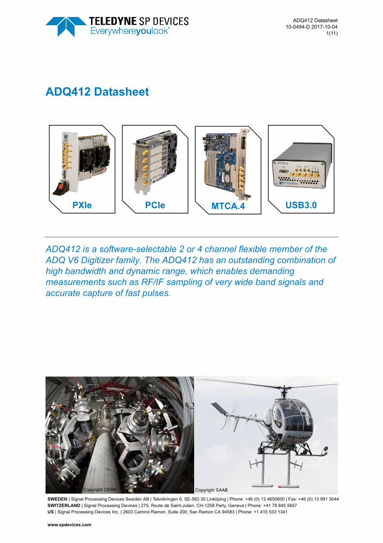
PXIe PCIe USB3.0MTCA.4
ADQ412 is a software-selectable 2 or 4 channel flexible member of the ADQ V6 Digitizer family. The ADQ412 has an outstanding combination of high bandwidth and dynamic range, which enables demanding measurements such as RF/IF sampling of very wide band signals and accurate capture of fast pulses.
Copyright SAABCopyright CERN
SWEDEN | Signal Processing Devices Sweden AB | Teknikringen 6, SE-583 30 Linköping | Phone: +46 (0) 13 4650600 | Fax: +46 (0) 13 991 3044
SWITZERLAND | Signal Processing Devices | 275, Route de Saint-Julien, CH-1258 Perly, Geneva | Phone: +41 78 845 5657
US | Signal Processing Devices Inc. | 2603 Camino Ramon, Suite 200, San Ramon CA 94583 | Phone: +1 415 533 1341
www.spdevices.com
ADQ412 Datasheet10-0494-D 2017-10-04
2(11)
ADQ412 Datasheet
Features Applications
• Up to 4 analog channels
• Up to 4 GSPS per channel sampling rate
• 12 bits resolution
• AC-coupling for high dynamic range
• Optional bias for unipolar pulse capture
• Up to 2 GHz analog bandwidth
• Internal and external clock reference
• Clock reference output
• External trigger input and output
• Multi record >1 MHz PRF
• Time stamp
• 700 Msamples data memory
• Data interface USB 3.0 / cPCIe / PXIe / PCIe / MTCA
• FPGA open for custom applications
ADQ412 Development Kit
• FPGA open for custom applications
• Real-time signal processing
• RADAR
• LIDAR
• Wireless communication
• Optical transmission
• High-speed data recording
• Test and measurement
• Ultrasonic ranging
• Pulse capture
Advantages
• Host PC interface options for optimized sys-tems partitioning.
• Sampling rate options for building family of products and streamlined maintenance. This optimizes cost of ownership.
• Real-time custom processing solutions for advanced systems.
• SP Devices’ design service is always avail-able for fast integration to reduce TTM.
Introduction
The ADQ412 is a flexible member in the ADQ V6 Digitizer family. It can be configured either as 2 or 4 analog input channels through a software con-trol. There are several sample rate options; 2, 3.6 or 4 GSPS per channel in 2-channel mode and 1, 1.8 or 2 GSPS per channel in 4-channel mode. The vertical resolution is 12 bits. The analog input bandwidth is up to 2 GHz and a total of 700 Msamples data memory. The ADQ412 is opti-mized for dynamic performance over a wide band-width, which makes it ideal for broadband applications such as IF/RF sampling and high-speed data recording.
The ADQ412 offers an easy-to-use API that allows for easy integration into any application. The software development kit (SDK) is included with the digitizer.
The ADQ412 digitizer is available in several form factors to meet different systems integrations requirements; USB3.0 for stand alone operation, cPCIe / PXIe / Micro-TCA.4 for modular instru-ments, and PCIe for integration in a PC.
ADQ412 Development Kit
The ADQ412 is equipped with an powerful Xilinx V6 LX240T FPGA which is partly available for customized real-time applications. SP Devices’ ADQ412 Development Kit is an optional FPGA programming tool that enables custom real-time signal processing of streaming data.
The ADQ412 Development Kit is purchased sepa-rately. More details about this product can be found in the datasheet for the ADQ Development Kit.
10-0494 D 2017-10-04 2(11)
ADQ412 Datasheet10-0494-D 2017-10-04
3(11)
1 Technical data1 Table 1:
KEY PARAMETERS OVERVIEW
Vertical resolution 12
Analog channels 2 / 4
Signal range 800 mVpp
Bias setting Factory installed
Sample rate Up to 4 GSPS, see below
Impedance AC 50
Analog bandwidth AC 6 kHz–2 GHz
Channel-to-channel skew 60 ps
Cross talk –80 dBc
Table 2:
SAMPLE RATE OPTIONS
OPTION –1G –3G –4G
4-CHANNEL MODE
Number of channels 4 4 4
Sampling rate 1 1.8 2 GSPS
Analog bandwidth 2 2 2 GHz
SFDR @149MHz 63 63 63 dBc
SNR @149MHz 57 57 55 dB
2-CHANNEL MODE
Number of channels 2 2 2
Sampling rate 2 3.6 4 GSPS
Analog bandwidth 1.3 1.3 1.3 GHz
SFDR @149MHz 60 60 63 dBc
SNR @149MHz 55 55 55 dB
Table 3:
GPIO
Number of GPIO 5
Output impedance pin #5 33
Output impedance Pin #1–4 100
Output (low – high) 0.1 – 3.2 V
Input impedance 10 k
Input (low – high) 1 – 2.3 V
Connector Micro DSUB 9 way
Table 4:
EXTERNAL CLOCK SOURCE
Frequency 4 channels mode FS MHz
Frequency 2 channels mode FS/2 MHz
Signal level (min – max) 0 – 10 dBm
0.64 – 2 Vpp
Impedance AC 50
Duty cycle 50%
Connector SMA
1. All values are typical unless otherwise noted.
Table 5:
CLOCK REFERENCE INPUT
Internal clock reference
Frequency 10 MHz
Accuracy 5 0.5/y ppm
External clock reference
Frequency (min – max) 1 – 250 MHz
Signal level (min – max) 0.8 – 3.3 VPP
Impedance AC 50
Duty cycle 50% ± 5%
Connector –USB, –PCIe, –PXIE
MCX
Connector –MTCA MMCX
PXIe clock reference1
PXIe clock 100 MHz
PXIe sync2 10 MHz
1. Available on PXIe form factor only2. Jitter reduced by PXIe clock in digitizer
Table 6:
CLOCK REFERENCE OUTPUT
Frequency Set by clock reference
Signal level 3.3 VPP
Impedance AC 50
Duty cycle 50% ± 5%
Connector –USB, –PCIe, –PXIE
MCX
Connector –MTCA MMCX
Table 7:
EXTERNAL TRIGGER INPUT
Input impedance DC 50
Input range (min – max) –0.4 to 2.4 V
Threshold rising/falling edge 500 mV
Sensitivity 200 mV
Jitter 25 ps
Resolution 1/FS s
Connector –USB, –PCIe, –PXIE
MCX
Connector –MTCA MMCX
Table 8:
TRIGGER OUTPUT
Output impedance 30
Output (low – high) 0.1 – 3.2 V
Connector –USB, –PCIe, –PXIE
MCX
Connector –MTCA MMCX
10-0494 D 2017-10-04 3(11)
ADQ412 Datasheet10-0494-D 2017-10-04
4(11)
2 Absolute maximum ratings
Exposure to conditions exceeding these ratings may reduce lifetime or permanently damage the device.
The ADQ412 has a built-in fan to cool the device. The built in temperature surveillance unit will pro-tect the ADQ412 from overheating by temporarily shutting down parts of the device in such a situa-tion.
The SMA connectors have an expected life time of 500 operations. For frequent connecting and dis-connecting of cables, connector savers are rec-ommended.
3 Dynamic performance
3.1 Noise and distortion
Table 9:
POWER SUPPLY
Supply Voltage 12 V
Power 43 W
Connector –USB External power supply1
Connector –PCIe 6-pin ATX power
Connector –PXIE from slot
Connector –MTCA from slot
1. Use only power supply included with the ADQ412.
Table 10:
ABSOLUTE MAXIMUM RATINGS
MIN MAX
Supply voltage (to GND) –0.4 V 14 V
Trigger input (to GND) –3 V 3.7 V
GPIO input (to GND)1
1. A voltage on a GPIO input higher than 3.3 V may change the output voltage on GPIOs which are set to outputs. This may damage external equipment.
–1 V 4.6 V
Clock ref (AC) 3.3 VPP
Ambient temperature (operation)
0 oC 45 oC
Analog inputs
AC > 1kHz 5 Vpp
DC –2.5 V 2.5 V
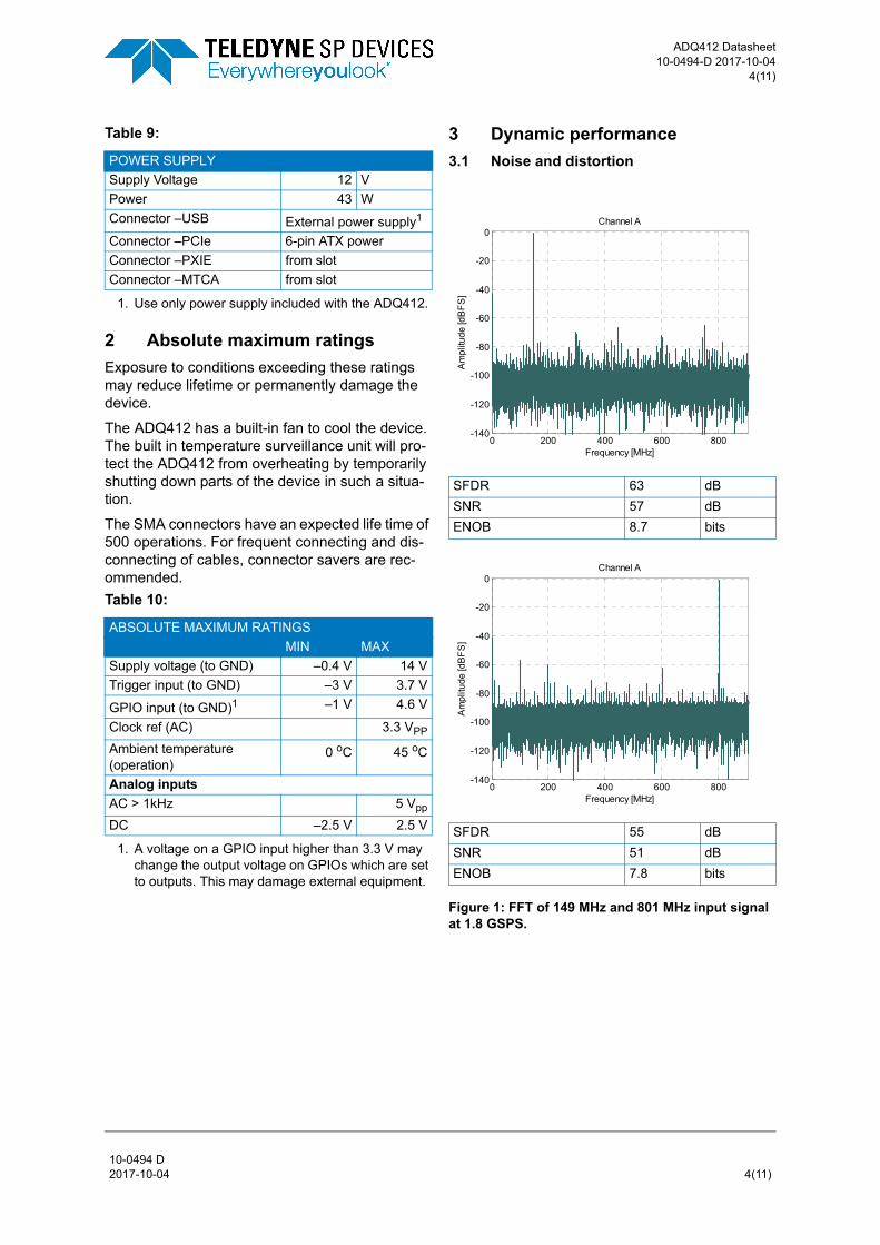
SFDR 63 dB
SNR 57 dB
ENOB 8.7 bits
SFDR 55 dB
SNR 51 dB
ENOB 7.8 bits
Figure 1: FFT of 149 MHz and 801 MHz input signal at 1.8 GSPS.
0 200 400 600 800-140
-120
-100
-80
-60
-40
-20
0
Frequency [MHz]A
mp
litu
de
[dB
FS
]
Channel A
0 200 400 600 800-140
-120
-100
-80
-60
-40
-20
0
Frequency [MHz]
Am
plit
ud
e [d
BF
S]
Channel A
10-0494 D 2017-10-04 4(11)

ADQ412 Datasheet10-0494-D 2017-10-04
5(11)
4 Functional overview
4.1 Block diagram
The digitizer includes an analog front-end with sig-nal conditioning and A/D conversions and a digital back-end for data flow control, triggering, and host communication.
4.2 Analog front-end
The ADQ412 can operate in a 4-channel mode where each ADC is connected to one analog input channel, Figure 2. In the 2-channel mode, two ADCs operate on the same analog input in an interleaved mode, Figure 3. This doubles the sampling rate. The interleaving is enabled by ADX, see Section 4.3. Switching between 2- and 4-channel mode is done in software.
The analog front-end contains AC-coupling and an optional DC-bias. The bias is set in factory and enables unipolar pulse capture, Section 4.4.
4.3 Interleaving ADX
The high data rate in 2-channel mode is enabled by SP Devices’ proprietary technology for inter-leaving of ADCs: ADX.
4.4 Biased AC-coupled front-end
For unipolar signals, a biased front-end is avail-able. It places the zero level at a pre-biased level and the entire input signal range can therefor be used to measure the pulses.
A positive bias (for negative pulses) is available at 90% of the signal range.
Order code: –PB
A negative bias (for positive pulses) is available at 10% of the signal range.
Order code: –NB
Figure 2: Block diagram 4-channel mode. Figure 3: Block diagram 2-channel mode.
������
����
���
����� � � ��!�
�� �
���
"�
� �
�
���
���
���
��
#!�
� �
��!
�
$����!����
�� ���!����
$����!�� %
����& !�����
�� ���!�� %
�� ����
��
#!�'��
(#!
�'�
��
#!��� !
���!
��#)
*+!
���
��
��
�����
�
�
,��+� � �
�� ����!��-�(#!.
��
�
����
�!
�!
�
$�()
*/
,�
� �
��!
�
*/
,0�1
���
!��
�!
������
����
���
����� � � ��!�
�� �
���
"�
� �
�
���
���
���
�����!����
�� ���!����
�����!�� �
����� !�����
�� ���!�� �
�� ����
����
��!
���
��
�����
�� � �
���� � �
�� ����!�����!�
��
�
����
�!
�!
�
����
��
��
�� ��
�!�
� �
��!
�
��
�!�
���
�!�
��
��!
���
!��
�!
�/
�
� �
��!
�
�/
0�1
���
!��
�!
Figure 4: Bias option.
–PB at 90%
–NB at 10%
10-0494 D 2017-10-04 5(11)
ADQ412 Datasheet10-0494-D 2017-10-04
6(11)
4.5 Data recording
There are several methods for data recording to serve different use cases;
• Multi-record recording in on-board DRAM for very long records.
• Triggered streaming for fast data transfer and long measurement time.
• Individual level trigger for multi-channel pulse capture
• Continuous multi-record via on-board DRAM for acquisition of long records during long
measurement time.1
• Continuous streaming of data to the host PC
for real time analysis of data2
To support data recording, there is on board DRAM of 1 GBytes. The interface to the host PC enables up to 3.2 GBytes/s over a Gen2 x8 PCIe interface.
4.6 Signal processing
There is support for real-time signal processing on the digitizer;
• Real-time waveform averaging.
• Level trigger for event detection.
• Gain and offset calibration.
• Custom real-time signal processing can be implemented using the ADQ412 Development Kit.
4.7 Trigger
There are several trigger modes;
• External for synchronization.
• Level trigger for data driven acquisition.
• Software for user’s control.
• Internal for automatic sequencing.
There is also a trigger output for triggering exter-nal equipment. The trigger timing is controlled by pre-trigger buffer and trigger delay parameter set-tings.
4.8 Clock
There are several modes for clocking the digitizer
• Internal clock for stand alone operation
• External clock for synchronization
• External clock reference for synchronization
There is also a clock reference output for clocking external equipment.
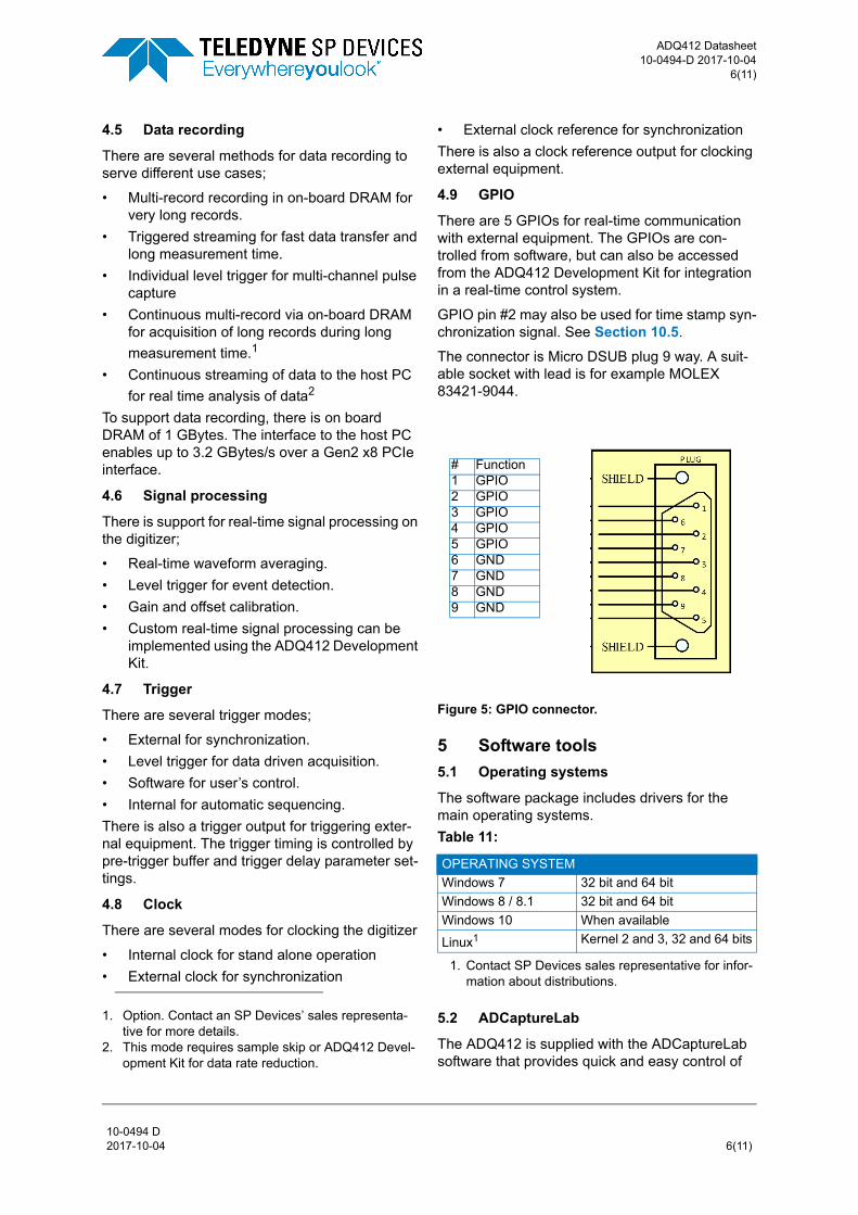
4.9 GPIO
There are 5 GPIOs for real-time communication with external equipment. The GPIOs are con-trolled from software, but can also be accessed from the ADQ412 Development Kit for integration in a real-time control system.
GPIO pin #2 may also be used for time stamp syn-chronization signal. See Section 10.5.
The connector is Micro DSUB plug 9 way. A suit-able socket with lead is for example MOLEX 83421-9044.
5 Software tools
5.1 Operating systems
The software package includes drivers for the main operating systems.
5.2 ADCaptureLab
The ADQ412 is supplied with the ADCaptureLab software that provides quick and easy control of
1. Option. Contact an SP Devices’ sales representa-tive for more details.
2. This mode requires sample skip or ADQ412 Devel-opment Kit for data rate reduction.
# Function1 GPIO2 GPIO3 GPIO4 GPIO5 GPIO6 GND7 GND8 GND9 GND
Figure 5: GPIO connector.
Table 11:
OPERATING SYSTEM
Windows 7 32 bit and 64 bit
Windows 8 / 8.1 32 bit and 64 bit
Windows 10 When available
Linux1
1. Contact SP Devices sales representative for infor-mation about distributions.
Kernel 2 and 3, 32 and 64 bits
10-0494 D 2017-10-04 6(11)
ADQ412 Datasheet10-0494-D 2017-10-04
7(11)
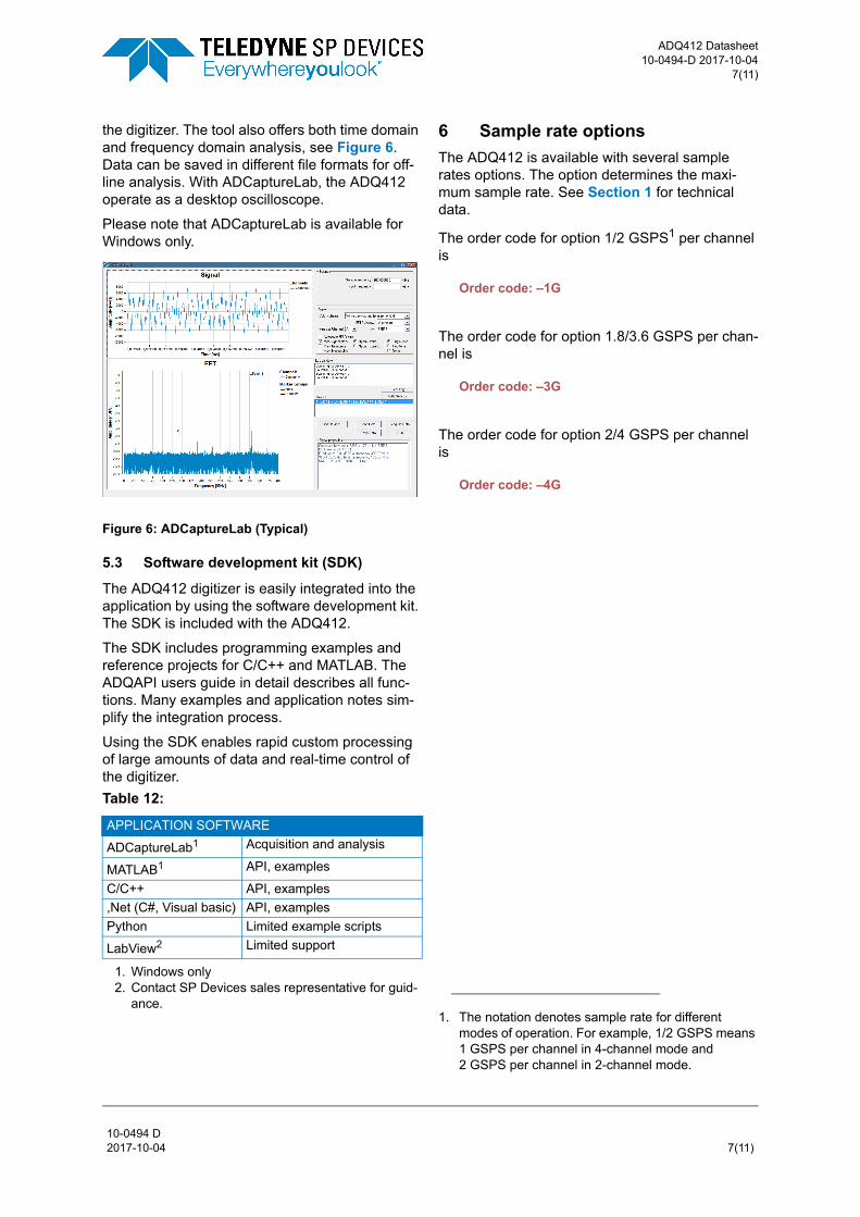
the digitizer. The tool also offers both time domain and frequency domain analysis, see Figure 6. Data can be saved in different file formats for off-line analysis. With ADCaptureLab, the ADQ412 operate as a desktop oscilloscope.
Please note that ADCaptureLab is available for Windows only.
5.3 Software development kit (SDK)
The ADQ412 digitizer is easily integrated into the application by using the software development kit. The SDK is included with the ADQ412.
The SDK includes programming examples and reference projects for C/C++ and MATLAB. The ADQAPI users guide in detail describes all func-tions. Many examples and application notes sim-plify the integration process.
Using the SDK enables rapid custom processing of large amounts of data and real-time control of the digitizer.
6 Sample rate options
The ADQ412 is available with several sample rates options. The option determines the maxi-mum sample rate. See Section 1 for technical data.
The order code for option 1/2 GSPS1 per channel is
Order code: –1G
The order code for option 1.8/3.6 GSPS per chan-nel is
Order code: –3G
The order code for option 2/4 GSPS per channel is
Order code: –4G
Figure 6: ADCaptureLab (Typical)
Table 12:
APPLICATION SOFTWARE
ADCaptureLab1
1. Windows only
Acquisition and analysis
MATLAB1 API, examples
C/C++ API, examples
,Net (C#, Visual basic) API, examples
Python Limited example scripts
LabView2
2. Contact SP Devices sales representative for guid-ance.
Limited support
1. The notation denotes sample rate for different modes of operation. For example, 1/2 GSPS means 1 GSPS per channel in 4-channel mode and 2 GSPS per channel in 2-channel mode.
10-0494 D 2017-10-04 7(11)
ADQ412 Datasheet10-0494-D 2017-10-04
8(11)
7 Digital interface options
The ADQ V6 digitizer family supports various number of interfaces. The digital interface is used for control and data transfer between the host and the digitizer.
7.1 Firmware upgrade interface
Regardless of the selected data interface, there is always an additional USB interface for firmware upgrade. This connection is not related to the data and control interface.
7.2 USB interface
With the SuperSpeed USB interface, the digitizer is easily connected to any computer.
Order code: –USB
7.3 cPCIe / PXIe interface
The ADQ412 is available with cPCIe / PXIe inter-face.
Order code: –PXIE
Table 13:
USB INTERFACE
Standard USB 3.0
Data rate sustained 200 MB/s
Box size 53 x 106 x 166
mm3
(a) Front panel
(b) Rear panel
Figure 7: ADQ412 with USB3.0 interface.
Table 14:
cPCIe / PXIe INTERFACE
Bus width 8 lanes
Bus peak capacity 16 Gbit/s
Sustained data rate, 8 lanes1
1. This is depending performance of the system including the controller, chassis and application software.
3.2 GByte/s
PXIe card size 3U 2 slot 8TE
Figure 8: cPCIe / PXIe card.
10-0494 D 2017-10-04 8(11)
ADQ412 Datasheet10-0494-D 2017-10-04
9(11)
7.4 PCIe interface
The ADQ412 is available with PCIe Gen2 x8 inter-face.
Order code: –PCIe
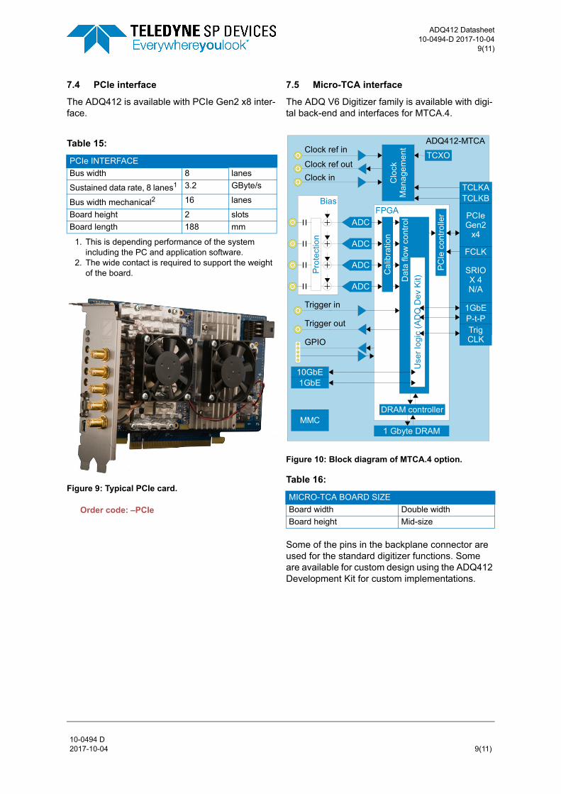
7.5 Micro-TCA interface
The ADQ V6 Digitizer family is available with digi-tal back-end and interfaces for MTCA.4.
Some of the pins in the backplane connector are used for the standard digitizer functions. Some are available for custom design using the ADQ412 Development Kit for custom implementations.
Table 15:
PCIe INTERFACE
Bus width 8 lanes
Sustained data rate, 8 lanes1
1. This is depending performance of the system including the PC and application software.
3.2 GByte/s
Bus width mechanical2
2. The wide contact is required to support the weight of the board.
16 lanes
Board height 2 slots
Board length 188 mm
Figure 9: Typical PCIe card.
Figure 10: Block diagram of MTCA.4 option.
Table 16:
MICRO-TCA BOARD SIZE
Board width Double width
Board height Mid-size
�����������
!"#�
���
�$��%��&'����(��
�'�
% ����������
��
��
��
�� ������� �
����� ����
����� ����
����� ���%�
����&� �����
����� ���%�
������
����
�� ��������
��
��� ���������������
���
����� � ��
� �
�!�"
�!��
#!�
�� � ��$�
2��� ��34�
�%�%�
���5
����!�
"���
���� �����
�6��5
���5
��
10-0494 D 2017-10-04 9(11)
ADQ412 Datasheet10-0494-D 2017-10-04
10(11)
Order code: –MTCA
Ordering information
Table 17:
MICRO-TCA INTERFACE
Signal Port Status
1GbE 0 ADQ412 Dev Kit
PCIe 4-7 Standard
Point-to-point 12-15 ADQ412 Dev Kit
Trigger, Data, Clocks 17-20 ADQ412 Dev Kit
TCLKA Clk 1 Standard
TCLKB Clk 2 Standard
FCLKA Clk 3 Standard
Table 18:
FRONT PANEL ADDITIONAL INTERFACE
Signal Connector Status
1 GbE SFP ADQ412 Dev Kit
10 GbE SFP+ ADQ412 Dev Kit
LED Red (Error) LED Green (Operating OK)
10 GbE SFP+
1 GbE SFP
GPIO Micro D 9-w plug
Ext Clock SMA USB 2.0 Mini-B
Trig out MMCXChannel A SMA
Trig in MMCX
Channel B SMA Clk ref out MMCX
Clk ref in MMCXChannel C SMA
LED Yellow (Ready)Channel D SMA
LED Red/Green (Power/Status)
LED Blue (hot swap)Handle
Figure 11: Front panel of ADQ412–MTCA.
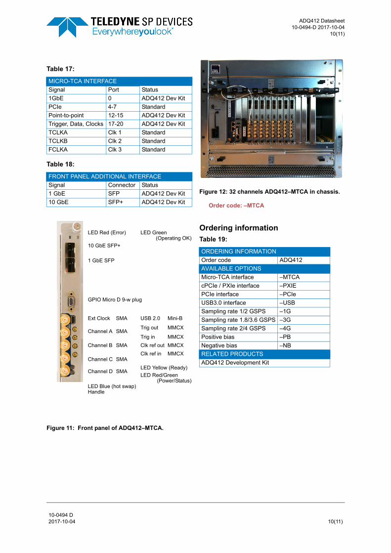
Figure 12: 32 channels ADQ412–MTCA in chassis.
Table 19:
ORDERING INFORMATION
Order code ADQ412
AVAILABLE OPTIONS
Micro-TCA interface –MTCA
cPCIe / PXIe interface –PXIE
PCIe interface –PCIe
USB3.0 interface –USB
Sampling rate 1/2 GSPS –1G
Sampling rate 1.8/3.6 GSPS –3G
Sampling rate 2/4 GSPS –4G
Positive bias –PB
Negative bias –NB
RELATED PRODUCTS
ADQ412 Development Kit
10-0494 D 2017-10-04 10(11)

SWEDEN | Signal Processing Devices Sweden AB | Teknikringen 6, SE-583 30 Linköping | Phone: +46 (0) 13 4650600 | Fax: +46 (0) 13 991 3044
SWITZERLAND | Signal Processing Devices | 275, Route de Saint-Julien, CH-1258 Perly, Geneva | Phone: +41 78 845 5657
US | Signal Processing Devices Inc. | 2603 Camino Ramon, Suite 200, San Ramon CA 94583 | Phone: +1 415 533 1341
www.spdevices.com
ADQ412 Datasheet10-0494-D 2017-10-04
11(11)
Important Information
Teledyne Signal Processing Devices Sweden AB (Teledyne SP Devices) reserve the right to make cor-rections, modifications, enhancements, improvements, and other changes to its products and services at any time and to discontinue any product or service without notice. Customers should obtain the latest relevant information before placing orders and should verify that such information is current and com-plete. All products are sold subject to Teledyne SP Devices’ general terms and conditions supplied at the time of order acknowledgment.
Teledyne SP Devices warrants that each product will be free of defects in materials and workmanship, and conform to specifications set forth in published data sheets, for a period of one (1) year. The war-ranty commences on the date the product is shipped by Teledyne SP Devices. Teledyne SP Devices’ sole liability and responsibility under this warranty is to repair or replace any product which is returned to it by Buyer and which Teledyne SP Devices determines does not conform to the warranty. Product returned to Teledyne SP Devices for warranty service will be shipped to Teledyne SP Devices at Buyer’s expense and will be returned to Buyer at Teledyne SP Devices’ expense. Teledyne SP Devices will have no obligation under this warranty for any products which (i) has been improperly installed; (ii) has been used other than as recommended in Teledyne SP Devices’ installation or operation instruc-tions or specifications; or (iii) has been repaired, altered or modified by entities other than Teledyne SP Devices. The warranty of replacement products shall terminate with the warranty of the product. Buyer shall not return any products for any reason without the prior written authorization of Teledyne SP Devices.
In no event shall Teledyne SP Devices be liable for any damages arising out of or related to this docu-ment or the information contained in it.
TELEDYNE SP DEVICES’ EXPRESS WARRANTY TO BUYER CONSTITUTES TELEDYNE SP DEVICES’ SOLE LIABILITY AND THE BUYER’S SOLE REMEDY WITH RESPECT TO THE PROD-UCTS AND IS IN LIEU OF ALL OTHER WARRANTIES, LIABILITIES AND REMEDIES. EXCEPT AS THUS PROVIDED, TELEDYNE SP DEVICES DISCLAIMS ALL WARRANTIES, EXPRESS OR IMPLIED, INCLUDING ANY WARRANTY OF MERCHANTABILITY, FITNESS FOR A PARTICULAR PURPOSE OR NON-INFRINGEMENT.
TELEDYNE SP DEVICES DOES NOT INDEMNIFY, NOR HOLD THE BUYER HARMLESS, AGAINST ANY LIABILITIES, LOSSES, DAMAGES AND EXPENSES (INCLUDING ATTORNEY’S FEES) RELAT-ING TO ANY CLAIMS WHATSOEVER. IN NO EVENT SHALL TELEDYNE SP DEVICES BE LIABLE FOR SPECIAL, INCIDENTAL OR CONSEQUENTIAL DAMAGES, INCLUDING LOST PROFIT, LOST DATA AND THE LIKE, DUE TO ANY CAUSE WHATSOEVER. NO SUIT OR ACTION SHALL BE BROUGHT AGAINST TELEDYNE SP DEVICES MORE THAN ONE YEAR AFTER THE RELATED CAUSE OF ACTION HAS ACCRUED. IN NO EVENT SHALL THE ACCRUED TOTAL LIABILITY OF TELEDYNE SP DEVICES FROM ANY LAWSUIT, CLAIM, WARRANTY OR INDEMNITY EXCEED THE AGGREGATE SUM PAID TO SP BY BUYER UNDER THE ORDER THAT GIVES RISE TO SUCH LAWSUIT, CLAIM, WARRANTY OR INDEMNITY.
Worldwide Sales and Technical Support
www.spdevices.com
Teledyne SP Devices Corporate Headquarters
Teknikringen 6SE-583 30 LinköpingSweden
Phone: +46 (0)13 465 0600Fax: +46 (0)13 991 3044Email: [email protected]
Copyright © 2017 Teledyne Signal Processing Devices Sweden AB. All rights reserved, including those to repro-duce this publication or parts thereof in any form without permission in writing from Teledyne SP Devices.