1 ece734 vlsi arrays for digital signal processing chapter 4 retiming
TRANSCRIPT

1ECE734 VLSI Arrays for Digital Signal Processing
Chapter 4 Retiming
(C) 2004-2006 by Yu Hen Hu 2ECE734 VLSI Arrays for Digital Signal Processing
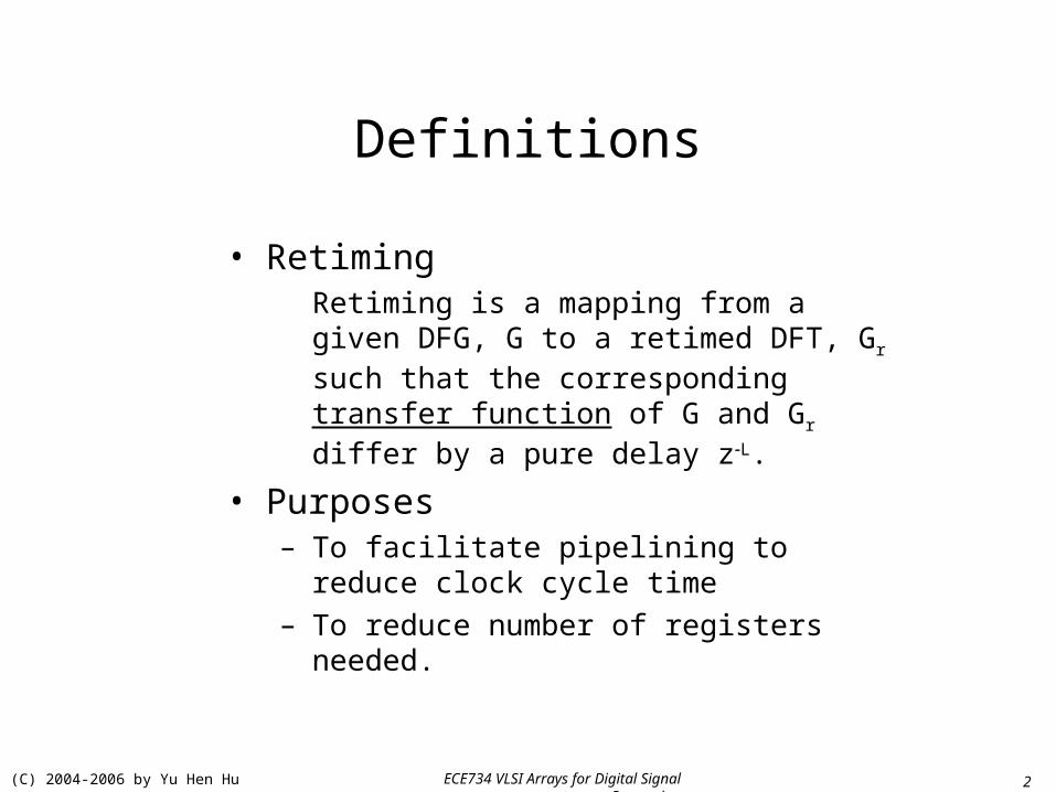
Definitions
• RetimingRetiming is a mapping from a given DFG, G to a retimed DFT, Gr such that the corresponding transfer function of G and Gr differ by a pure delay zL.
• Purposes– To facilitate pipelining to reduce clock cycle
time– To reduce number of registers needed.

(C) 2004-2006 by Yu Hen Hu 3ECE734 VLSI Arrays for Digital Signal Processing
Cut-set Retiming
• Feed-forward cut-set:
• Feed-back cut-set
• Delay transfer theorem– Adding arbitrary non-
negative number of delays to each edge of a feed-forward cut-set of a DFG will not alter its output, except the output timing will be delayed.
– Transfer the same amount of delays from edges of the same direction across a feed-back cut set of a DFG to all edges of opposing edges across the same cut set will not alter the output, but its timing.

(C) 2004-2006 by Yu Hen Hu 4ECE734 VLSI Arrays for Digital Signal Processing
Feed-forward Cut-Set Retiming
• Consider the FIR digital filter and its DFG:
y(n) = b0x(n) + b1x(n1)
• Critical path length = TM+TA
• Select a cut set • Insert a delay each to each
edge in the cut set.
• Retiming:
ynew(n) = b0x(n) + b1x(n2)
ynew(n) = y(n
• Critical path = Max(TM, TA)
X X
+
Dx(n) x(n1)
y(n)
b1b0
X X
+
Dx(n) x(n1)
y(n)
b1b0
DD

(C) 2004-2006 by Yu Hen Hu 5ECE734 VLSI Arrays for Digital Signal Processing
Feed-back Cut Set Retiming
• Consider an IIR digital filter
y(n) = a·y(n-2) + x(n)
loop bound = (TM+TA)/2
clock cycle = TM+TA
• Shift 1 delay to the other edge across a feed-back cut set
• Filter remains unchanged.
loop bound = (TM+TA)/2
clock cycle = Max(TM ,TA)
+
2D
x(n) y(n)
a
+
D
x(n) y(n)
a
D
(C) 2004-2006 by Yu Hen Hu 6ECE734 VLSI Arrays for Digital Signal Processing
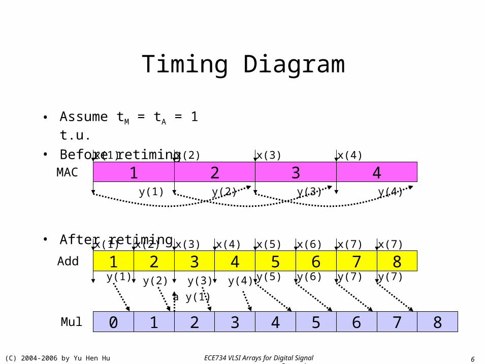
Timing Diagram
• Assume tM = tA = 1 t.u.
• Before retiming
• After retiming
1 2 3 4x(1) x(2) x(3) x(4)
y(1) y(2) y(3) y(4)
1 2 3 4 5 6 7 8x(1) x(2) x(3) x(4) x(5) x(6) x(7) x(7)
MAC
1 2 3 4 5 6 7 8
y(1) y(2) y(3) y(4) y(5) y(6) y(7) y(7)Add
a y(1)
Mul 0

(C) 2004-2006 by Yu Hen Hu 7ECE734 VLSI Arrays for Digital Signal Processing
Feed-back Cut Set Retiming
• Consider an IIR digital filter
y(n) = ay(n-1) + x(n)
loop bound = (TM+TA)
throughput = 1/(TM+TA)
+
D
x(n) y(n)
a
x(2k-1)=x(k)
x(2k) = 0
Clock period = (TM+TA)
Throughput = 1/[2(TM+TA)]
+
2D
x(m) y(m)
a

(C) 2004-2006 by Yu Hen Hu 8ECE734 VLSI Arrays for Digital Signal Processing
Slowdown + Retiming
Start with
y(n) = a y(n-1) + x(n)
clock cycle = Max(TM ,TA)
Throughput = 1/[2max(TM,TA)]
Start with y(n) = a y(n-2) + x(n)
loop bound = (TM+TA)/2
clock cycle = Max(TM ,TA)
throughput = 1/ Max(TM ,TA)
+
D
x(m) y(m)
a
D
+
D
x(n) y(n)
a
D
(C) 2004-2006 by Yu Hen Hu 9ECE734 VLSI Arrays for Digital Signal Processing
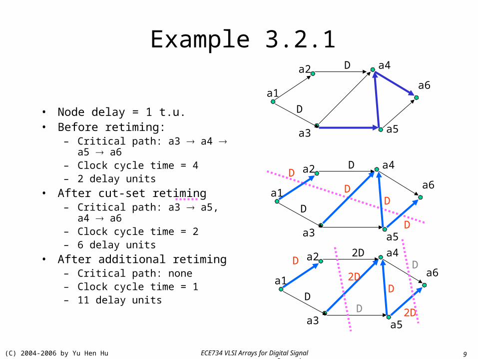
Example 3.2.1
• Node delay = 1 t.u.• Before retiming:
– Critical path: a3 a4 a5 a6
– Clock cycle time = 4– 2 delay units
• After cut-set retiming – Critical path: a3 a5, a4 a6– Clock cycle time = 2– 6 delay units
• After additional retiming– Critical path: none– Clock cycle time = 1– 11 delay units
D
D
a1
a2
a3
a4
a5
a6
D
D
a1
a2
a3
a4
a5
a6D
DD
D
2D
D
a1
a2
a3
a4
a5
a6D
2DD
2DD
D
(C) 2004-2006 by Yu Hen Hu 10ECE734 VLSI Arrays for Digital Signal Processing
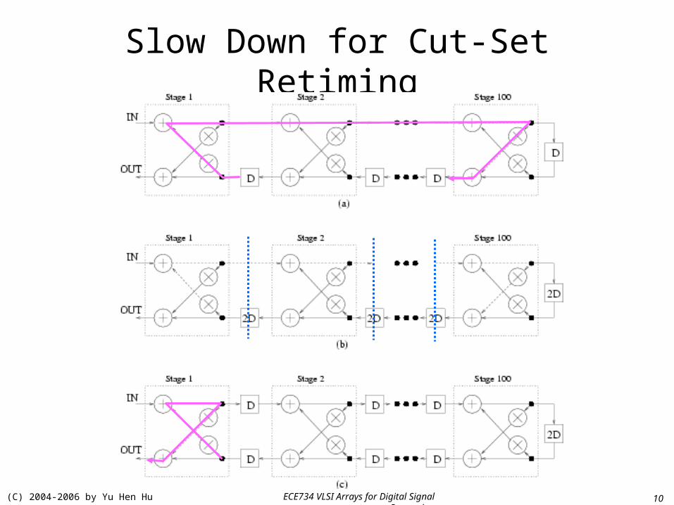
Slow Down for Cut-Set Retiming

(C) 2004-2006 by Yu Hen Hu 11ECE734 VLSI Arrays for Digital Signal Processing
Node Retiming
• Transfer delay through a node in DFG:
• r(v) = # of delays transferred from out-going edges to incoming edges of node v w(e) = # of delays on edge e
• wr(e) = # of delays on edge e after retiming
• Retiming equation:
subject to wr(e) 0.
• Let p be a path from v0 to vk
then
v v
3D
D2D
3D
D2D
r(v) = 2 ( ) ( ) ( ) ( )rw e w e r v r u
1
0
1
10
0
( ) ( )
( ) ( ) ( )
( ) ( ) ( )
k
r r ii
k
i i ii
k
w p w e
w e r v r v
w p r v r v
v0e0 v1
e1 … vkek
u ve
p

(C) 2004-2006 by Yu Hen Hu 12ECE734 VLSI Arrays for Digital Signal Processing
Invariant Properties
1. Retiming does NOT change the total number of delays for each cycle.
2. Retiming does not change loop bound or iteration bound of the DFG
3. If the retiming values of every node v in a DFG G are added to a constant integer j, the retimed graph Gr will not be affected. That is, the weights (# of delays) of the retimed graph will remain the same.
(C) 2004-2006 by Yu Hen Hu 13ECE734 VLSI Arrays for Digital Signal Processing
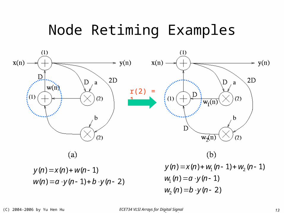
Node Retiming Examples
r(2) = 1
1 2
1
2
( ) ( ) ( 1) ( 1)
( ) ( 1)
( ) ( 2)
y n x n w n w n
w n a y n
w n b y n
( ) ( ) ( 1)
( ) ( 1) ( 2)
y n x n w n
w n a y n b y n

(C) 2004-2006 by Yu Hen Hu 14ECE734 VLSI Arrays for Digital Signal Processing
DFG Illustration of the Example
T = max. {(1+2+1)/2, (1+2+1)/3} = 2Cr. Path delay = 2+1 = 3 t.u
T = max. {(1+2+1)/2, (1+2+1)/3} = 2Cr. Path Delay = max{2,2,1+1} = 2 t.u

(C) 2004-2006 by Yu Hen Hu 15ECE734 VLSI Arrays for Digital Signal Processing
Retiming for Minimizing Clock Period
• Note that retiming will NOT alter iteration bound T.
• Iteration bound is the theoretical minimum clock period to execute the algorithm.
• Let edge e connect node u to node v. If the node computing time t(u) + t(v) > T, then clock period T > T. For such an edge, we require that
• To generalize, for any path from v0 to vk, we have
• In other words, for any possible critical path in the DFG that is larger than T, we require wr(e) 1.
0( ) ( ) ( ) ( )r kw p w p r v r v
0
( ) ( ) ,
( ) 1
k
ii
r
t p t v T
w p
If
then we require .
( ) 1rw e

(C) 2004-2006 by Yu Hen Hu 16ECE734 VLSI Arrays for Digital Signal Processing
Retiming Example Revisited
wr(e21) 0, since t(2)+t(1) = 2 = T.
wr(e13) 1, since t(1)+t(3) = 3 > T.
wr(e14) 1, since t(1)+t(4) = 3 > T.
wr(e32) 1, since t(3)+t(2) = 3 > T.
wr(e42) 1, since t(4)+t(2) = 3 > T.
Use eq. wr(euv) = w(e) + r(v) – r(u),
w(e21) + r(1) – r(2) = 1 + r(1) – r(2) 0
w(e13) + r(3) – r(1) = 1 + r(3) – r(1) 1
w(e14) + r(4) – r(1) = 2 + r(4) – r(1) 1
w(e32) + r(2) – r(3) = 0 + r(2) – r(3) 1
w(e42) + r(2) – r(4) = 0 + r(2) – r(4) 1
2T

(C) 2004-2006 by Yu Hen Hu 17ECE734 VLSI Arrays for Digital Signal Processing
Solution continues
• Since the retimed graph Gr remain the same if all node retiming values are added by the same constant. We thus can set r(1) = 0.
• The inequalities become
1 – r(2) 0 or r(2) 1
1 + r(3) 1 or r(3) 0
2 + r(4) 1 or r(4) –1
r(2) – r(3) 1 or r(3) r(2) 1r(2) – r(4) 1 or r(2) r(4) 1
• Since
one must have r(2) = 1. • This implies r(3) 0. But we
also have r(3) 0. Hence r(3)=0.
• These leave –1 r(4) 0. • Hence the two sets of
solutions are:
r(0) = r(3) = 0, r(2) = 1, and r(4) = 0 or 1.
1 (2) (3) 1 0 1 1r r

(C) 2004-2006 by Yu Hen Hu 18ECE734 VLSI Arrays for Digital Signal Processing
Systematic Solutions
Given a systems of inequalities:
r(i) – r(j) k; 1 i,j N
Construct a constraint graph:1. Map each r(i) to node i. Add
a node N+1.
2. For each inequality
r(i) – r(j) k,
draw an edge eji
such that w(eji) = k.
1. Draw N edges eN+1,i = 0.
a) The system of inequalities has a solution if and only if the constraint graph contains no negative cycles
b) If a solution exists, one solution is where ri is the minimum length path from the node N+1 to the node i.
Shortest path algorithms: (Applendix A)Bellman-Ford algorithmFloyd-Warshall algorithm

(C) 2004-2006 by Yu Hen Hu 19ECE734 VLSI Arrays for Digital Signal Processing
Bellman-Ford AlgorithmFind shortest path from an
arbitrarily chosen origin node U to each node in a directed graphif no negative cycle exists.
Given a direct graphw(m,n): weight on edge from node m to node n, = if there is no edge from m to n
r(i,j): the shortest path from node U to node i within j-1 steps. r(i,1) = w(U,i), r(i,j+1) = min {r(k,j) + w(k,i)},
j = 1, 2, …, N-1if max(r(:,n-1)-r(:,n))>0, then there is a negative cycle. Else, r(i,n-1) gives shortest cycle length from i to U.
Note that 1 > 0, hence there is at least one negative cycle.
21
34
11
2
3
1
0 3 2 2 2
0 1 1 0 0 1 1
0 2 1 1 1 0
1 0 1 1 1 0
W r
spbf.m

(C) 2004-2006 by Yu Hen Hu 20ECE734 VLSI Arrays for Digital Signal Processing
Floyd-Warshall Algorithm
Find shortest path between all possible pairs of nodes in the graph provided no negative cycle exists.
Algorithm:
Initialization: R(1) =W;
For k=1 to NR(k+1)(u,v) = min{R(k)(u,:) + R(k)
(:,v)}
If R(k)(u,u) < 0 for any k, u, then a negative cycle exist. Else, R(N+1)(u,v) is SP from u to v
21
34
21
2
3
1
(2)
(3) (4) (5)
0 3 0 3 2 1
0 1 2 3 0 1 2
0 2 3 0 2
1 0 1 2 0
0 3 2 1
3 0 1 2
3 0 0 2
1 2 1 0
W R
R R R
(C) 2004-2006 by Yu Hen Hu 21ECE734 VLSI Arrays for Digital Signal Processing
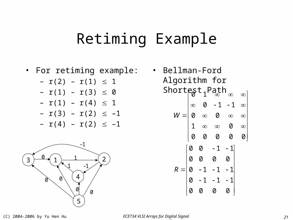
Retiming Example
• For retiming example: – r(2) – r(1) 1
– r(1) – r(3) 0
– r(1) – r(4) 1
– r(3) – r(2) –1
– r(4) – r(2) –1
• Bellman-Ford Algorithm for Shortest Path
213
4
5
1
1
00
00
0
1
1
0 1
0 1 1
0 0
1 0
0 0 0 0 0
0 0 1 1
0 0 0 0
0 1 1 1
0 1 1 1
0 0 0 0
W
R
(C) 2004-2006 by Yu Hen Hu 22ECE734 VLSI Arrays for Digital Signal Processing
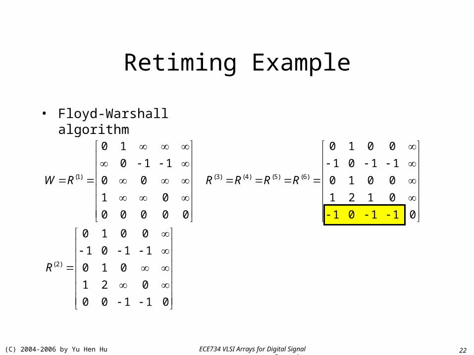
Retiming Example
• Floyd-Warshall algorithm
(1) (3) (4) (5) (6)
(2)
0 1 0 1 0 0
0 1 1 1 0 1 1
0 0 0 1 0 0
1 0 1 2 1 0
0 0 0 0 0 1 0 1 1 0
0 1 0 0
1 0 1 1
0 1 0
1 2 0
0 0 1 1 0
W R R R R R
R

(C) 2004-2006 by Yu Hen Hu 23ECE734 VLSI Arrays for Digital Signal Processing
Retiming to Reduce Registers
• Register SharingWhen a node has multiple fan-out with different number of delays, the registers can be shared so that only the branch with max. # of delays will be needed.
• Register reduction through node delay transfer from multiple input edges to output edges (e.g. r(v) > 0)
• Should be done only when clock cycle constraint (if any) is not violated.
D
D
D
Delay reduction

(C) 2004-2006 by Yu Hen Hu 24ECE734 VLSI Arrays for Digital Signal Processing
Time Scaling (Slow Down)
• Transform each delay element (register) D to ND and reduce the sample frequency by N fold will slow down the computation N times.
• During slow down, the processor clock cycle time remains unchanged. Only the sampling cycle time increased.
• Provides opportunity for retiming, and interleaving.
+
D
… x(3) x(2) x(1)
+
2D
… y(3) y(2) y(1)
… -- x(3) -- x(2) -- x(1) … y(3) -- y(2) -- y(1)