-1- thesis defense - andrew farris may 23, 2008 thesis defense – electrical engineering drop...
Post on 21-Dec-2015
217 views
TRANSCRIPT
-1-Thesis Defense - Andrew FarrisMay 23, 2008
Thesis Defense – Electrical Engineering
Drop Impact Reliability Testing
Lead-Free Chip Scale Packages
Andrew Farris
May 23, 2008
California Polytechnic State University
San Luis Obispo, CA 93407
-2-Thesis Defense - Andrew FarrisMay 23, 2008
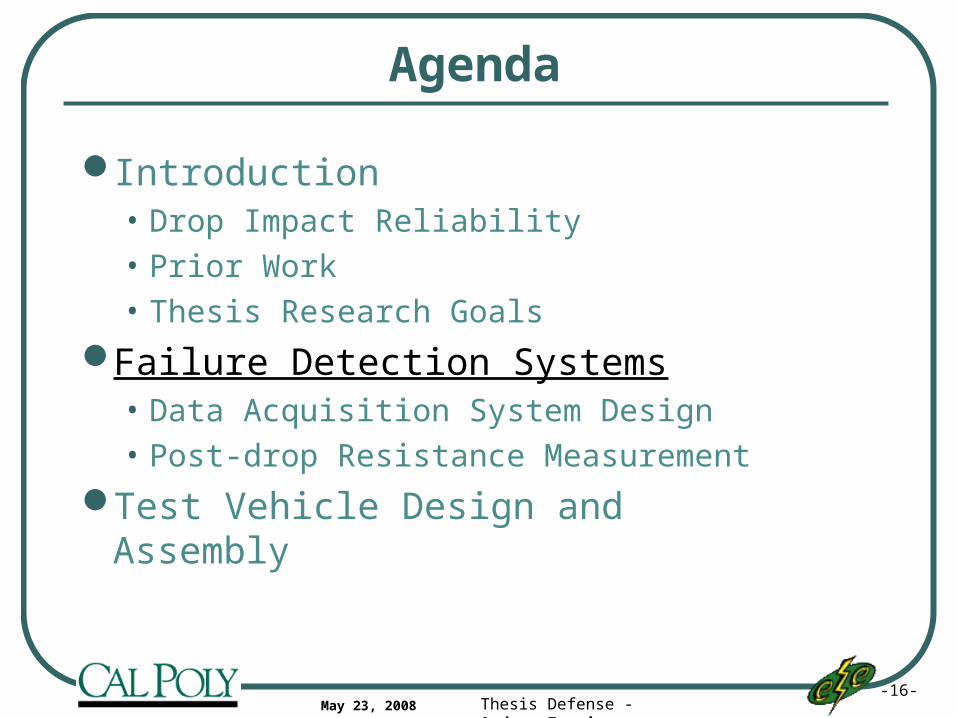
Agenda
Introduction• Drop Impact Reliability
• Prior Work
• Thesis Research Goals
Failure Detection Systems• Data Acquisition System Design
• Post-drop Resistance Measurement
Test Vehicle Design and Assembly
-3-Thesis Defense - Andrew FarrisMay 23, 2008
Agenda
Drop Impact TestingAnalysis
• Reliability Data
• Failure Mechanisms
• Acceleration on Test Vehicle
ConclusionsAcknowledgements
-4-Thesis Defense - Andrew FarrisMay 23, 2008
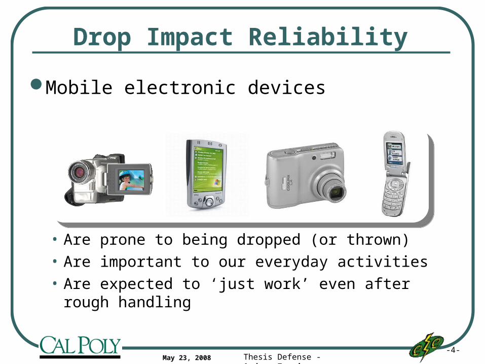
Drop Impact Reliability
Mobile electronic devices
• Are prone to being dropped (or thrown)
• Are important to our everyday activities
• Are expected to ‘just work’ even after rough handling
-5-Thesis Defense - Andrew FarrisMay 23, 2008
Drop Test Reliability (cont.)
Mobile electronic devices also…• Are complicated and expensive
• Are easily damaged by drop impacts
• Are designed to be lightweight and portable
Drop test reliability is:• The study of how well a device or part survives
repeated drop impacts
• A process to determine where design improvements are needed for future high reliability designs
-6-Thesis Defense - Andrew FarrisMay 23, 2008
Introduction to Drop Testing
What happens during a drop impact test• The electronics test vehicle is attached to a shock
test table
• The table is dropped vertically until it impacts a stationary base
• The impact causes an acceleration pulse by rapidly stopping the table (and test vehicle)
• Test vehicle deforms due to the impact energy, causing stress and strain in the solder joints
-7-Thesis Defense - Andrew FarrisMay 23, 2008
Introduction to Drop Testing
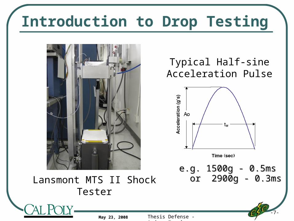
e.g. 1500g - 0.5mse.g. 1500g - 0.5ms or 2900g - 0.3msor 2900g - 0.3msLansmont MTS II Shock Tester
Typical Half-sineAcceleration Pulse
-8-Thesis Defense - Andrew FarrisMay 23, 2008
Drop Impact Reliability
Drop impact reliability testing evaluates the reliability of electronics when subjected to mechanical shock
• Shock causes vibration, PWB bending, and resulting mechanical stresses on solder joints
Generally focused on lead-free solder usage in consumer electronics (handheld products)• Due to governmental regulations pushing toward a
world-wide lead-free market for these products
-9-Thesis Defense - Andrew FarrisMay 23, 2008
Introduction to Drop Testing
The drop impact test• Is repeated until failure occurs
• Determines how many drop impacts of a specific intensity (acceleration peak and duration) can be survived before the device fails
Drop impact reliability data is a tool that can guide designers in developing more robust electronic products
-10-Thesis Defense - Andrew FarrisMay 23, 2008
Drop Impact Demo

-11-Thesis Defense - Andrew FarrisMay 23, 2008
Why Study Lead-free Solder?
Environmental regulations and directives currently restrict the use of lead in consumer electronics products within global markets• European Union’s Restriction of Hazardous
Substances (RoHS)
• China’s Regulation for Pollution Control of Electronics Products (RPCEP)
• And more…
-12-Thesis Defense - Andrew FarrisMay 23, 2008
Why Study Lead-free Solder?
Lead-free solder is still very new to the electronics industry• RoHS regulations took effect in 2006
Many lead-free solder alloys can be used to replace tin-lead solder, and more information is needed on their performance
-13-Thesis Defense - Andrew FarrisMay 23, 2008
Prior Work
Researchers have studied• Lead-free SnAgCu solder alloys and various micro-
additives in the alloys to improve reliability
• Use of underfill and Corner Bonding to improve mechanical strength and reliability of components
• Board and device level drop impact reliability, acceleration, stress, and strain on solder joints for many component and solder joint sizes
-14-Thesis Defense - Andrew FarrisMay 23, 2008
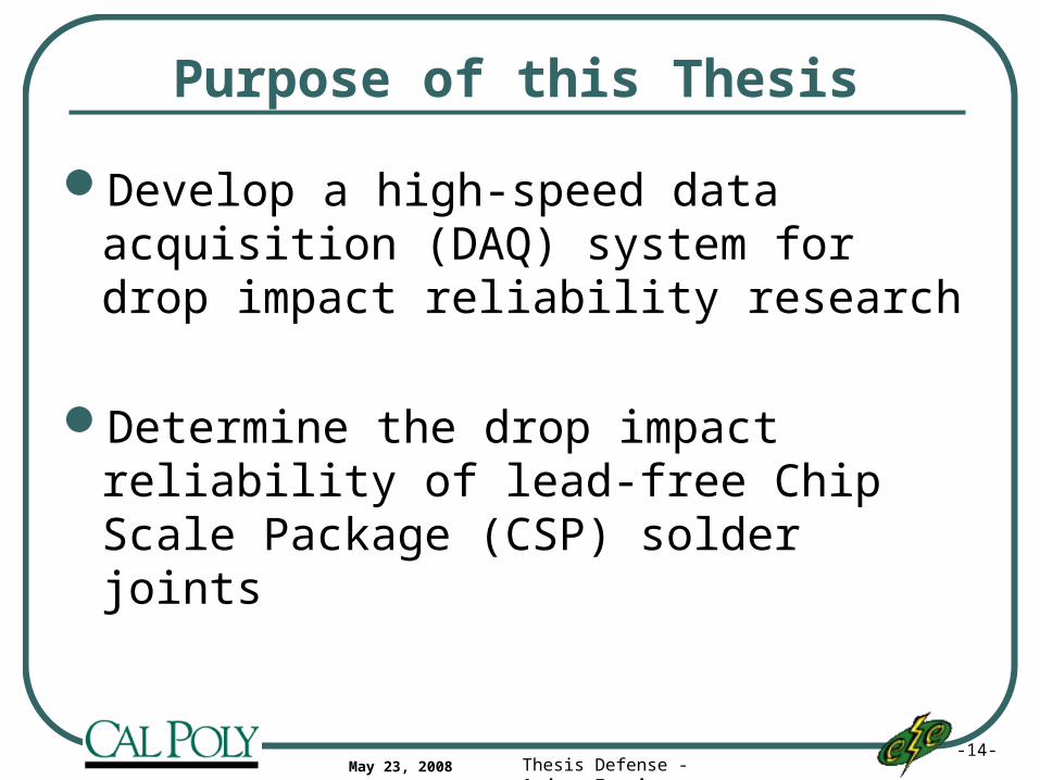
Purpose of this Thesis
Develop a high-speed data acquisition (DAQ) system for drop impact reliability research
Determine the drop impact reliability of lead-free Chip Scale Package (CSP) solder joints
-15-Thesis Defense - Andrew FarrisMay 23, 2008
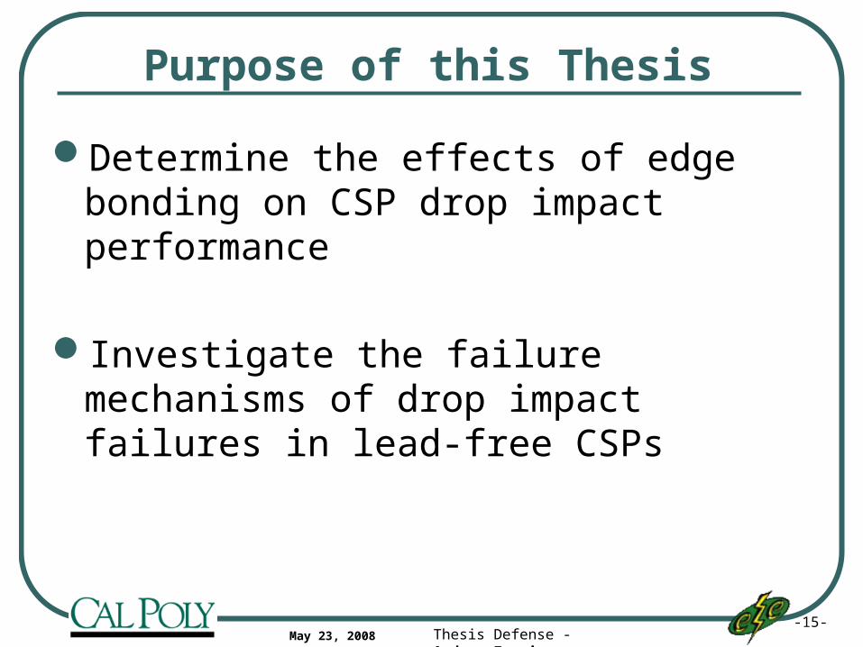
Purpose of this Thesis
Determine the effects of edge bonding on CSP drop impact performance
Investigate the failure mechanisms of drop impact failures in lead-free CSPs
-16-Thesis Defense - Andrew FarrisMay 23, 2008
Agenda
Introduction• Drop Impact Reliability
• Prior Work
• Thesis Research Goals
Failure Detection Systems• Data Acquisition System Design
• Post-drop Resistance Measurement
Test Vehicle Design and Assembly
-17-Thesis Defense - Andrew FarrisMay 23, 2008
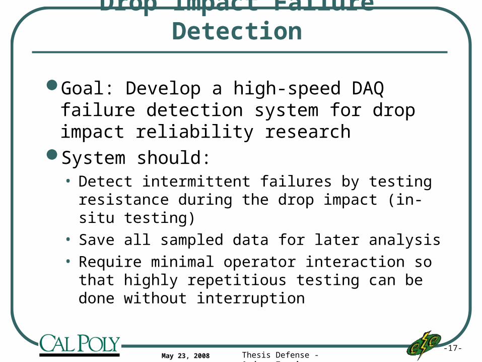
Drop Impact Failure Detection
Goal: Develop a high-speed DAQ failure detection system for drop impact reliability research
System should:• Detect intermittent failures by testing resistance
during the drop impact (in-situ testing)
• Save all sampled data for later analysis
• Require minimal operator interaction so that highly repetitious testing can be done without interruption
-18-Thesis Defense - Andrew FarrisMay 23, 2008
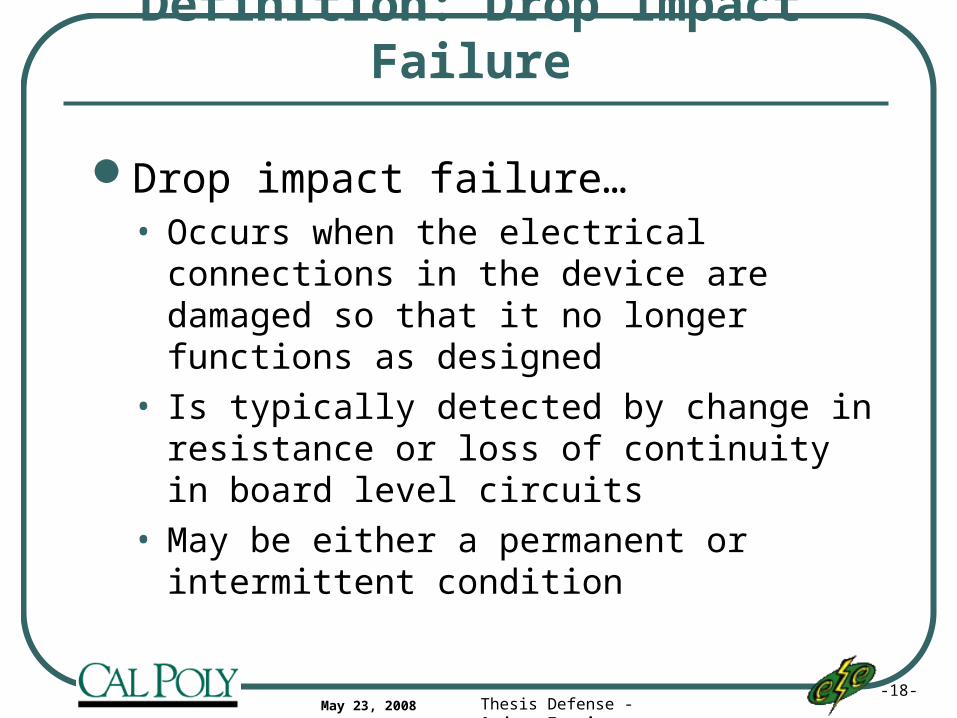
Definition: Drop Impact Failure
Drop impact failure…• Occurs when the electrical connections in the
device are damaged so that it no longer functions as designed
• Is typically detected by change in resistance or loss of continuity in board level circuits
• May be either a permanent or intermittent condition
-19-Thesis Defense - Andrew FarrisMay 23, 2008
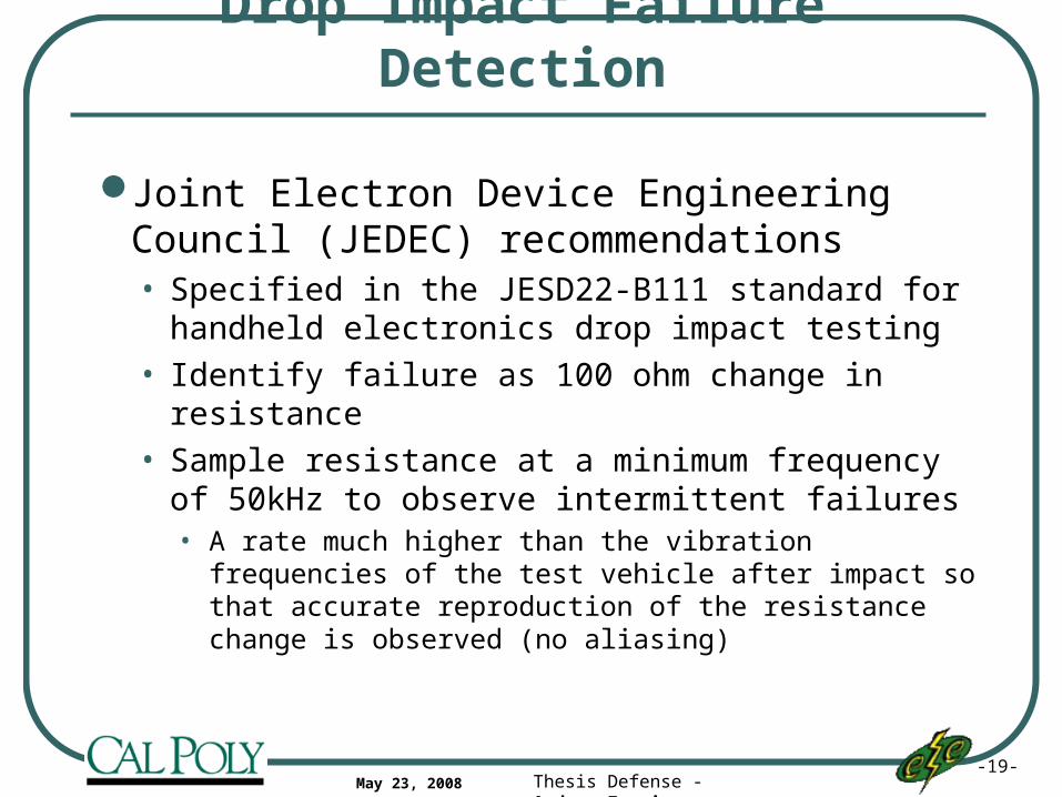
Drop Impact Failure Detection
Joint Electron Device Engineering Council (JEDEC) recommendations• Specified in the JESD22-B111 standard for
handheld electronics drop impact testing
• Identify failure as 100 ohm change in resistance
• Sample resistance at a minimum frequency of 50kHz to observe intermittent failures• A rate much higher than the vibration frequencies of the
test vehicle after impact so that accurate reproduction of the resistance change is observed (no aliasing)
-20-Thesis Defense - Andrew FarrisMay 23, 2008
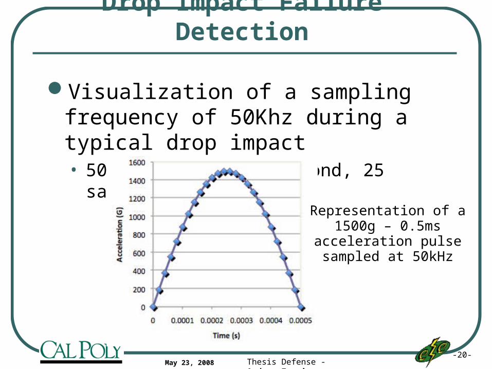
Drop Impact Failure Detection
Visualization of a sampling frequency of 50Khz during a typical drop impact• 50000 samples per second, 25 samples per 0.5ms
Representation of a1500g – 0.5ms
acceleration pulsesampled at 50kHz
-21-Thesis Defense - Andrew FarrisMay 23, 2008
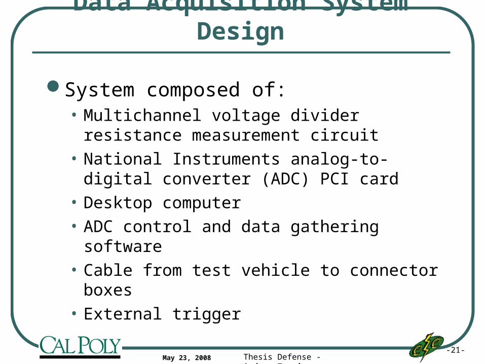
Data Acquisition System Design
System composed of:• Multichannel voltage divider resistance
measurement circuit
• National Instruments analog-to-digital converter (ADC) PCI card
• Desktop computer
• ADC control and data gathering software
• Cable from test vehicle to connector boxes
• External trigger
-22-Thesis Defense - Andrew FarrisMay 23, 2008
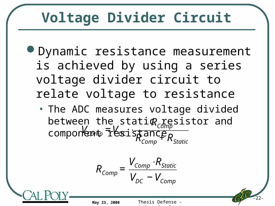
Voltage Divider Circuit
Dynamic resistance measurement is achieved by using a series voltage divider circuit to relate voltage to resistance• The ADC measures voltage divided between the
static resistor and component resistance
€
RComp =VComp ⋅RStaticVDC − VComp€
VComp =VDC ⋅RComp
RComp + RStatic
-23-Thesis Defense - Andrew FarrisMay 23, 2008
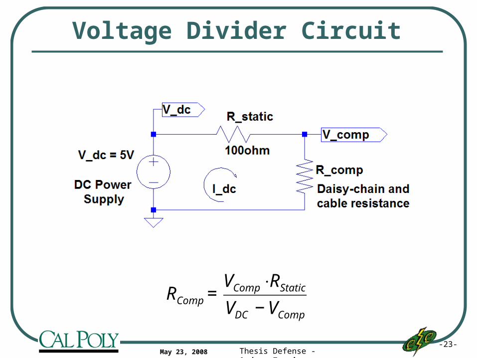
Voltage Divider Circuit
€
RComp =VComp ⋅RStaticVDC − VComp
-24-Thesis Defense - Andrew FarrisMay 23, 2008
Voltage Divider Circuit
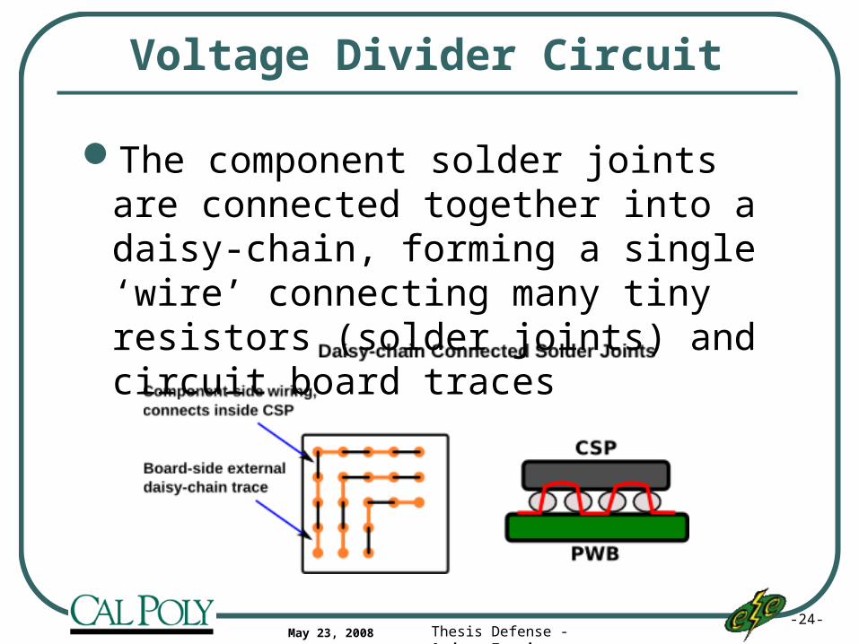
The component solder joints are connected together into a daisy-chain, forming a single ‘wire’ connecting many tiny resistors (solder joints) and circuit board traces

-25-Thesis Defense - Andrew FarrisMay 23, 2008
Voltage Divider and Connector Boxes
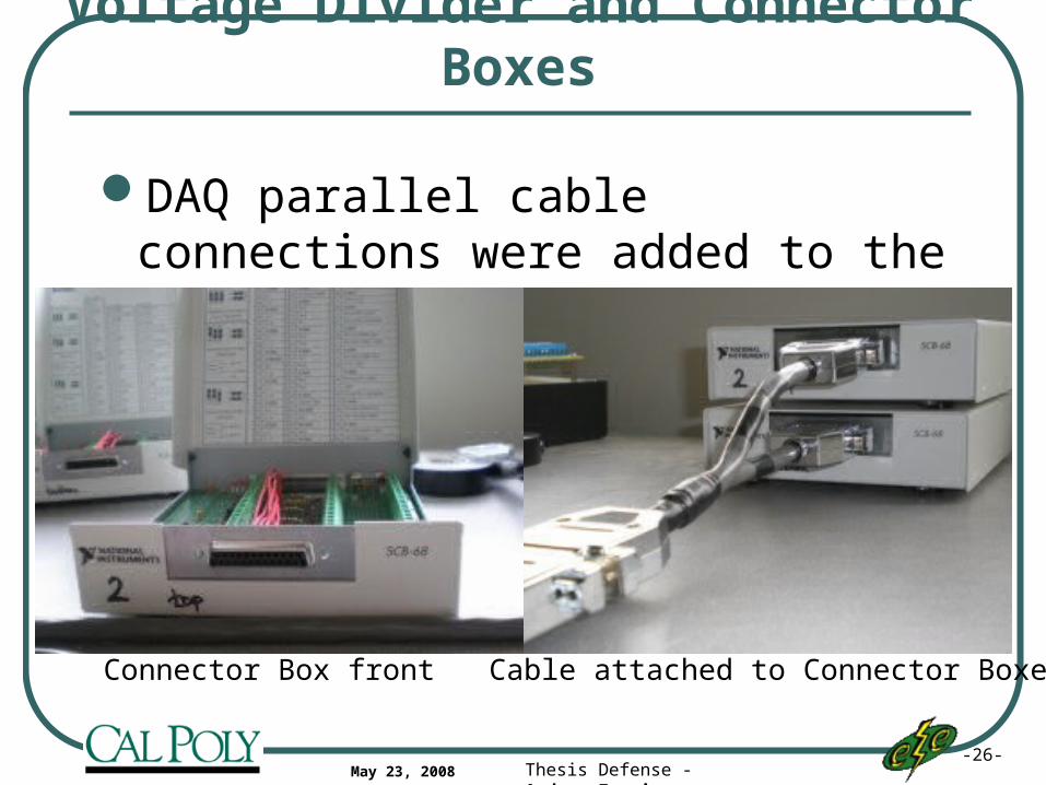
The voltage divider circuit is assembled within two National Instruments connector boxes
-26-Thesis Defense - Andrew FarrisMay 23, 2008
Voltage Divider and Connector Boxes
DAQ parallel cable connections were added to the front of these boxes
Connector Box front Cable attached to Connector Boxes

-27-Thesis Defense - Andrew FarrisMay 23, 2008
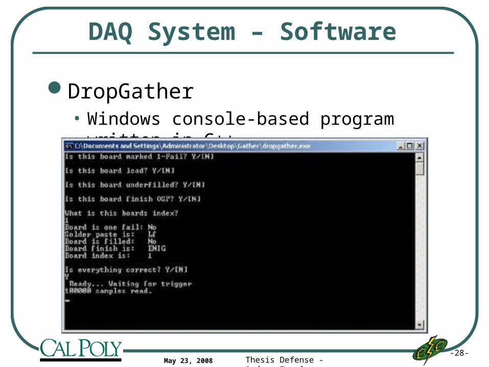
DAQ System – Software
DropGather• Windows console-based program written in C++
• Interfaces to National Instruments DAQmx driver libraries for ADC device control
• Released as open source software for others to use as an example in building similar systems
-28-Thesis Defense - Andrew FarrisMay 23, 2008
DAQ System – Software
DropGather• Windows console-based program written in C++
-29-Thesis Defense - Andrew FarrisMay 23, 2008
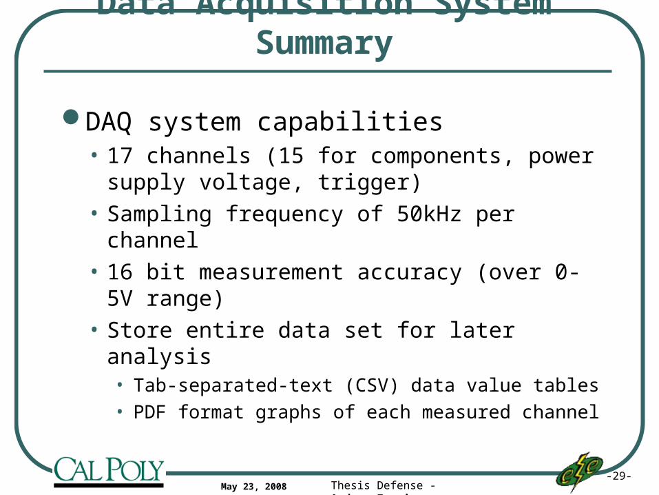
Data Acquisition System Summary
DAQ system capabilities• 17 channels (15 for components, power supply
voltage, trigger)
• Sampling frequency of 50kHz per channel
• 16 bit measurement accuracy (over 0-5V range)
• Store entire data set for later analysis• Tab-separated-text (CSV) data value tables
• PDF format graphs of each measured channel
-30-Thesis Defense - Andrew FarrisMay 23, 2008
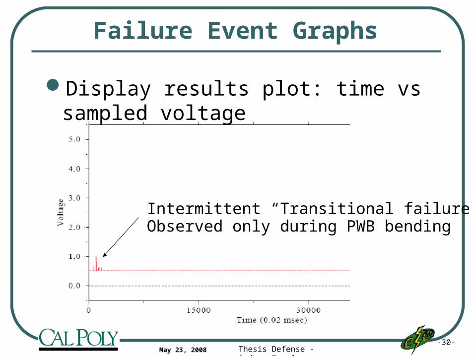
Failure Event Graphs
Display results plot: time vs sampled voltage
Intermittent “Transitional failure”Observed only during PWB bending
30
-31-Thesis Defense - Andrew FarrisMay 23, 2008
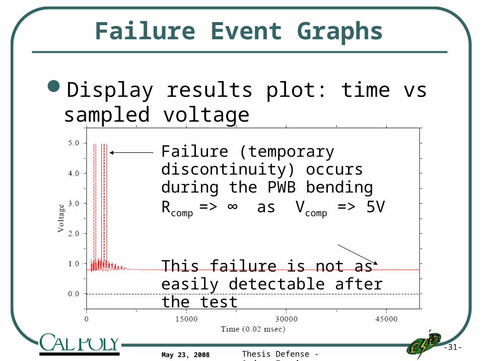
Failure Event Graphs
Display results plot: time vs sampled voltage
Failure (temporary discontinuity) occurs during the PWB bendingRcomp => ∞ as Vcomp => 5V
This failure is not as easily detectable after the test
31
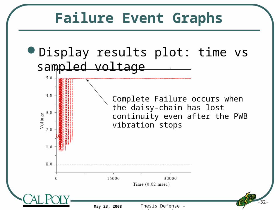
-32-Thesis Defense - Andrew FarrisMay 23, 2008
Failure Event Graphs
Display results plot: time vs sampled voltage
Complete Failure occurs when the daisy-chain has lost continuity even after the PWB vibration stops
32
-33-Thesis Defense - Andrew FarrisMay 23, 2008
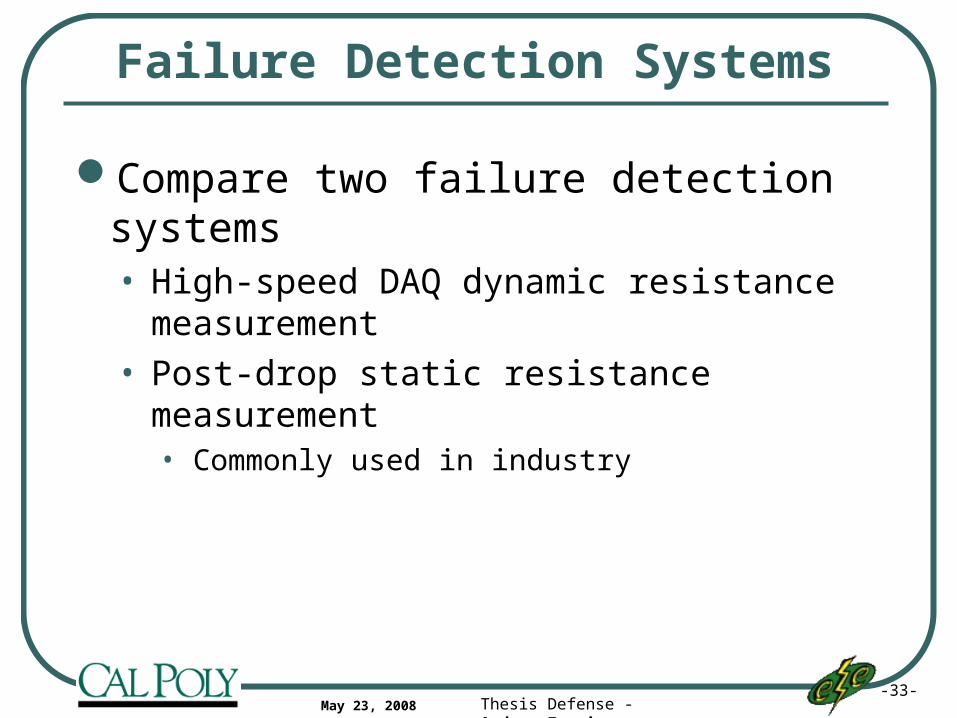
Failure Detection Systems
Compare two failure detection systems• High-speed DAQ dynamic resistance measurement
• Post-drop static resistance measurement• Commonly used in industry
-34-Thesis Defense - Andrew FarrisMay 23, 2008
Post-Drop Testing
Uses a single resistance measurement per drop taken after the board vibration ceases
Failure when a 10 ohm static rise is detectedMonitor resistance change over multiple drop
periodLabView program which configures Keithley
equipment to collect resistance valuesOutputs tabular data for resistance of all 15
components once each drop34
-35-Thesis Defense - Andrew FarrisMay 23, 2008
Post-Drop Testing
Advantage:• No wires soldered to the test board, fast setup
• Low cost system
Disadvantages:• Cannot test in-situ (during board deflection and
vibration conditions)
• Requires operator interaction every drop cycle
• Only one test per drop provides fairly poor resolution for when failure occurs
-36-Thesis Defense - Andrew FarrisMay 23, 2008
Agenda
Introduction• Drop Impact Reliability
• Prior Work
• Thesis Research Goals
Failure Detection Systems• Data Acquisition System Design
• Post-drop Resistance Measurement
Test Vehicle Design and Assembly
-37-Thesis Defense - Andrew FarrisMay 23, 2008
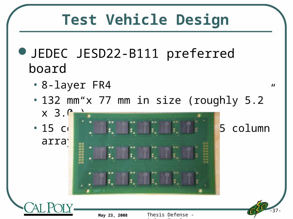
Test Vehicle Design
JEDEC JESD22-B111 preferred board• 8-layer FR4
• 132 mm x 77 mm in size (roughly 5.2” x 3.0”)
• 15 components in a 3 row by 5 column array
-38-Thesis Defense - Andrew FarrisMay 23, 2008
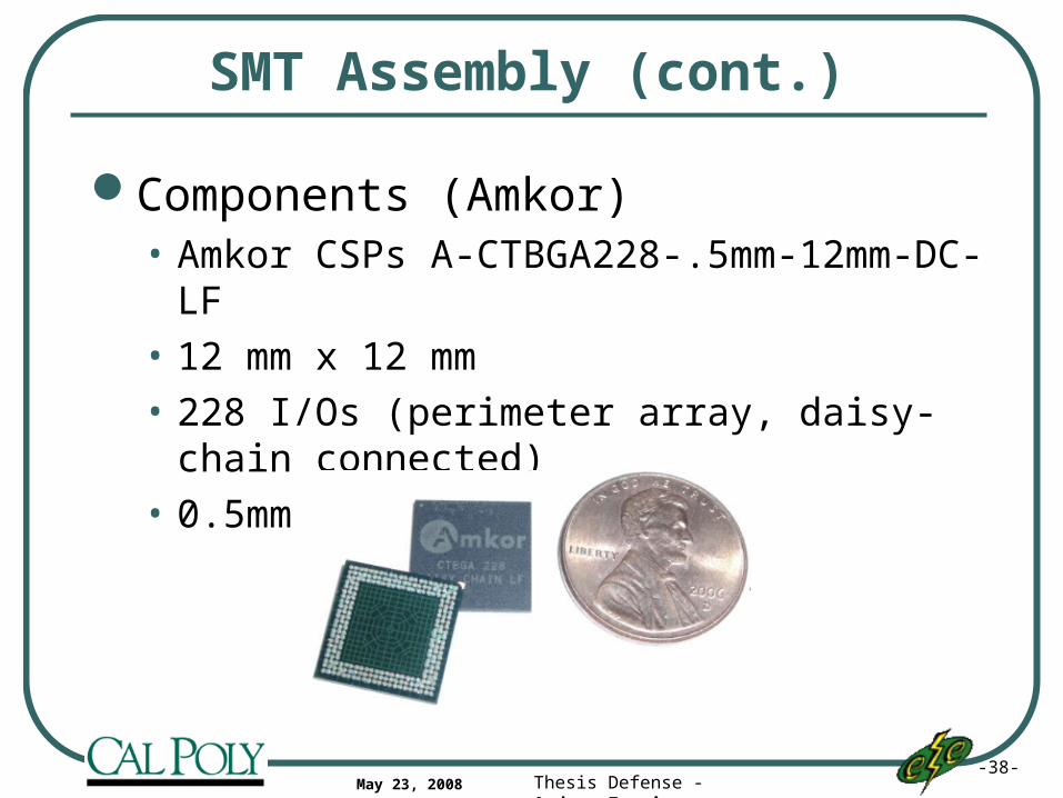
SMT Assembly (cont.)
Components (Amkor)• Amkor CSPs A-CTBGA228-.5mm-12mm-DC-LF
• 12 mm x 12 mm
• 228 I/Os (perimeter array, daisy-chain connected)
• 0.5mm pitch
-39-Thesis Defense - Andrew FarrisMay 23, 2008
SMT Assembly (cont.)
Lead-free Solder Paste• Multicore 318 LF 97SC
• SnAg3.0Cu0.5 alloy composition (also called SAC305)
• Primarily tin with 3.0% silver and 0.5% copper by weight
• Common replacement for tin-lead solder
-40-Thesis Defense - Andrew FarrisMay 23, 2008
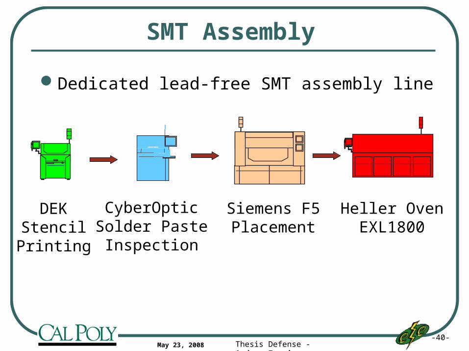
SE 300
SMT Assembly
DEKStencilPrinting
CyberOpticSolder PasteInspection
Siemens F5Placement
Heller OvenEXL1800
Dedicated lead-free SMT assembly line
-41-Thesis Defense - Andrew FarrisMay 23, 2008
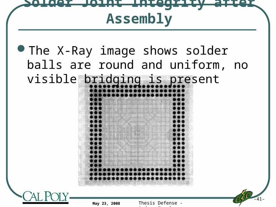
Solder Joint Integrity after Assembly
The X-Ray image shows solder balls are round and uniform, no visible bridging is present
-42-Thesis Defense - Andrew FarrisMay 23, 2008
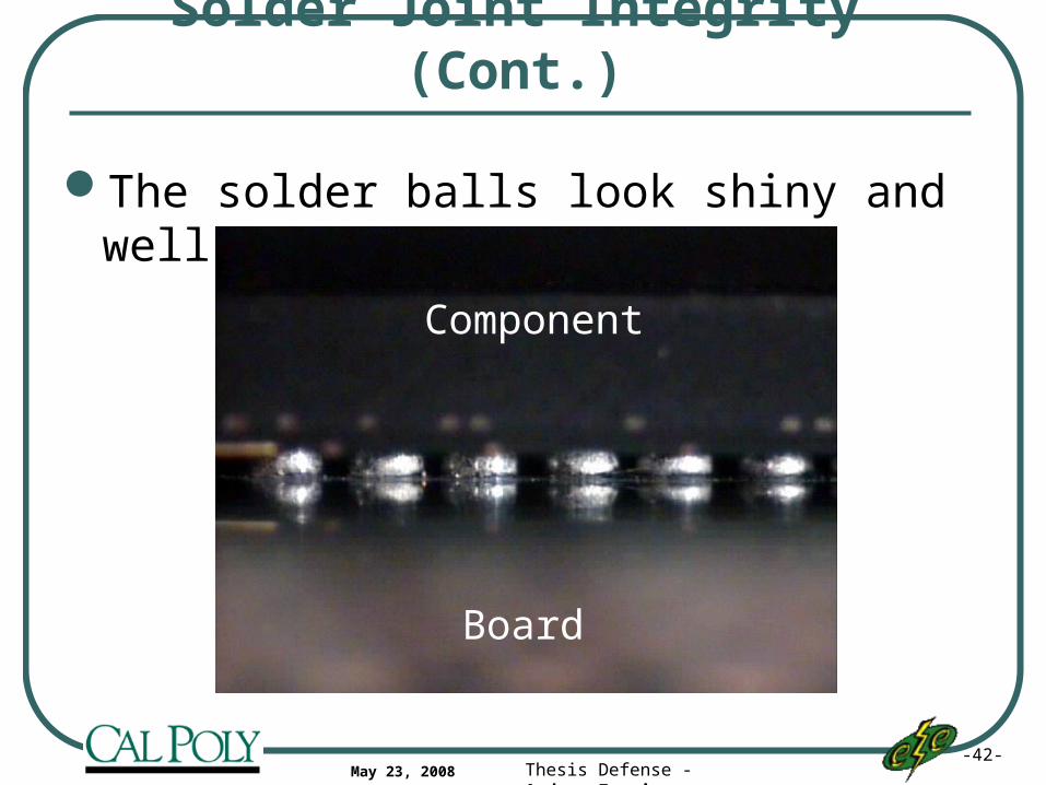
Solder Joint Integrity (Cont.)
The solder balls look shiny and well collapsed
Component
Board
-43-Thesis Defense - Andrew FarrisMay 23, 2008
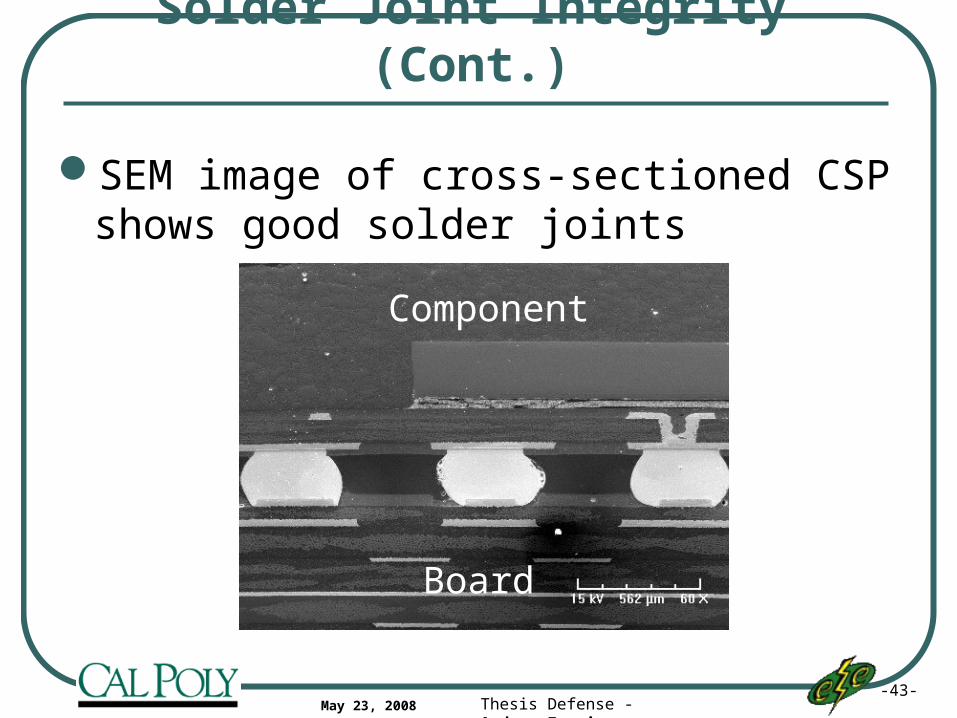
Solder Joint Integrity (Cont.)
SEM image of cross-sectioned CSP shows good solder joints
Component
Board
-44-Thesis Defense - Andrew FarrisMay 23, 2008
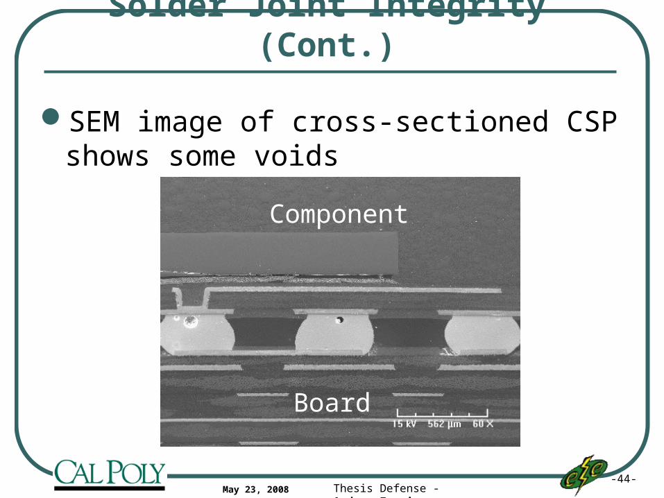
Solder Joint Integrity (Cont.)
SEM image of cross-sectioned CSP shows some voids
Component
Board
-45-Thesis Defense - Andrew FarrisMay 23, 2008
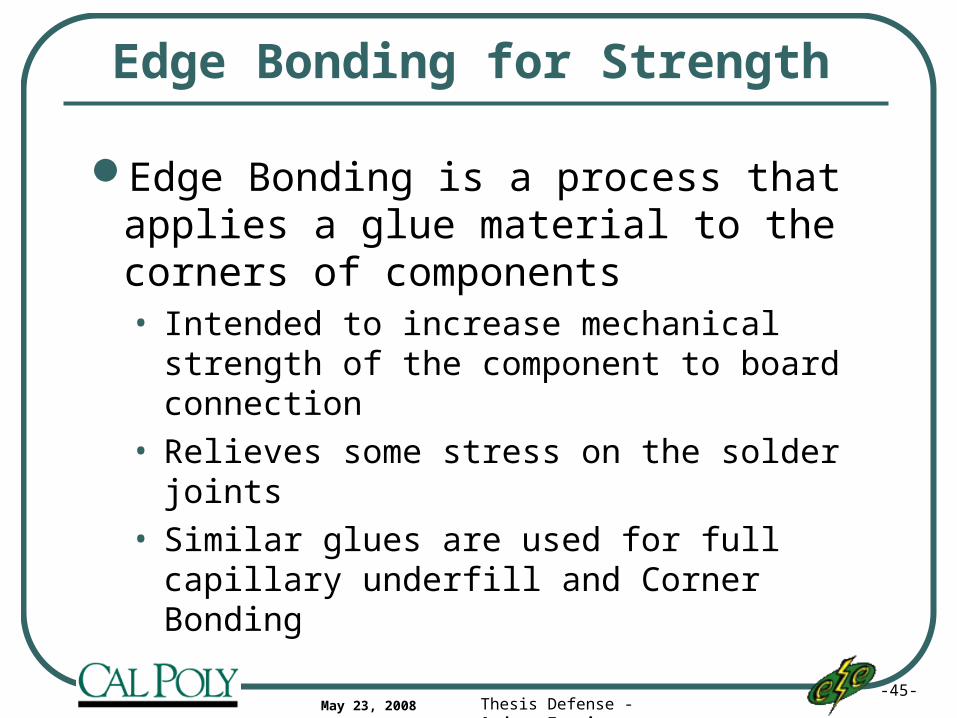
Edge Bonding for Strength
Edge Bonding is a process that applies a glue material to the corners of components• Intended to increase mechanical strength of the
component to board connection
• Relieves some stress on the solder joints
• Similar glues are used for full capillary underfill and Corner Bonding
-46-Thesis Defense - Andrew FarrisMay 23, 2008
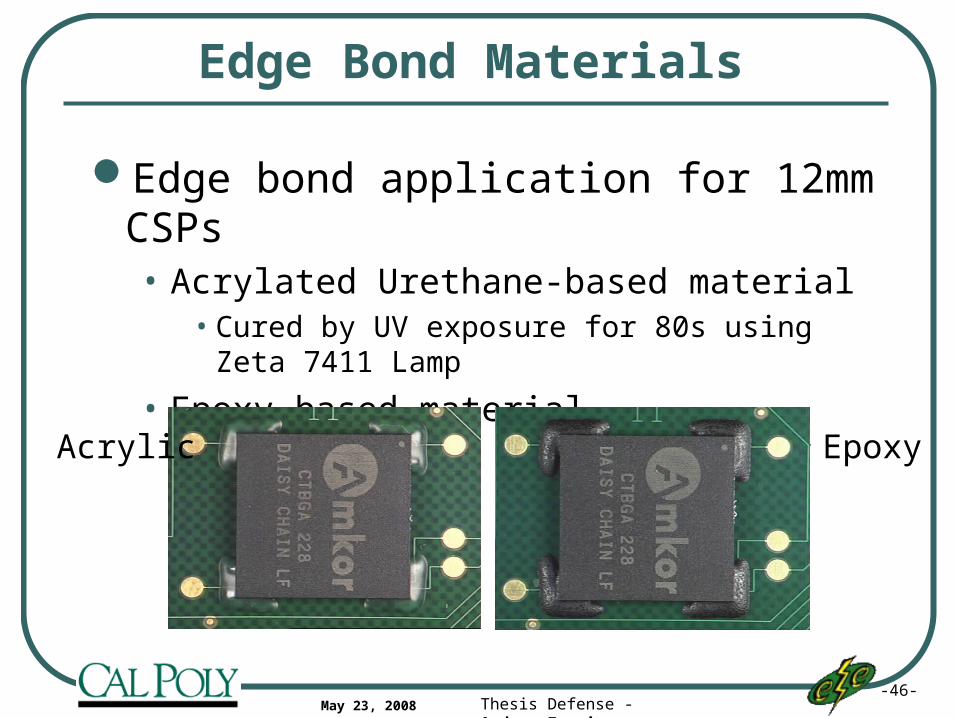
Edge Bond Materials
Edge bond application for 12mm CSPs• Acrylated Urethane-based material
• Cured by UV exposure for 80s using Zeta 7411 Lamp
• Epoxy-based material• Thermally cured for 20min in 80° C oven
EpoxyAcrylic
-47-Thesis Defense - Andrew FarrisMay 23, 2008
Agenda
Drop Impact TestingAnalysis
• Reliability Data
• Failure Mechanisms
• Acceleration on Test Vehicle
ConclusionsAcknowledgements
-48-Thesis Defense - Andrew FarrisMay 23, 2008
Reliability Test Design
Drop tests were conducted at Henkel Electronics in Irvine, CA, during Summer ‘07 internship• This is a Henkel Corporation R&D facility focused
on adhesives, packaging, and bonding agents
-49-Thesis Defense - Andrew FarrisMay 23, 2008
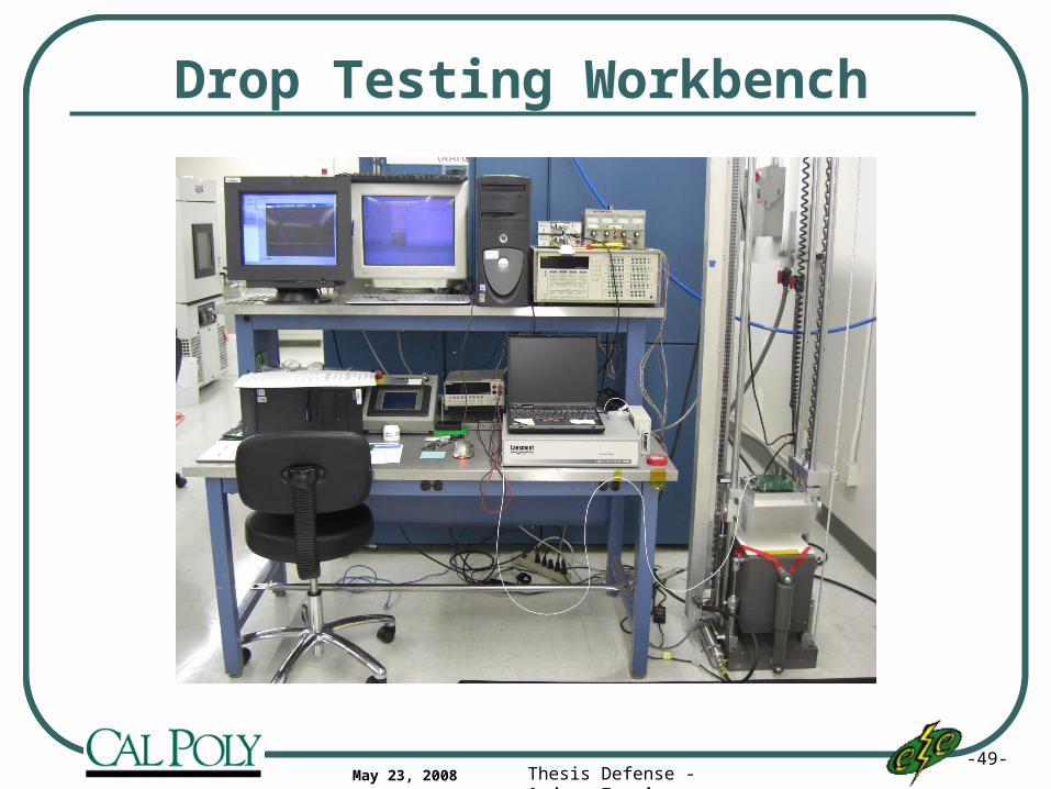
Drop Testing Workbench
-50-Thesis Defense - Andrew FarrisMay 23, 2008
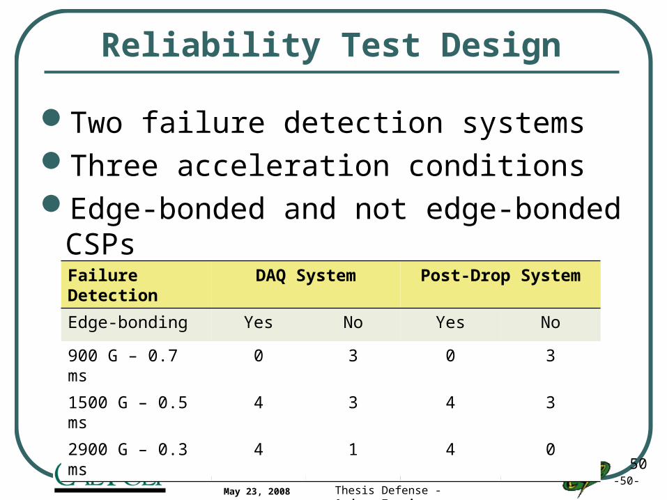
Reliability Test Design
Two failure detection systemsThree acceleration conditionsEdge-bonded and not edge-bonded CSPs
Failure Detection DAQ System Post-Drop System
Edge-bonding Yes No Yes No
900 G – 0.7 ms 0 3 0 3
1500 G – 0.5 ms 4 3 4 3
2900 G – 0.3 ms 4 1 4 0
50
-51-Thesis Defense - Andrew FarrisMay 23, 2008
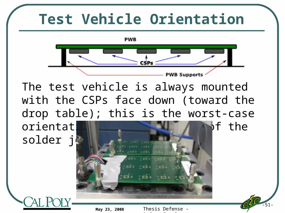
Test Vehicle Orientation
The test vehicle is always mounted with the CSPs face down (toward the drop table); this is the worst-case orientation for reliability of the solder joints

-52-Thesis Defense - Andrew FarrisMay 23, 2008
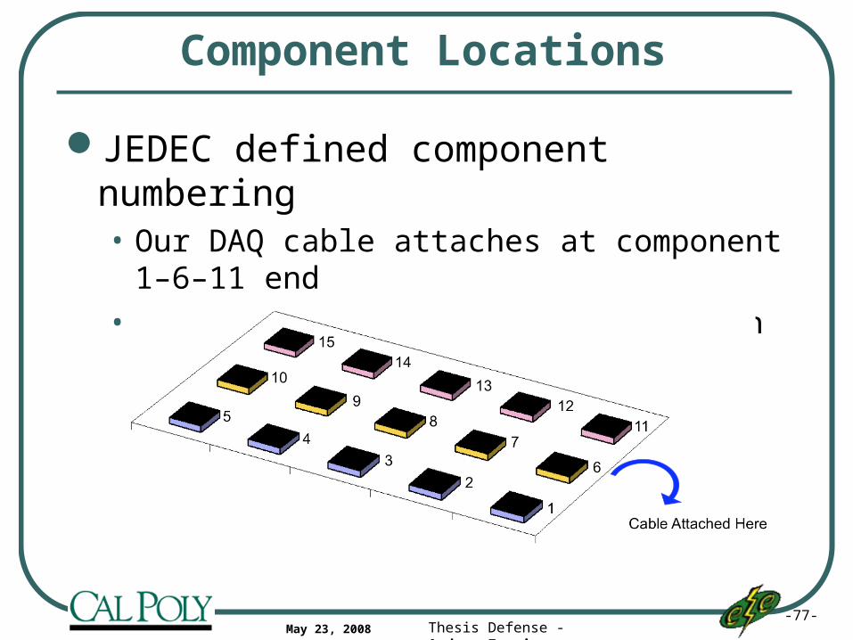
Component Locations
JEDEC defined component numbering• Our DAQ cable attaches at component 1–6–11 end
• As shown components are underneath board
-53-Thesis Defense - Andrew FarrisMay 23, 2008
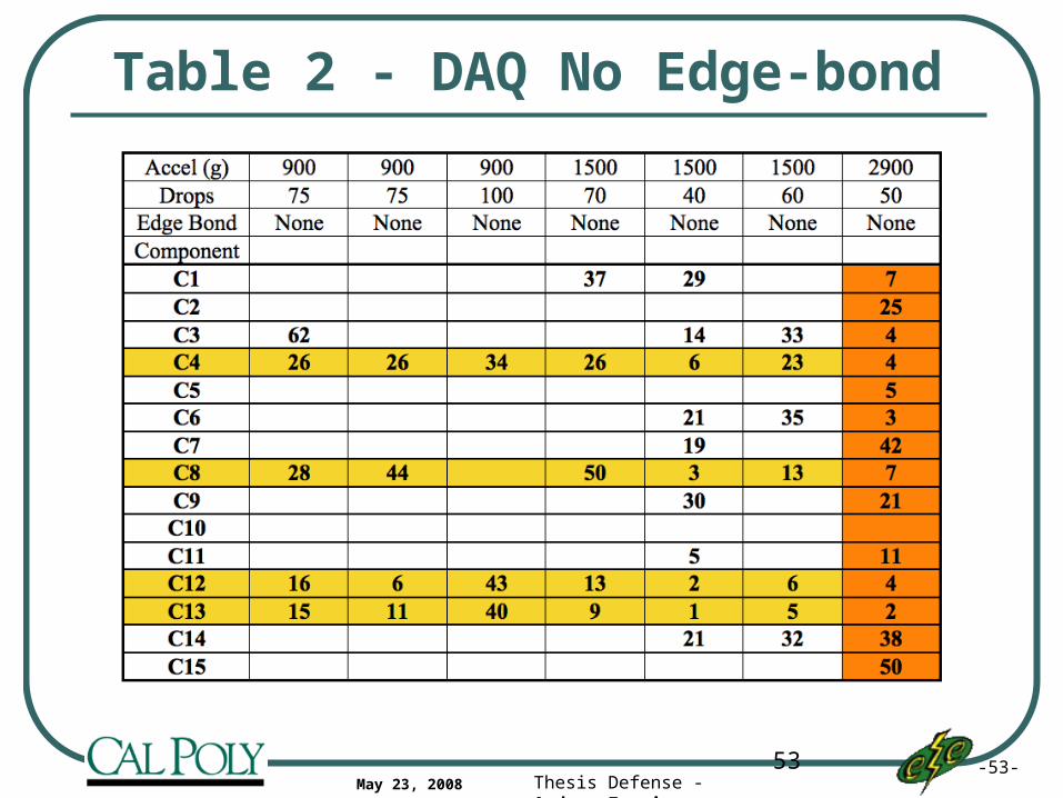
Table 2 - DAQ No Edge-bond
53
-54-Thesis Defense - Andrew FarrisMay 23, 2008
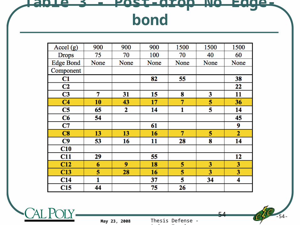
Table 3 - Post-drop No Edge-bond
54
-55-Thesis Defense - Andrew FarrisMay 23, 2008
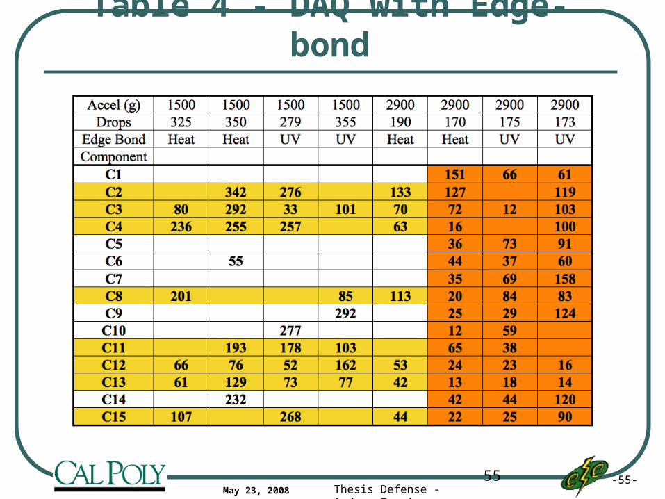
Table 4 - DAQ with Edge-bond
55
-56-Thesis Defense - Andrew FarrisMay 23, 2008
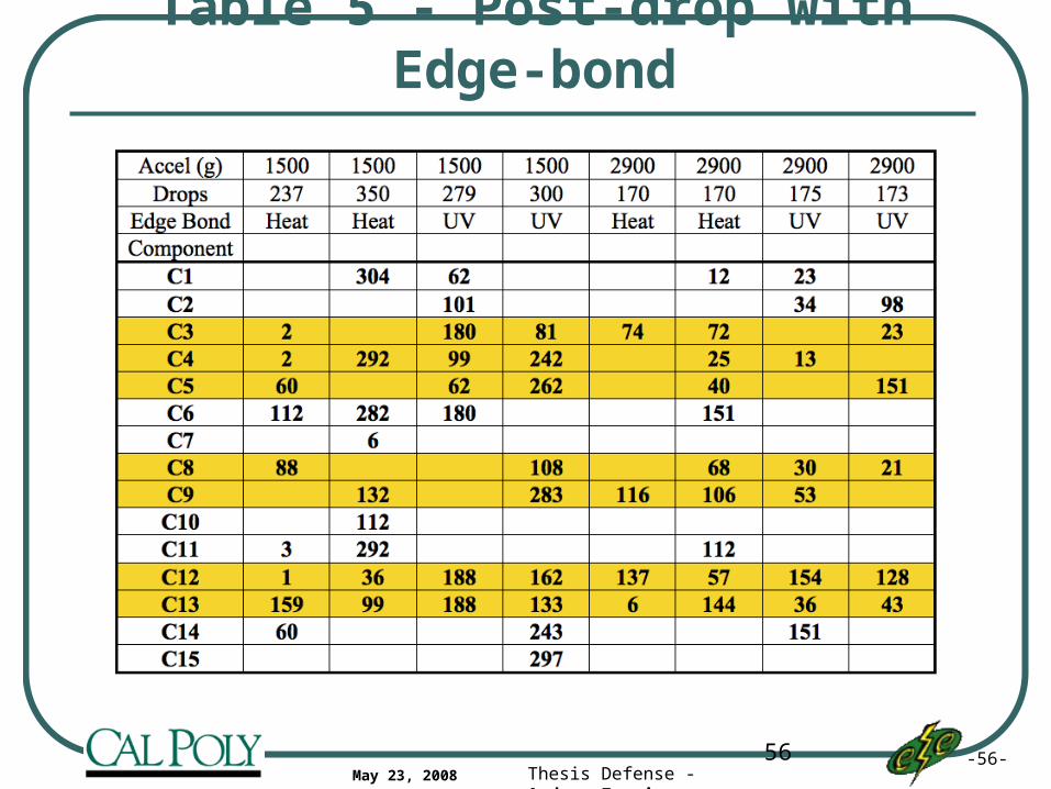
Table 5 - Post-drop with Edge-bond
56
-57-Thesis Defense - Andrew FarrisMay 23, 2008
Agenda
Drop Impact TestingAnalysis
• Reliability Data
• Failure Mechanisms
• Acceleration on Test Vehicle
ConclusionsAcknowledgements
-58-Thesis Defense - Andrew FarrisMay 23, 2008
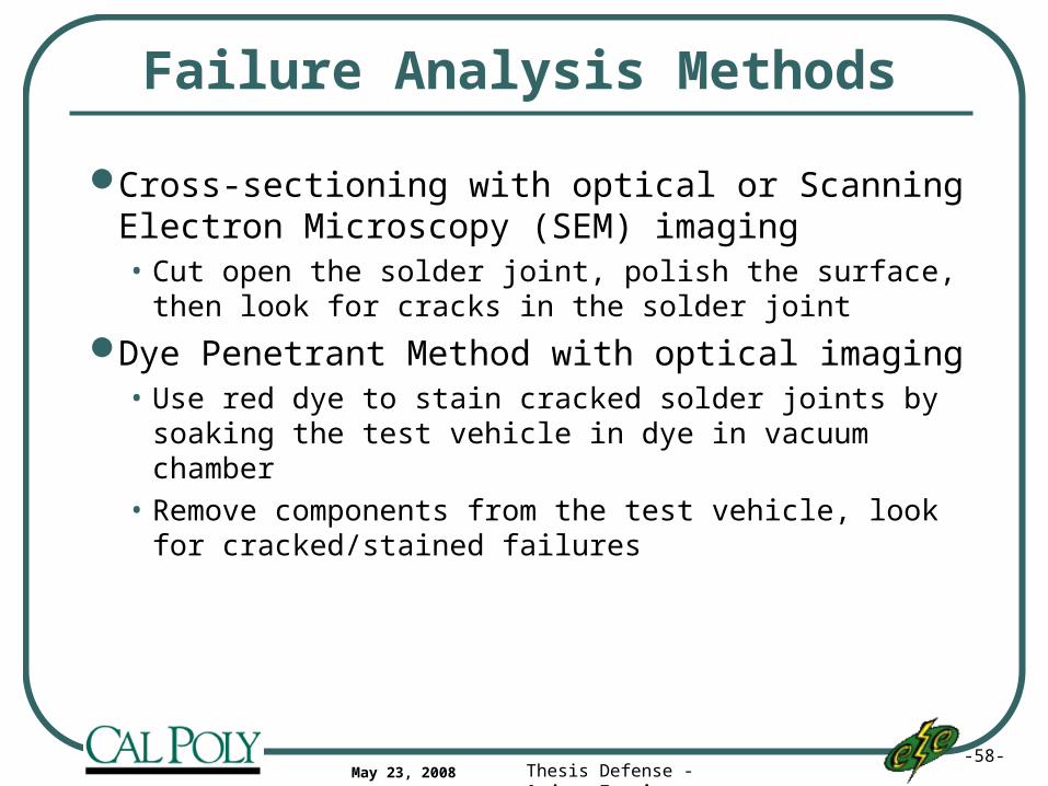
Failure Analysis Methods
Cross-sectioning with optical or Scanning Electron Microscopy (SEM) imaging• Cut open the solder joint, polish the surface, then
look for cracks in the solder joint
Dye Penetrant Method with optical imaging• Use red dye to stain cracked solder joints by soaking
the test vehicle in dye in vacuum chamber• Remove components from the test vehicle, look for
cracked/stained failures
-59-Thesis Defense - Andrew FarrisMay 23, 2008
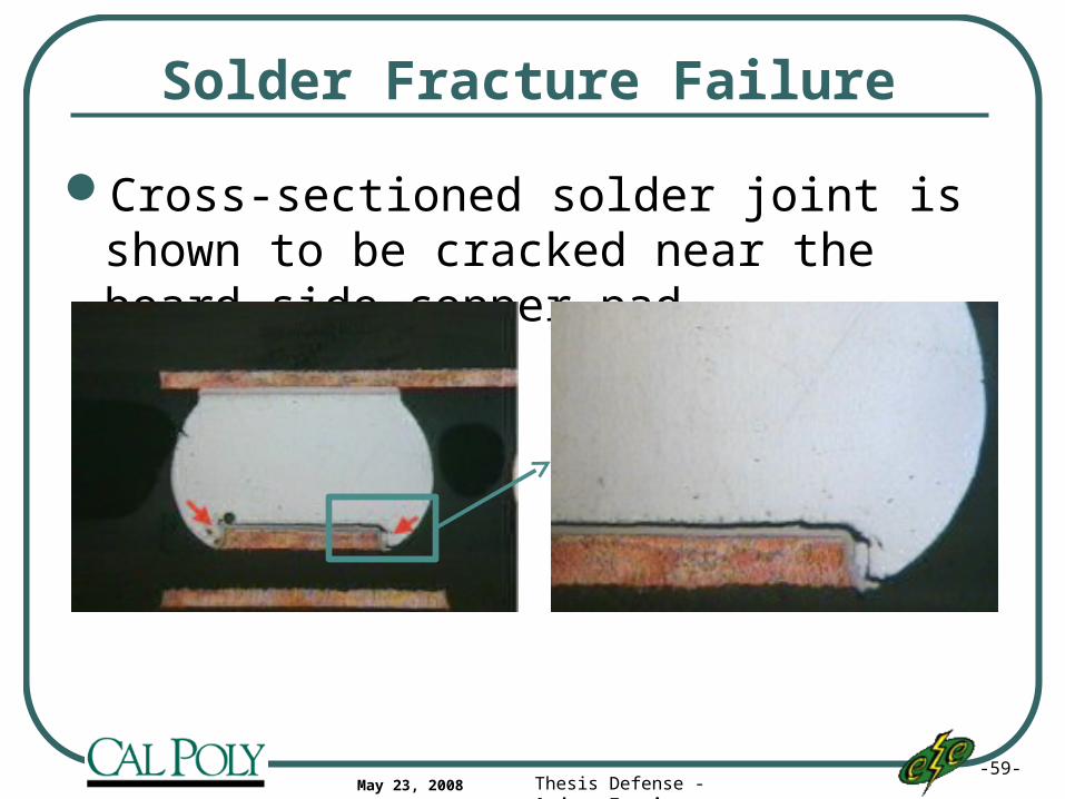
Cross-sectioned solder joint is shown to be cracked near the board side copper pad
Solder Fracture Failure
-60-Thesis Defense - Andrew FarrisMay 23, 2008
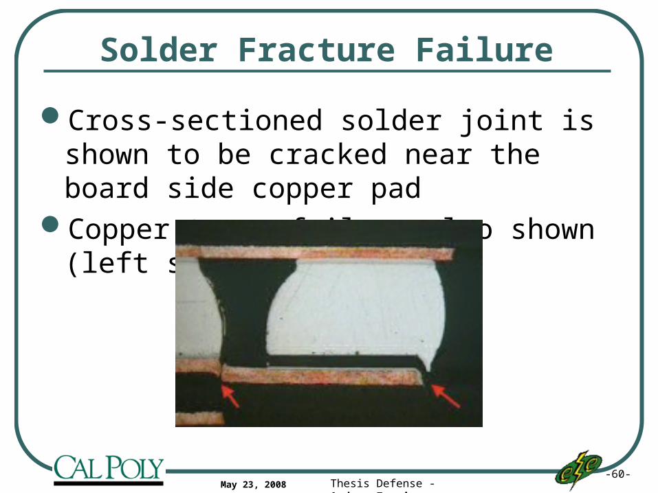
Solder Fracture Failure
Cross-sectioned solder joint is shown to be cracked near the board side copper pad
Copper trace failure also shown (left side)
-61-Thesis Defense - Andrew FarrisMay 23, 2008
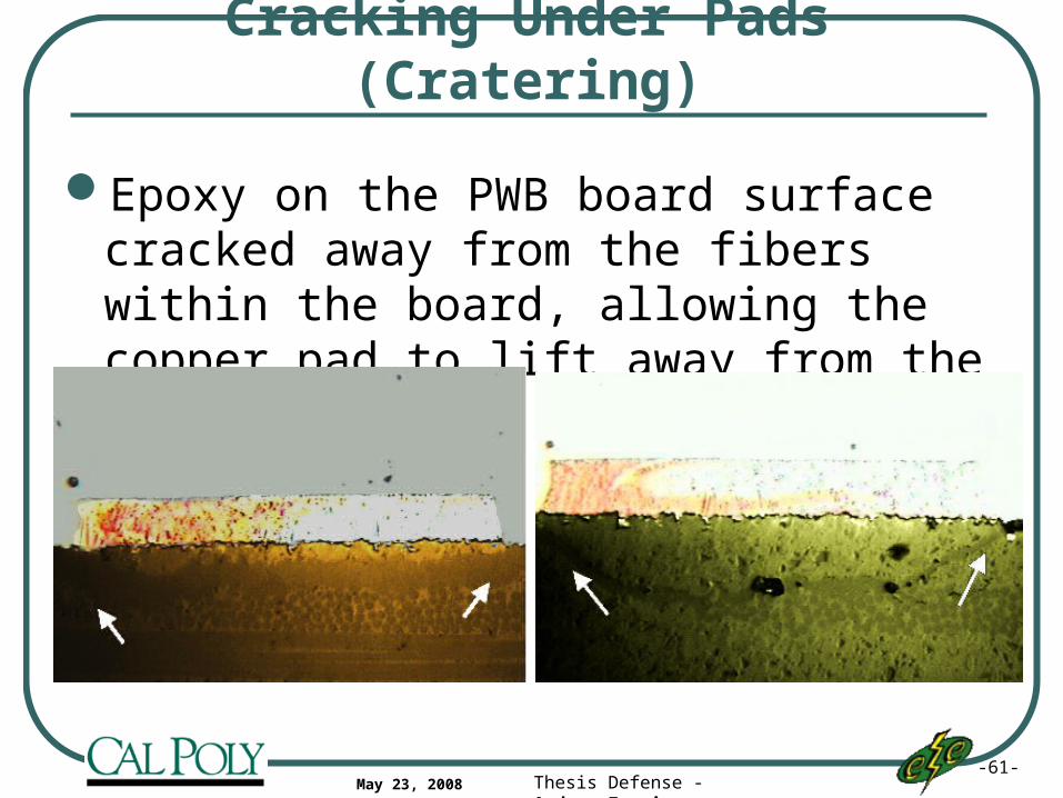
Cracking Under Pads (Cratering)
Epoxy on the PWB board surface cracked away from the fibers within the board, allowing the copper pad to lift away from the board
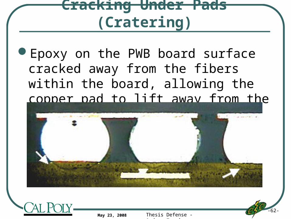
-62-Thesis Defense - Andrew FarrisMay 23, 2008
Epoxy on the PWB board surface cracked away from the fibers within the board, allowing the copper pad to lift away from the board
Cracking Under Pads (Cratering)
-63-Thesis Defense - Andrew FarrisMay 23, 2008
Dye penetrant testing was used to determine the extent of pad cratering problems
Six boards were soaked in dye, then all 15 components were pulled off the boards
Dye stained solder cracks and pad craters were present before the components were pulled off
Cracking Under Pads (Cratering)
-64-Thesis Defense - Andrew FarrisMay 23, 2008
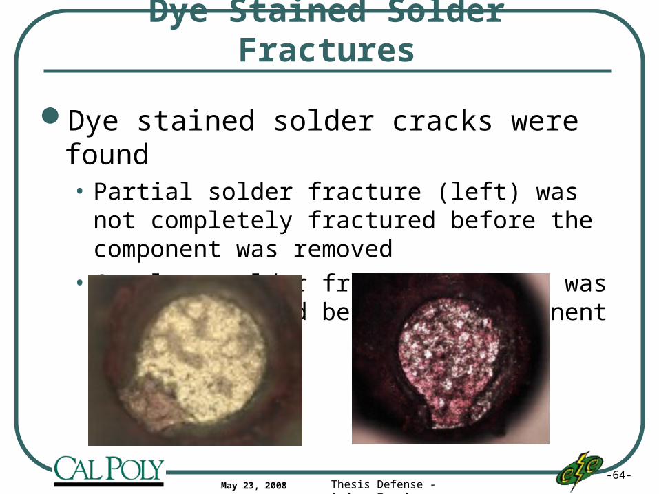
Dye Stained Solder Fractures
Dye stained solder cracks were found• Partial solder fracture (left) was not completely
fractured before the component was removed
• Complete solder fracture (right) was fully fractured before the component was removed
-65-Thesis Defense - Andrew FarrisMay 23, 2008
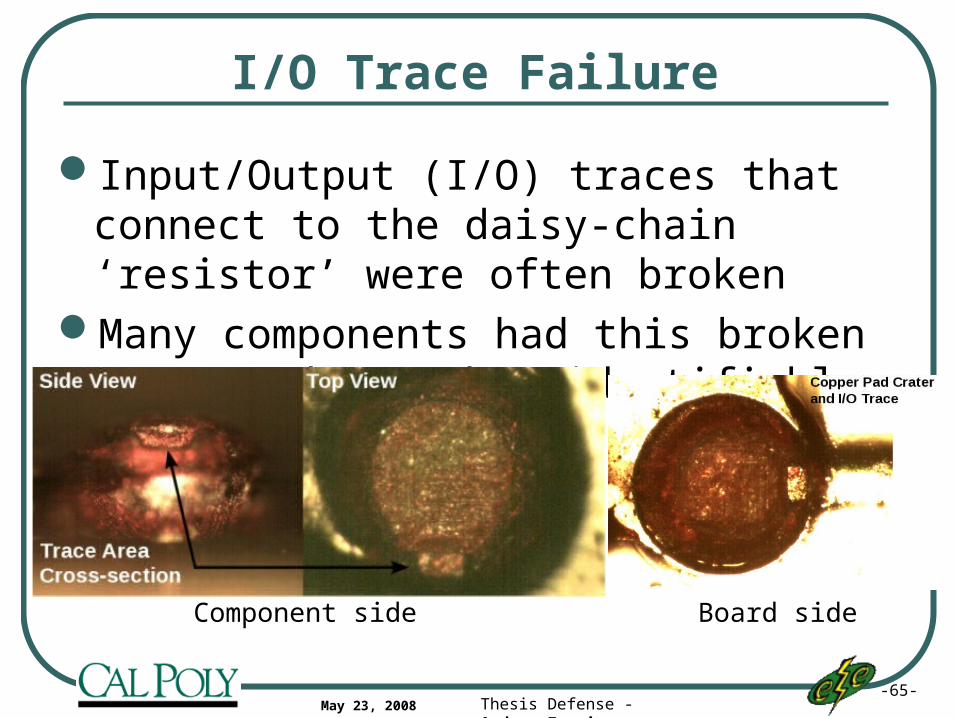
Input/Output (I/O) traces that connect to the daisy-chain ‘resistor’ were often broken
Many components had this broken trace and no other identifiable failure
I/O Trace Failure
Board sideComponent side
-66-Thesis Defense - Andrew FarrisMay 23, 2008
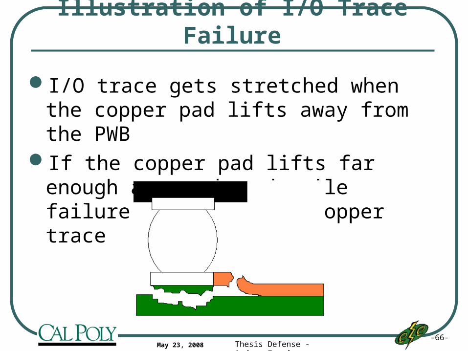
Illustration of I/O Trace Failure
I/O trace gets stretched when the copper pad lifts away from the PWB
If the copper pad lifts far enough away, then ductile failure occurs in the copper trace
-67-Thesis Defense - Andrew FarrisMay 23, 2008
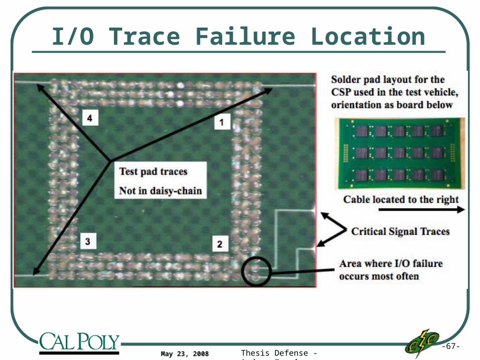
I/O Trace Failure Location
-68-Thesis Defense - Andrew FarrisMay 23, 2008
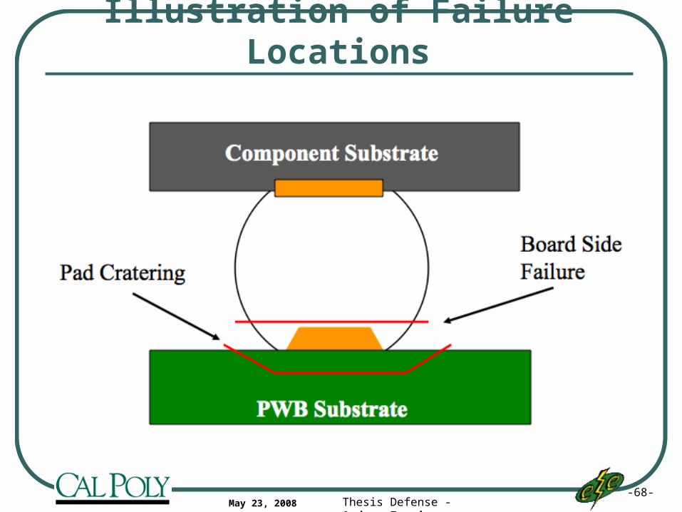
Illustration of Failure Locations
-69-Thesis Defense - Andrew FarrisMay 23, 2008
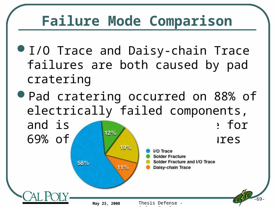
I/O Trace and Daisy-chain Trace failures are both caused by pad cratering
Pad cratering occurred on 88% of electrically failed components, and is directly responsible for 69% of all electrical failures
Failure Mode Comparison
-70-Thesis Defense - Andrew FarrisMay 23, 2008
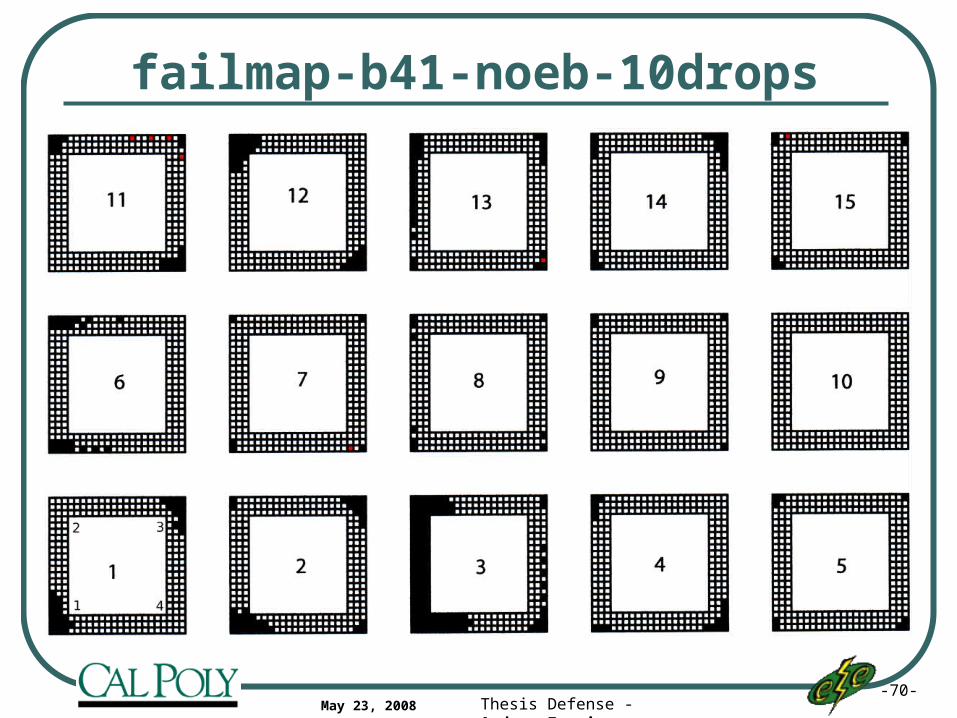
failmap-b41-noeb-10drops
-71-Thesis Defense - Andrew FarrisMay 23, 2008
Agenda
Drop Impact TestingAnalysis
• Reliability Data
• Failure Mechanisms
• Acceleration on Test Vehicle
ConclusionsAcknowledgements
-72-Thesis Defense - Andrew FarrisMay 23, 2008
Cable Influence on PWB Loading
Results from the comparison of failure detection methods• The DAQ system cable attached to the PWB
appears to effects loading conditions
• Fewer components fell off the DAQ tested boards than off the post-drop tested boards
• The earliest component failure locations vary between DAQ and post-drop tested boards
72
-73-Thesis Defense - Andrew FarrisMay 23, 2008
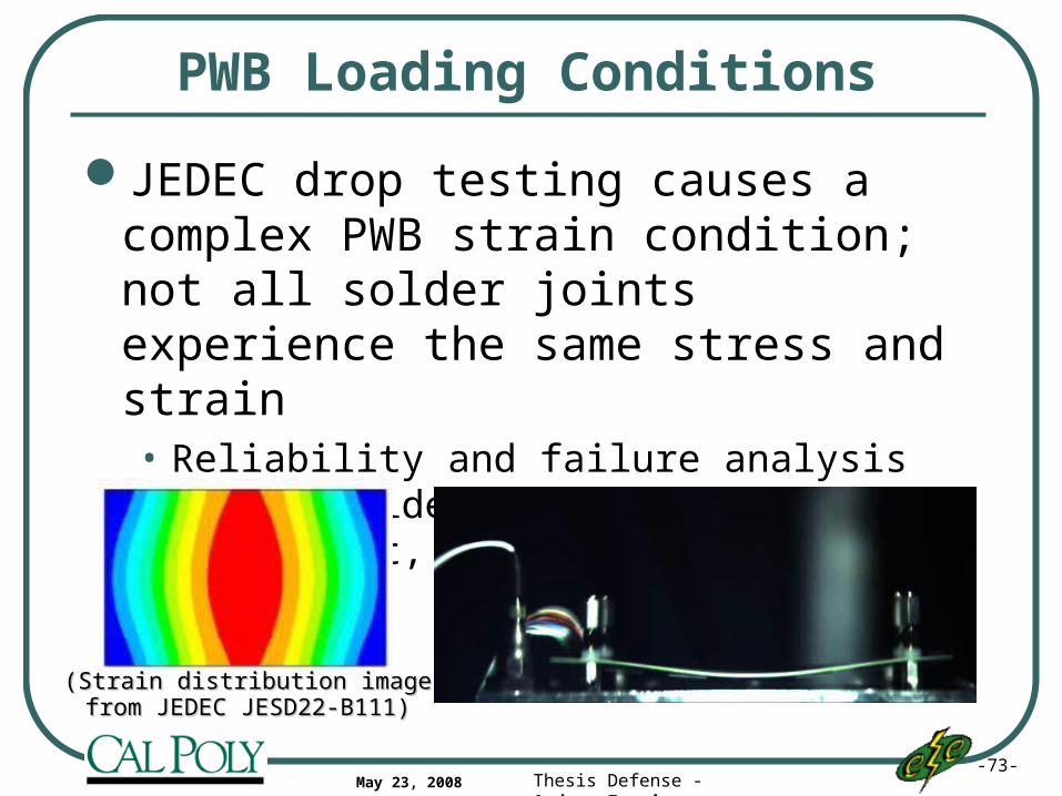
PWB Loading Conditions
JEDEC drop testing causes a complex PWB strain condition; not all solder joints experience the same stress and strain• Reliability and failure analysis must consider
component location, drop count, and acceleration pulse profile
(Strain distribution image(Strain distribution imagefrom JEDEC JESD22-B111)from JEDEC JESD22-B111)
-74-Thesis Defense - Andrew FarrisMay 23, 2008
Local Acceleration Conditions
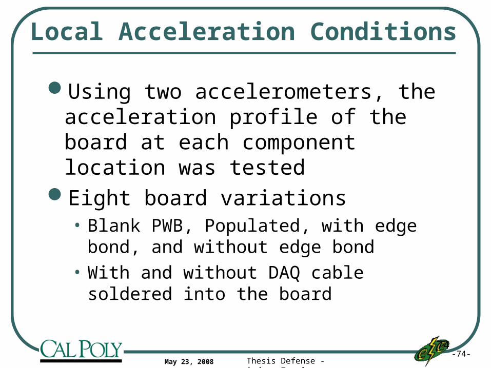
Using two accelerometers, the acceleration profile of the board at each component location was tested
Eight board variations• Blank PWB, Populated, with edge bond, and
without edge bond
• With and without DAQ cable soldered into the board
74
-75-Thesis Defense - Andrew FarrisMay 23, 2008
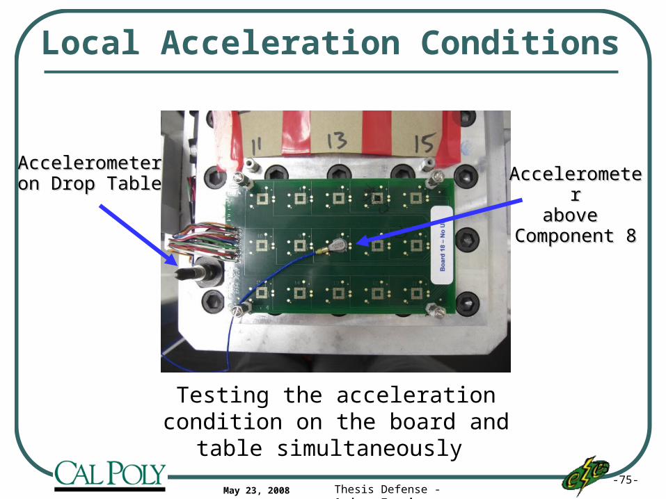
Local Acceleration Conditions
AccelerometerAccelerometerabove above
Component 8Component 8
75
AccelerometerAccelerometeron Drop Tableon Drop Table
Testing the acceleration condition on the board and table simultaneously
-76-Thesis Defense - Andrew FarrisMay 23, 2008
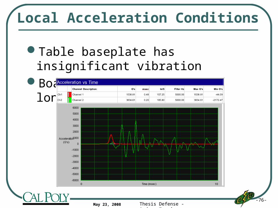
Local Acceleration Conditions
Table baseplate has insignificant vibrationBoard vibrates over period longer than 10ms
76
-77-Thesis Defense - Andrew FarrisMay 23, 2008
Component Locations
JEDEC defined component numbering• Our DAQ cable attaches at component 1–6–11 end
• As shown components are underneath board
-78-Thesis Defense - Andrew FarrisMay 23, 2008
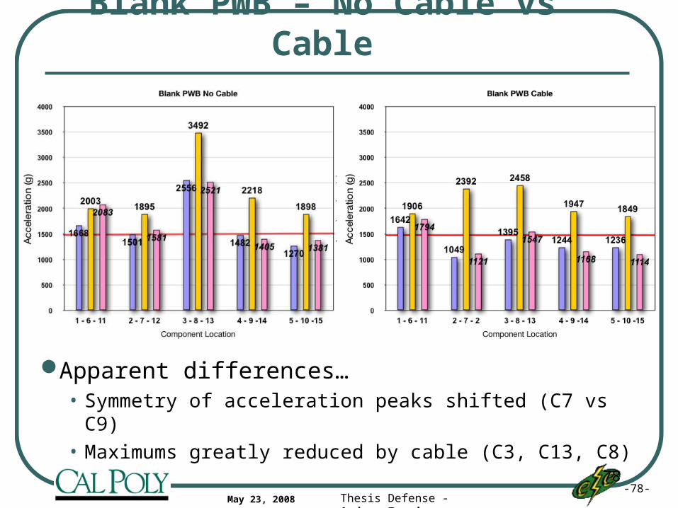
Blank PWB – No Cable vs Cable
Apparent differences…• Symmetry of acceleration peaks shifted (C7 vs C9)
• Maximums greatly reduced by cable (C3, C13, C8)78
-79-Thesis Defense - Andrew FarrisMay 23, 2008
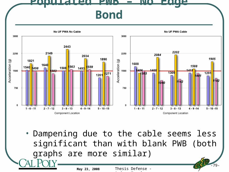
Populated PWB – No Edge Bond
• Dampening due to the cable seems less significant than with blank PWB (both graphs are more similar)
79
-80-Thesis Defense - Andrew FarrisMay 23, 2008
Epoxy Edge Bonded CSPs
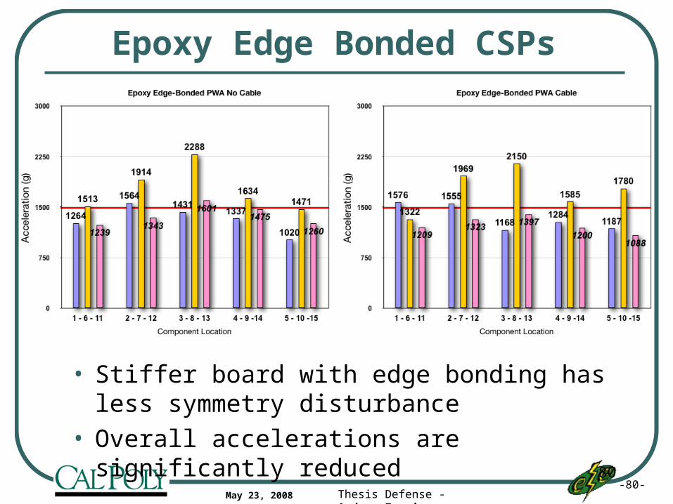
• Stiffer board with edge bonding has less symmetry disturbance
• Overall accelerations are significantly reduced80
-81-Thesis Defense - Andrew FarrisMay 23, 2008
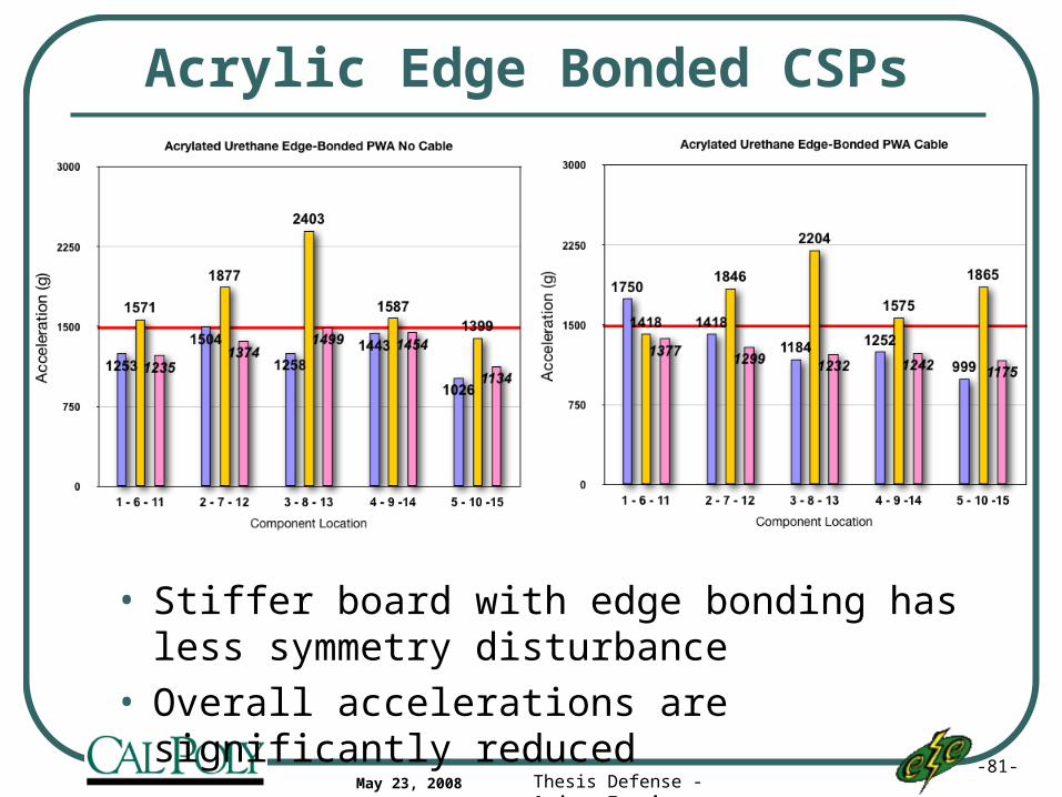
Acrylic Edge Bonded CSPs
• Stiffer board with edge bonding has less symmetry disturbance
• Overall accelerations are significantly reduced
-82-Thesis Defense - Andrew FarrisMay 23, 2008
Cable Influence on Acceleration
Symmetry of acceleration/deflection/strain is effected:• A cable soldered to the PWB will effect the test
conditions for any test vehicle assembly
• Components cannot be grouped as liberally for reliability statistics if test conditions at their locations are not similar
Lightest possible wire gauge should be used• But must provide reliable through-hole solder
joints
82
-83-Thesis Defense - Andrew FarrisMay 23, 2008
Cable Influence on Acceleration
Attaching a cable to both board ends could restore symmetry, but will also…• Add mass to the test vehicle
• Increase vibration dampening
• Decrease the effects of harmonic vibration frequencies
• Decrease total deflection (cantilever effect of the wire mass)
83
-84-Thesis Defense - Andrew FarrisMay 23, 2008
Agenda
Drop Impact TestingAnalysis
• Reliability Data
• Failure Mechanisms
• Acceleration on Test Vehicle
ConclusionsAcknowledgements
-85-Thesis Defense - Andrew FarrisMay 23, 2008
Conclusions
The component location on the test vehicle has a significant role in reliability• Components near the board center tend to fail first
Higher acceleration conditions decrease the drops to failure, resulting in lower reliability
Edge bonding significantly increases the reliability of lead-free CSPs in drop impact conditions
-86-Thesis Defense - Andrew FarrisMay 23, 2008
Conclusions
Cohesive failure between the resin and the board fiberglass leads to pad cratering
Pad cratering causes trace breakage and is the most common electrical failure mode
Board laminate materials for this lead-free test vehicle are the weakest link in the assembly, rather than the solder joints

-87-Thesis Defense - Andrew FarrisMay 23, 2008
Acknowledgements
Dr. John Pan (IME), Dr. Albert Liddicoat (EE), AdvisorsDr. James Harris (EE), Thesis committee memberProject Sponsors:
Office of Naval Research (ONR)
Through California Central Coast Research Park (C3RP)Society of Manufacturing Engineers Education FoundationSurface Mount Technology Association (SMTA)
87
-88-Thesis Defense - Andrew FarrisMay 23, 2008
Acknowledgements
Multidisciplinary team of students:• Nicholas Vickers (MATE), Kyle Rauen (MATE), and
Ronald Sloat (GE) assisted with failure analysis
• Michael Krist (IE) and Micah Denecour (IE) assisted with reliability data analysis
• Edward Clements (MFGE) and Chi-Yeh Hsu (ME) built and tested the first data acquisition system prototype
• Keith Rothman (AERO) wrote the first version of the DAQ system control software
88
-89-Thesis Defense - Andrew FarrisMay 23, 2008
Questions
How do you find an electrical engineer? Look for the ‘Desk’.http://comicstripjoint.blogspot.com

-90-Thesis Defense - Andrew FarrisMay 23, 2008
Supplemental Slides

-91-Thesis Defense - Andrew FarrisMay 23, 2008
SMT Assembly (stencil printing)
Stencil (DEK)• 4 mils thick
• Electro-Polish
• 12 mils square apertures
Stencil Printing• Front/Rear Speed: 40 mm/s
• Front/Rear Pressure: 12 kg
• Squeegee length: 300mm
• Separation Speed: 10 mm/s
-92-Thesis Defense - Andrew FarrisMay 23, 2008
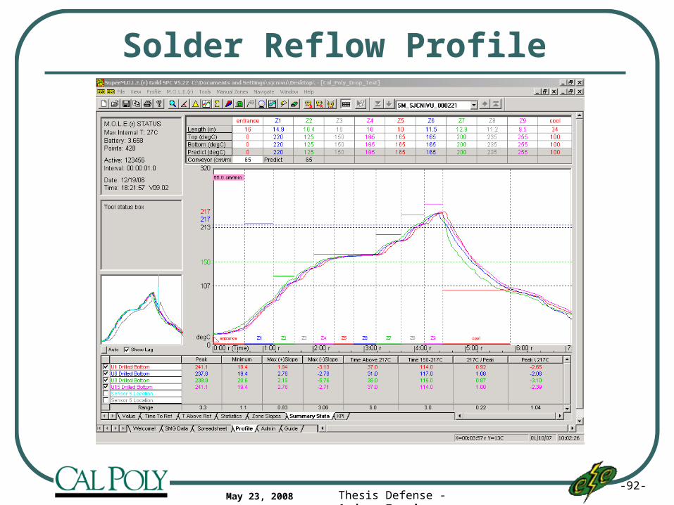
Solder Reflow Profile
-93-Thesis Defense - Andrew FarrisMay 23, 2008
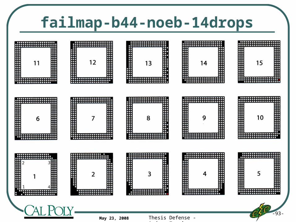
failmap-b44-noeb-14drops

-94-Thesis Defense - Andrew FarrisMay 23, 2008
failmap-b41-noeb-10drops
-95-Thesis Defense - Andrew FarrisMay 23, 2008
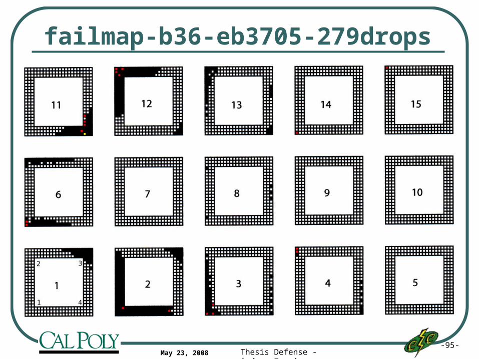
failmap-b36-eb3705-279drops
-96-Thesis Defense - Andrew FarrisMay 23, 2008
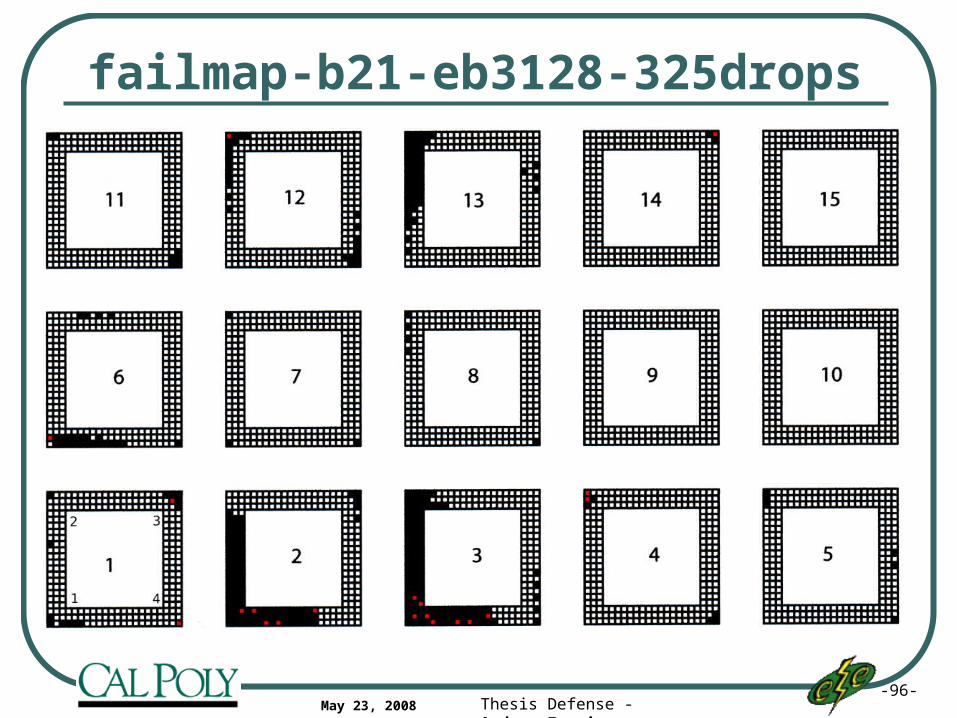
failmap-b21-eb3128-325drops